Graphene, Nobel Prize and All that Jazz 111To be published in Physics in Canada
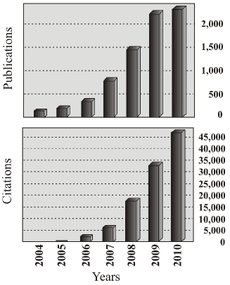
Graphene, a single atomic layer of graphite, first isolated in 2004 novo_science , has made a quantum leap in the exploration of the physics of two-dimensional electron systems review ; my_pic . Since the initial report of its discovery, many thousands of papers have been published (Fig. 1), attempting to explain every aspect of the exotic electronic properties of this system. The graphene euphoria has culminated with the 2010 Nobel Prize in physics being awarded jointly to Andre Geim and Konstantin Novoselov of the University of Manchester, UK, “for groundbreaking experiments regarding the two-dimensional material graphene”. But, what are the properties of graphene, and how was it made? Why it is so exciting for so many researchers, and why the Nobel Prize?
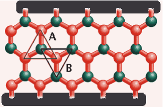
The saga of the exotic electronic properties of graphene actually began in Canada, when the band structure of graphene was first reported in a seminal paper by Philip R. Wallace (then at the National Research Council of Canada, Chalk River) wallace . Graphene is a single sheet of carbon atoms arranged in a honeycomb (hexagonal) lattice (a molecular chicken wire where one carbon atom sits at each 120∘ corner) (Fig. 2). This material is perhaps the ultimate two-dimensional system possible, with very unique electronic properties that are entirely different (and unexpected) from those of conventional two-dimensional systems ando . Graphene is a bipartite lattice made up of two interpenetrating triangular sublattices. There are two carbon atoms (commonly referred to as A and B) per unit cell. Each carbon atom has one orbital and two in-plane orbitals which make up the strong covalent bonds responsible for the mechanical stability of the graphene sheet. The remaining orbital, pointing out of the graphene sheet, form the conduction and valence bands with the neighboring orbitals.
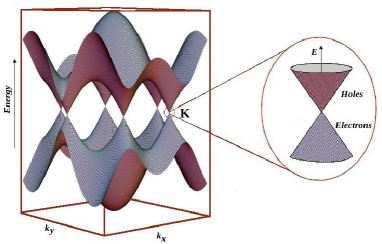
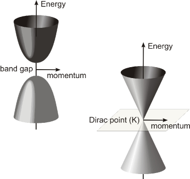
The dynamics of electrons in graphene can be described by a tight-binding Hamiltonian with nearest-neighbor hopping. Using this approach, Wallace derived the band structure of graphene as shown in Fig. 3. There are six points where the valence (upper) and conduction (lower) bands meet. Two of those points are inequivalent and are usually denoted by K and K′ review . In pristine graphene, the Fermi level lies right at the meeting points, rendering graphene a zero-band gap semiconductor. For reasons that will be clear below, these points are known as Dirac (or charge neutrality) points. Close to the Dirac points the charge carrier dispersion relation is, , where the momentum is measured with respect to the K (or K′) point. Here, , being the speed of light, is the Fermi velocity. Clearly, the charge carriers behave as if they were massless relativistic particles (obeying the Dirac equation rather than the Schrödinger equation), and display properties that are completely different from those in conventional metals or semiconductors, where the energy dispersion is parabolic (Fig. 4).
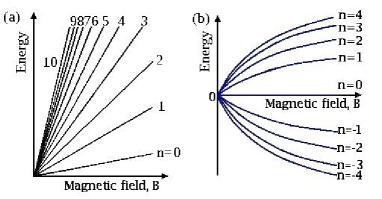
In the presence of an external magnetic field, the energies of electrons in conventional two-dimensional systems are quantized as Landau levels that are linearly proportional to the magnetic field (Fig. 5). In the quantum limit, i.e., at low temperatures when the thermal energy is much less than the level spacing, and at high magnetic fields when the Landau level spacings are large, the integer quantum Hall effect (QHE) was discovered in 1980 book (Nobel prize in 1985). In the extreme quantum limit, i.e., at very high fields and very low temperatures, and in samples with very high electron mobility, the fractional QHE was discovered in 1982 book (Nobel prize in 1998). How does the situation differ in the case of graphene? Back in 1956, McClure reported mcclure that the linear dispersion of energy dictates a very different type of Landau level: ones with square-root dependence on the magnetic field, and presence of a level at zero energy that is independent of the magnetic field (Fig. 5). In this case, an unusual QHE, the so-called half-integer QHE was expected sharapov . Experimental observation of this half-integer QHE novo_nature ; kim_nature firmly established the existence of massless Dirac type of behavior of charge carriers in graphene. This momentous observation sparked intense interest in the electronic properties of graphene that we are still witnessing today.
Graphite is composed of stacked layers of graphene with weak interlayer coupling by the van der Waals force. Isolated sheets of graphene which eluded us for many years, were actually prepared by a remarkably simple, and yet efficient method by Geim and Novoselov novo_science . The process is called mechanical exfoliation (a formal name for a pedestrian ‘scotch tape’ technique), where graphite flakes are produced by repeated peeling of graphite with adhesive tapes until some of the flakes are found to be monolayers (as determined by optical microscopy). The flakes are then deposited on a silicon wafer with an SiO2 top layer of thickness 300 nm. The one-atom-thick bits of graphene were found to remain surprisingly stable even at room temperature novo_science .
The Scotch-tape ”synthesis” method, prosaic in the face of epitaxial technology, isn’t likely to produce large quantities of graphene. In the race to achieve graphene in large quantities various other techniques have been reported in the literature synthesis . The goal to grow uniform, large piece of graphene that are suitable for graphene-based electronics, has achieved only a limited success.
Extensive research on graphene in the past five years have accumulated a wealth of information on the properties of graphene. It (a) shows ballistic transport over sub-micron scales with very high mobilities when suspended morozov ; communication , (b) can withstand large current densities novo_science , (c) is almost impermeable to gases bunch , (d) is chemically stable, and (e) has high thermal conductivity, among others. These appealing traits make graphene a very promising candidate for nano-electronics applications.
Can graphene replace silicon based transistors? The carrier mobilities in graphene are hundreds of times higher than in silicon chips used today. However, there is a ‘slight’ problem with graphene, it has no band gap! A gap between the conduction and valence band allows semiconductors to be easily turned on and off. On the other hand, the absence of a band gap allows absorption of light in a large range of the electromagnetic spectrum. Therefore it opens a huge potential for applications of graphene in electronic-photonic devices. The problems related to the absence of a band gap in graphene, in its use in field-effect transistors, can be circumvented by using graphene nanoribbons instead han ; avouris . A thin film of graphene has very high transparency and combined with high electrical conductivity makes graphene an ideal candidate for transparent conductive coatings. This has already been demonstrated in graphene based solar cells solar . Graphene membranes, just one-atom thick were shown to stretch like a balloon, yet strong enough to contain gases under several atmosphere of pressure without bursting bunch . Chemical modification of graphene is a promising route to create a band gap. Adsorption of hydrogen on a graphene surface creates a new system, named graphane graphane . The electronic properties of the new material change markedly by having a band gap. The new system might be the testing ground for unique magnetic properties julia suitable for spin based electronics.
Quantum dots (QDs), or artificial atoms QD_book are one of the most intensely studied systems in condensed matter physics, where the fundamental effects related to various quantum phenomena in confined geometries can be studied but with the unique advantage that the nature of the confinement and the electron density can be tuned externally. However, much of the interest in this system derives from its enormous potential for applications, ranging from novel lasers to quantum information processing. While the majority of the QD systems investigated are based on the semiconductor heterostructures, research on QDs created from graphene have been reported review ; QD_graphene ; qdots_expt recently.
By stacking one more layer on graphene, one gets bilayer graphene, which is a fascinating and complex system in its own right, distinct from both the monolayer and traditional two-dimensional electron systems, even though it shares some characteristics of each review . It has a quadratic low-energy band structure and the charge carriers are massive, unlike the massless nature in the case of monolayers bilayer . One notable feature of bilayer graphene is the ability to open a tunable band gap by engineering a potential difference between the two layers, suitable for the construction of devices. Understanding the role electron-electron interactions play in bilayer graphene might be the key to explain many of the important features observed in this system david .
As stated above, the observation of a half-integer QHE in graphene opened the floodgate of enthusiasm for graphene-related research. Interestingly, the “other” QHE, the fractionally quantized Hall effect was explored by this author theoretically for monolayer vadim_fqhe and bilayer vadim_bilayer graphene. The effect has been recently observed experimentally in monolayer graphene fqhe_kim . This is an important milestone in graphene research, in particular, for investigation of highly correlated electrons in graphene.
The award of this year’s Nobel prize is a strong testament to the fact that in these days when ground breaking discoveries in science are thought to come exclusively from multi-billion dollar particle accelerators searching for the elusive bosons, or telescopes in space zooming in on truly unreachable exoplanets, fundamental and profound discoveries can also be made with a tiny piece of graphite and ordinary sticky tape. Interestingly, this award has also been given for a reason that is totally opposite to not-so-unrelated discoveries of the integer and fractional quantum Hall effects. Those discoveries were recognized by the awards which somewhat overshadowed the extraordinary developments in materials where those effects were discovered and how those materials advanced the semiconductor technology. In graphene, on the other hand, thanks to pioneers such as Wallace and McClure, there were plenty of valuable insights already available. The challenge was to create materials where those predictions could be verified. Geim and Novoselov were successful in doing just that. Award of this Nobel Prize highlights the importance of graphene in nanotechnology. We will have to wait and see if graphene the ‘wunder material’ would actually face up to the mighty challenger, silicon, and surpass its prowess in future nanoscale electronic devices.
My research work cited in this article was supported by the Canada Research Chairs Program. I wish to thank Dr. Julia Berashevich for her help in preparing this article. I also thank Vadim Apalkov for a critical reading of the article.
References
- (1) Electronic address: tapash@physics.umanitoba.ca
- (2) K.S. Novoselov, A.K. Geim, S.V. Morozov, D. Jiang, Y. Zhang, S.V. Dubonos, I.V. Grigorieva and A.A. Firsov, “Electric field effect in atomically thin carbon films”, Science 306, 666-669 (2004).
- (3) For a current review on graphene, see, D.S.L. Abergel, V. Apalkov, J. Berashevich, K. Ziegler, and T. Chakraborty, “Properties of graphene: a theoretical perspective”, Adv. Phys. 59, 261-482 (2010).
- (4) T. Chakraborty, “Graphene: A nanoscale quantum playing field”, Physics in Canada 62, 351-354 (2006).
- (5) P.R. Wallace, “The band theory of graphite”, Phys. Rev. 71, 622-634 (1947).
- (6) T. Ando, A.B. fowler, and F. Stern, “Electronic properties of two-dimensional systems”, Rev. Mod. Phys. 54, 437-672 (1982).
- (7) J.W. McClure, “Diamagnetism of graphite”, Phys. Rev. 104, 666-671 (1956). See also, R.R. Haering and P.R. Wallace, “The electric and magnetic properties of graphite”, J. Phys. Chem. Solids 3, 253-274 (1957).
- (8) T. Chakraborty, and P. Pietiläinen, The Quantum Hall Effects (Springer, New York, 1995), 2nd edition.
- (9) V.P. Gusynin and S.G. Sharapov, “Unconventional integer quantum Hall effect in graphene”, Phys. Rev. Lett. 95, 146801 (2005).
- (10) K.S. Novoselov, A.K. Geim, S.V. Morozov, D. Jiang, M.I. Katsnelson, I.V. Grigorieva, S.V. Dubonos and A.A. Firsov, “ Two-dimensional gas of massless Dirac fermions in graphene”, Nature 438, 197-200 (2005).
- (11) Y. Zhang, Y.-W. Tan, H.L. Stormer and P. Kim, “Experimental observation of the quantum Hall effect and Berry’s phase in graphene”, Nature 438, 201-204 (2005).
- (12) Wonbong Choi, et al., “Synthesis of graphene and its applications: A review”, Critical Reviews in Solid State and Materials Sciences 35 52-71 (2010).
- (13) S.V. Morozov, et al., “Giant intrinsic carrier mobilities in graphene and its bilayer”, Phys. Rev. Lett. 100, 016602 (2008).
- (14) K.I. Bolotin, et al., “Ultrahigh electron mobility in suspended graphene”, Solid State Commun. 146, 351-355 (2008).
- (15) J. Scott Bunch, et al., “Impermeable atomic membranes from graphene sheets”, Nano Lett. 8, 2458-2462 (2008).
- (16) X. Wang, L. Zhi, K. Müllen, “Transparent, conductive graphene electrodes for dye-sensitized solar cells”, Nano Lett. 8, 323-327 (2008).
- (17) M.Y. Han, B. Özyilmaz, Y. Zhang, and P. Kim, “Energy band-gap engineering of graphene nanoribbons”, Phys. Rev. Lett. 98, 206805 (2007).
- (18) Z. Chen, Y.-M. Lin, M.J. Rooks, and P. Avouris, “Graphene nano-ribbon electronic”, Physica E 40, 228-232 (2007).
- (19) M.Z.S. Flores, et al., “Graphene to graphane: a theoretical study”, Nanotechnology 20, 465704 (2009).
- (20) J. Berashevich and T. Chakraborty, “Sustained ferromagnetism induced by H-vacancies in graphane”, Nanotechnology 21, 355201 (2010).
- (21) T. Chakraborty, Quantum Dots (Elsevier, 1999).
- (22) H.-Y. Chen, V. Apalkov, and T. Chakraborty, “Fock-Darwin states of Dirac electrons in graphene-based artificial atoms”, Phys. Rev. Lett. 98, 186803 (2007).
- (23) T. Ihn, et al., “Graphene single-electron transistors”, Materials Today 13, 44-50 (2010).
- (24) E. McCann and V.I. Falko, “Landau-Level Degeneracy and quantum Hall effect in a graphite bilayer”, Phys. Rev. Lett. 96, 086805 (2006).
- (25) D.S.L. Abergel and T. Chakraborty, “Long-range Coulomb interaction in bilayer graphene”, Phys. Rev. Lett. 102, 056807 (2009); X. F. Wang and T. Chakraborty, “Coulomb screening and collective excitations in a graphene bilayer”, Phys. Rev. B 75, 041404(R) (2007).
- (26) V.M. Apalkov and T. Chakraborty, “Fractional quantum Hall states of Dirac electrons in graphene”, Phys. Rev. Lett. 97, 126801 (2006).
- (27) V. Apalkov and T. Chakraborty, “Controllable driven phase transitions in fractional quantum Hall state in bilayer graphene”, Phys. Rev. Lett. 105, 036801 (2010).
- (28) K.I. Bolotin, F. Ghahari, M.D. Shulman, H.L. Störmer, and P. Kim, “Observation of the fractional quantum Hall effect in graphene”, Nature 462, 196-199 (2009); see also, X. Du, et al., “Fractional quantum Hall effect and insulating phase of Dirac electrons in graphene”, Nature 462, 192-195 (2009).