Unity absorbance layers - optimal design criteria
Abstract
We present the necessary and sufficient conditions for the unity absorbance of thin planar layers. With a simple structure comprising a double-layer grid, it is shown that zero transmission and reflection is feasible only if the second sheet is a perfectly conducting wall. The operational frequencies can be varied by tuning the grid impedance. Explicit conditions are given at the large wavelength limit; these underline the fundamental of ultra-thin perfect antennae and absorbers.
-
1Low Temperature Laboratory, Aalto University, P.O. Box 15100, FI-00076 Aalto, Finland
2Department of Radio Science and Engineering, Aalto University, P.O. Box 13000, FI-00076, Aalto, Finland
1. Introduction
In this paper we will discuss the possibility to design and realize planar layers that absorb all incident power of plane waves at normal incidence (zero reflection, zero transmission, unity absorbance). It is obvious that if the layer is an infinitely thin sheet of induced electric current, this is not possible to realize. This is because a sheet of electric current radiates symmetrically in the forward and back direction, so the requirement of zero reflection means the absence of shadow (unity transmission). Thus, if no magnetic materials are to be used, the unity-absorbance layer must have non-zero thickness. If the back surface is an impenetrable wall, for example a perfect electric conductor (PEC) surface, the design of unity absorbance layers is trivial, [1], for example, by positioning a resistive sheet at the quarter-wave distance from the PEC plane and choose its electrical surface admittance to be equal to that of free space. The sheet can be brought closer to the wall by adding appropriate reactance in the sheet response (such absorbers are well known). We are, however, interested in the case when no impenetrable wall is present. This way one can realize layers that are transparent in some frequency ranges but absorb all power at some other frequencies. Recently, some numerical and experimental results for such absorbing layers were published, but the design was based on numerical simulations, and no ideal performance (zero transmission and zero reflection at the same frequency) has been demonstrated. Here, we will theoretically consider a possible realization using two parallel infinitely thin sheet separated by a free-space layer.
2. Matched unity absorbance layers criteria
Natural materials are known to exhibit high absorption at some frequencies. But tailoring a natural material to achieve perfect absorption over a frequency bandwidth is not straightforward. Within the last two years, there has been many attempts to realize devices with near unity absorbance [2]-[8].
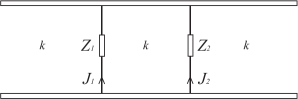
In this paper, we discuss and analyze the optimal criteria to realize perfect absorption at normal incidence. The theory is drawn based on the transmission-line model of a double-layer planar grids, Fig. 1. The structure is specified with grid impedances and average surface current densities .
By applying the the grid condition, , [9], we obtain, at the first load,
| (1) |
and at the second load,
| (2) |
Solving Eq. (1) and (2), we determine the average current densities. The reflected field and transmitted fields are related to the current densities on the grids as
| (3) |
| (4) |
By definition, and , and we can express the reflection and transmission coefficients in terms of the grid parameters:
| (5) |
| (6) |
The trivial solutions for zero transmission are the cases in which one of the grid impedances is zero, a short-circuit. To obtain non-trivial solutions for total absorption, we firstly set the reflection coefficient in Eq. (5) to zero to obtain the optimal condition for the grid impedances
| (7) |
Substituting this back to Eq. (6) reveals the relation between the transmission coefficient and :
| (8) |
Eqs. (7) and (8) constitute the conditions for unity absorbance in terms of the grid parameters and electrical thickness of the spacing: , and . Note that is the wave vector of the medium filling the space between the two grids, which is assumed to the same as the surrounding medium.
3. Discussion and conclusion
The results show that it is actually not possible to realize perfect absorbers (such that at some frequency both ) except if the second sheet is a perfectly conducting layer. The well-known absorber design based on a lossy and possibly reactive thin sheet parallel to a PEC wall is seen to be the only solution. For thin layers, using the Taylor expansion of Eq. (9), the required grid impedance of the first sheet reads
| (10) |
If only passive materials are used in the design, the ideal operation is possible only at a single frequency. This is obvious since the required reactance of the first grid corresponds to a lossless negative inductance and the frequency-decreasing reactance of a lossless structure is incompatible with the causality principle of material response (the Kramers-Kronig relations and the Foster theorem are violated). Wide bandwidth in this design is possible only if active or tunable components are used. Another classical design follows, from Eq. (9), when the first grid is a quarter wavelength away from the PEC wall (), in this case the required is purely resistive with .
In the future, we plan to study possibilities offered by more general configurations, with material layers between the grids or more than two grids, and find out if unit-absorbance layers can be designed without utilizing perfect electric conductors.
Acknowledgements
This topic was first proposed by ST as a subject of a student research project within the post-graduate course “Analytical modeling in applied electromagnetics” (Helsinki University of Technology, 2009). The work is financially supported by Thailand Commission on Higher Education and the Academy of Finland.
References
- [1] R. L. Fante and M. T. McCormack, Reflection properties of the salisbury screen, IEEE. Trans. Antennas Propagat., vol. 36, p. 1443-1454, 1988.
- [2] V. G. Kravets, F. Schedin, and A. N. Grigorenko, Plasmonic blackbody: Almost complete absorption of light in nanostructured metallic coatings, Phys. Rev. B., vol. 78, p. 205405, 2008.
- [3] N. I. Landy, S. Sajuyigbe, J. J. Mock, D. R. Smith, andW. J. Padilla, Perfect metamaterial absorber, Phys. Rev. Lett., vol. 100, p. 207402, 2008.
- [4] H. Tao, N. I. Landy, C. M. Bingham, X. Zhang, R. D. Averitt, and W. J. Padilla, A metamaterial absorber for the terahertz regime: design, fabrication and characterization, Optics Express, vol. 16, p. 7181, 2008.
- [5] Zhu Bo, Wang Zheng-Bin, Yu Zhen-Zhong, Zhang Qi, Zhao Jun-Ming, Feng Yi-Jun, Jiang Tian, Planar metamaterial microwave absorber for all wave polarizations, Chin. Phys. Lett., vol. 26, 114102, 2009.
- [6] M. Diem, T. Koschny, and C. M. Soukoulis, Wide-angle perfect absorber/thermal emitter in the terahertz regime, Phys. Rev. B, vol. 79, 033101, 2009.
- [7] E. F. C. Driessen and M. J. A. de Dood, The perfect absorber, Appl. Phys. Lett., vol. 94, 171109, 2009.
- [8] J. F. Wang, S. B. Qu, Z. T. Fu, H. Ma, Y. M. Yang and X. Wu, Three-dimensional metamaterial microwave absorbers composed of coplanar magnetic and electric resonators, Progress in Electromagnetics Research Letters, vol. 7, p. 15-24, 2009.
- [9] S. Tretyakov, Analytical Modeling in Applied Electromagnetics, Artech House, 2003.