Mesoscopic Physics and Nanoelectronics
Abstract
Electronic transport properties through some model quantum systems are re-visited. A simple tight-binding framework is given to describe the systems where all numerical calculations are made using the Green’s function formalism. First, we demonstrate electronic transport in four different polycyclic hydrocarbon molecules, namely, benzene, napthalene, anthracene and tetracene. It is observed that electron conduction through these molecular wires is highly sensitive to molecule-to-electrode coupling strength and quantum interference of electronic waves passing through different branches of the molecular ring. Our investigations predict that to design a molecular electronic device, in addition to the molecule itself, both the molecular coupling and molecule-to-electrode interface geometry are highly important. Next, we make an in-depth study to design classical logic gates with the help of simple mesoscopic rings, based on the concept of Aharonov-Bohm effect. A single mesoscopic ring or two such rings are used to establish the logical operations where the key controlling parameter is the magnetic flux threaded by the ring. The analysis might be helpful in fabricating meso-scale or nano-scale logic gates. Finally, we address multi-terminal quantum transport through a single benzene molecule using Landauer-Büttiker formalism. Quite interestingly we see that a three-terminal benzene molecule can be operated as an electronic transistor and this phenomenon is justified through current-voltage characteristics. All these essential features of electron transport may provide a basic theoretical framework to examine electron conduction through any multi-terminal quantum system.
pacs:
73.23.-b, 73.63.Rt, 73.40.Jn, 73.63.-b, 81.07.Nb, 85.65.+hI Introduction
I.1 Basic concepts
Mesoscopic physics is a sub-discipline of condensed matter physics which deals with systems whose dimensions are intermediate between the microscopic and macroscopic length scales imrybook ; datta1 ; datta2 ; metalidis ; weinmann . In meso-scale region fluctuations play an important role and the systems are treated quantum mechanically, in contrast to the macroscopic objects where usually the laws of classical mechanics are used. In a simple version we can say that a macroscopic system when scaled down to a meso-scale starts exhibiting quantum mechanical phenomena. The most relevant length scale of quantifying a mesoscopic system is probably the phase coherence length , the length scale over which the carriers preserve their phase information. This phase coherence length is, on the other hand, highly sensitive to temperature and sharply decreases with the rise of temperature. Therefore, to be in the mesoscopic regime we have to lower the temperature sufficiently (of the order of liquid He) such that phase randomization process caused by phonons gets minimum. Though there is no such proper definition of the mesoscopic region, but the studied mesoscopic objects are normally in the range of - nanometers.
Several spectacular effects appear as a consequence of quantum phase coherence of the electronic wave functions in mesoscopic systems like one-dimensional (D) quantum wires, quantum dots where electrons are fully confined, two-dimensional (D) electron gases in heterostructures, etc. For our illustrative purposes here we describe very briefly some of these issues.
(i) Aharonov-Bohm Effect: One of the most significant experiments in mesoscopic physics is the observation of Aharonov-Bohm (AB) oscillations in conductance of a small metallic ring threaded by a magnetic flux webb1 ; webb2 . The origin of conductance oscillations lies in the quantum interference among the waves traversing through two arms of the ring. This pioneering experiment has opened up a wide range of challenging and new physical concepts in the mesoscopic regime.
(ii) Conductance Fluctuations: The pronounced fluctuations in conductance of a disordered system are observed when the temperature is lowered below K webb3 . These fluctuations are originated from the interference effects of the electronic wave functions traveling across the system and are fully different from the fluctuations observed in traditional macroscopically large objects. The notable feature of conductance fluctuations in the mesoscopic regime is that their magnitudes are always of the order of the conductance quantum , and accordingly, these fluctuations are treated as ‘universal conductance fluctuations’ fuku .
(iii) Persistent Current: In thermodynamic equilibrium a small metallic ring threaded by magnetic flux supports a current that does not decay dissipatively even at non-zero temperature. It is the well-known phenomenon of persistent current in mesoscopic normal metal rings butt ; levy ; mailly1 ; chand ; jari ; deb ; butt1 ; cheu1 ; cheu2 ; blu ; san1 ; san2 ; san3 ; san4 ; san5 . This is a purely quantum mechanical effect and gives an obvious demonstration of the AB effect aharo .
(iv) Integer Quantum Hall Effect: The integer quantum Hall effect is probably the best example of quantum phase coherence of electronic wave functions in two-dimensional electron gas (2DEG) systems klit . In the Hall experiment, a current is allowed to pass through a conductor (2DEG), and, the longitudinal voltage and transverse Hall voltage are measured as a function of the applied magnetic field which is perpendicular to the plane of the conductor. In the limit of weak magnetic field, the Hall resistance varies linearly with the field strength , while the longitudinal resistance remains unaffected by this field. These features can be explained by the classical Drude model. On the other hand for strong magnetic field and in the limit of low temperature a completely different behavior is observed and the classical Drude model fails to explain the results. In high magnetic field shows oscillatory nature, while shows step-like behavior with sharp plateaus. On these plateaus the values of are given by , being an integer, and they are highly reproducible with great precision. These values are extremely robust so that they are often used as the standard of resistance. The integer quantum Hall effect is a purely quantum mechanical phenomenon due to the formation of the Landau levels and many good reviews on IQHE are available in the literature imrybook ; pran ; chakra .
(v) Fractional Quantum Hall Effect: Unlike the integer quantum Hall effect, at too high magnetic fields and low temperatures, a two-dimensional electron gas shows additional plateaus in the Hall resistance at fractional filling factors tsui . It has been verified that the Coulomb correlation between the electrons becomes important for the interpretation of the fractional quantum Hall effect and the presence of fractional filling has been traced back to the existence of correlated collective quasi-particle excitations laug . Extensive reviews on this topic can be found in the literature chakra .
In the mesoscopic regime, electronic transport cannot be investigated by using the conventional Boltzmann transport equation since at this length scale quantum phase coherence plays an important role and a full quantum mechanical treatment is needed datta1 ; datta2 . In an ‘open system’ the Landauer approach land of ‘two-terminal conductance’ provides an elegant technique to reveal the transport mechanisms. In the Landauer formalism a quantum system is sandwiched between two macroscopic reservoirs, the so-called electrodes, those are kept at thermal equilibrium. By applying a bias voltage we tune the chemical potentials of these electrodes. The main signature of the electrodes is that electrons passing through them along the longitudinal direction can be described as plane waves and suffer no backscattering whatsoever. This allows us to describe the properties of the conductor in terms of its scattering matrix on the basis of plane waves within the electrodes. The Landauer formulation is probably the simplest and elegant approach for studying electron transport in low-dimensional quantum systems.
Ongoing trend of miniaturizing electronic devices eventually approaches the ultimate limit where even a single molecule can be used as an electrical circuit element. Idea of devicing a single molecule as the building block of future generation electronics seems fascinating because of the possibility to assemble a large number of molecules onto a chip i.e., remarkable enhancement in integration density can take place ratner1 . Discovery of sophisticated molecular scale measurement methodologies such as scanning tunneling microscopy (STM), atomic force microscopy (AFM), scanning electro-chemical microscopy (SECM), etc., have made it possible to study electron transport phenomena in molecular bridge systems chen .
The idea of using molecules as active components of a device was suggested by Aviram and Ratner aviram over three decades ago. Since then several ab-initio and model calculations have been performed to investigate molecular transport theoretically ventra1 ; ventra2 ; sumit ; tagami ; orella1 ; orella2 ; arai ; baer1 ; baer2 ; baer3 ; walc1 ; walc2 ; tagami1 ; tagami2 ; san6 ; san7 ; san8 ; san9 ; san10 ; san11 ; noza ; maas . But experimental realizations took a little longer time to get feasible. In , Reed and co-workers reed1 have studied the current-voltage (-) characteristics of a single benzene molecule attached to electrodes via thiol groups. Later various other experiments have been made to explore many interesting features e.g., ballistic transport, quantized conductance, negative differential resistance (NDR) saiful , molecular transistor operation park ; tao to name a few.
In short we can say that the rapid progress of theoretical as well as experimental works on mesoscopic physics over the last few decades proves that it is a highly exciting and challenging branch of condensed matter physics and we hope that it will be continuing for many more decades.
I.2 Aim of the review
In this dissertation we address several important issues on electron transport through some meso-scale systems which are quite challenging from the standpoint of theoretical as well as experimental research. A brief outline of the presentation is as follow.
On the meso-scale organic molecules, cluster of atoms, quantum dots, carbon nanotubes, etc., can be produced with flexible and tunable conduction properties and these new realities have tremendous technological importance. The physics of electron transport through such devices is surprisingly rich. Many fundamental experimentally observed phenomena in such devices can be understood by using simple arguments. In particular, the formal relation between conductance and transmission coefficients (the Landauer formula) has enhanced the understanding of electronic transport in the molecular bridge system. To reveal these facts, in the first part of this review we investigate electron transport properties of some molecular bridge systems within the tight-binding framework using Green’s function technique and try to explain the behavior of electron conduction in the aspects of quantum interference of electronic wave functions, molecule-to-electrode coupling strength, molecular length, etc. Our model calculations provide a physical insight to the behavior of electron conduction through molecular bridge systems.
Next, we explore the possibilities of designing classical logic gates at meso-scale level using simple mesoscopic rings. A single ring is used for designing OR, NOT, XOR, XNOR and NAND gates, while AND and NOR gate responses are achieved using two such rings and in all these cases each ring is threaded by a magnetic flux which plays the central role in the logic gate operation. We adopt a simple tight-binding Hamiltonian to describe the model where a mesoscopic ring is attached to two semi-infinite one-dimensional non-magnetic electrodes. Based on single particle Green’s function formalism all calculations which describe two-terminal conductance and current through the quantum ring are performed numerically. The analysis may be helpful in fabricating mesoscopic or nano-scale logic gates.
Finally, in the last part, we focus our attention on the multi-terminal transport problem. Here we no longer use the Landauer approach. Büttiker has extended the study of two-terminal quantum transport into the multi-terminal case which is known as Landauer-Büttiker formalism. With this approach we study multi-terminal quantum transport in a single benzene molecule to examine the transport properties in terms of conductance, reflection probability and current-voltage characteristics.
II Two-terminal molecular transport
Molecular electronics is an essential technological concept of fast-growing interest since molecules constitute promising building blocks for future generation of electronic devices where electronic transport becomes coherent ratner1 ; nitzan1 . For purposeful design of an electronic circuit using a single molecule or a cluster of molecules, the most important requirement is the understanding of fundamental processes of electron conduction through separate molecules used in the circuit. A fruitful discussion of electron transport in a molecular wire was first studied theoretically by Aviram and Ratner during 1974 aviram . Later, numerous experiments have been made in different molecules placed between electrodes with few nano-meter separation reed1 ; saiful ; park ; tao ; metz ; fish ; reed2 ; tali ; sch ; mir1 ; mir2 ; maji ; weiss . It is very crucial to control electron transmission through such molecular electronic devices, and, though extensive studies have been done, yet the present understanding about it is not fully explored. For example, it is not very clear how molecular conduction is affected by geometry of the molecule itself or by the nature of its coupling to side attached electrodes. To construct an electronic device made with molecules and to utilize it properly we need a deep analysis of structure-conductance relationship. In a recent work Ernzerhof et al. ern1 have illustrated a general design principle based on several model calculations to reveal this concept. In presence of applied bias voltage a current passes through the molecule-electrode junction and it becomes a non-linear function of the applied voltage. The detailed description of it is quite complicated. Electron transport properties in molecular systems are highly sensitive on several quantum effects like quantum interference of electronic waves passing through different arms of the molecular rings, quantization of energy levels, etc. baer1 ; baer2 ; baer3 ; walc1 ; walc2 . The main motivation of studying molecular transport is that molecules are currently the subject of substantial theoretical, experimental and technological interest. Using molecules we can design logic gates, molecular switches, several transport elements that need to be well characterized and explained.
In this section we address the behavior of electron transport through some polycyclic hydrocarbon molecules based on a simple tight-binding framework. Though several ab initio yal ; ven ; xue ; tay ; der ; dam ; ern3 ; zhu1 ; zhu2 methods are used to enumerate electron transport in molecular systems, but simple parametric approaches are rather much helpful to understand the basic mechanisms of electron transport in detail. Beside this here we also make our attention only on the qualitative effects instead of the quantitative results which also motivate us to perform model calculations in the transport problem.
To describe the behavior of molecular transport let us first construct the methodology for two-terminal quantum transport through a simple finite sized conductor.
II.1 Theoretical Formulation
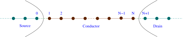
We begin with Fig. 1. A finite sized D conductor with atomic sites is attached to two semi-infinite D metallic electrodes, viz, source and drain. At much low temperature and bias voltage,
conductance of the conductor can be written by using Landauer conductance formula,
| (1) |
where, is the transmission probability of an electron through the conductor. In terms of the Green’s function of the conductor and its coupling to the side attached electrodes, transmission probability can be expressed as,
| (2) |
where, and are the retarded and advanced Green’s functions of the conductor, respectively. and are the coupling matrices due to the coupling of the conductor to the source and drain, respectively. For the combined system i.e., the conductor and two electrodes, the Green’s function becomes,
| (3) |
is the injecting energy of the source electron and is the Hamiltonian of the combined system. Evaluation of this Green’s function requires the inversion of an infinite matrix as the system consists of the finite size conductor and two semi-infinite D electrodes, which is really a very difficult task. However, the entire system can be partitioned into sub-matrices corresponding to the individual sub-systems, and then the Green’s function for the conductor can be effectively written as,
| (4) |
where, is the Hamiltonian of the conductor. Withing a non-interacting picture, the tight-binding Hamiltonian of the conductor looks like,
| (5) |
() is the creation (annihilation) operator of an electron at site , is the site energy of an electron at the -th site and corresponds to the nearest-neighbor hopping integral. A similar kind of tight-binding Hamiltonian is also used for the description of electrodes where the Hamiltonian is parametrized by constant on-site potential and nearest-neighbor hopping integral . In Eq. 4, and are the self-energy operators due to the two electrodes, where and are the Green’s functions for the source and drain, respectively. and are the coupling matrices and they will be non-zero only for the adjacent points in the conductor, and as shown in Fig. 1, and the electrodes respectively. The coupling terms and of the conductor can be calculated from the following expression,
| (6) |
Here, and are the retarded and advanced self-energies, respectively, and they are conjugate to each other. Datta et al. tian have shown that the self-energies can be expressed like,
| (7) |
where, are the real parts of the self-energies which correspond to the shift of the energy eigenvalues of the conductor and the imaginary parts of the self-energies represent the broadening of the energy levels. Since this broadening is much larger than the thermal broadening we restrict our all calculations only at absolute zero temperature. The real and imaginary parts of the self-energies can be determined in terms of the hopping integral () between the boundary sites ( and ) of the conductor and electrodes, energy () of the transmitting electron and hopping strength () between nearest-neighbor sites of the electrodes.
The coupling terms and can be written in terms of the retarded self-energy as,
| (8) |
Now all the information regarding the conductor to electrode coupling are included into these two self energies as stated above. Thus, by calculating the self-energies, the coupling terms and can be easily obtained and then the transmission probability () will be calculated from the expression as presented in Eq. 2.
Since the coupling matrices and are non-zero only for the adjacent points in the conductor, and as shown in Fig. 1, the transmission probability becomes,
| (9) |
where, , and .
The current passing through the conductor is treated as a single-electron scattering process between the two reservoirs of charge carriers. We establish the current-voltage relation from the expression datta1 ; datta2 ,
| (10) |
where, is the equilibrium Fermi energy. For the sake of simplicity, here we assume that the entire voltage is dropped across the conductor-electrode interfaces and it doesn’t greatly affect the qualitative aspects of the current-voltage characteristics. This is due to the fact that the electric field inside the conductor, especially for shorter conductors, seems to have a minimal effect on the conductance-voltage characteristics. On the other hand, for quite larger conductors and higher bias voltages, the electric field inside the conductor may play a more significant role depending on the internal structure of the conductor tian , though the effect becomes too small. Using the expression of (Eq. 9), the final form of is,
| (11) |
Eqs. 1, 9 and 11 are the final working expressions for the determination of conductance , transmission probability , and current , respectively, through any finite sized conductor placed between two D metallic reservoirs. Throughout our presentation, we use the units where , and, the energy scale is measured in unit of .
II.2 Molecular System and Transport Properties
Based on the above two-terminal transport formulation, in this section, we describe the behavior of electron conduction through some polycyclic hydrocarbon molecules those are schematically shown in Fig. 2. The molecules are: benzene (one ring), napthalene (two rings), anthracene (three rings) and tetracene (four rings). These molecules are connected to the electrodes (source and drain) via thiol (S-H bond) groups. In real experimental situations, gold (Au) electrodes are generally used and the molecules are coupled to them through thiol groups in the chemisorption technique where hydrogen (H) atoms removes ans sulfur (S) atoms reside. To emphasize the effect of quantum interference on electron transport, we couple the molecules to the source and drain in two different configurations. One is defined as cis configuration where two electrodes are placed at the sites, whereas in the other arrangement, called as trans configuration, electrodes are connected at the sites. Molecular coupling is another important factor which controls the electron transport. To justify this fact, here we describe the essential features of electron transport for the two limiting cases of molecular coupling. One is the weak-coupling limit which mathematically treated as and in the other case we have which is defined as the strong-coupling limit. and are the hopping strengths of the molecule to the source and

drain, respectively. The common set of values of the parameters used in the calculation are as follows. , (weak-coupling) and , (strong-coupling). In the electrodes we set and . The Fermi energy is fixed at .
II.2.1 Conductance-energy characteristics
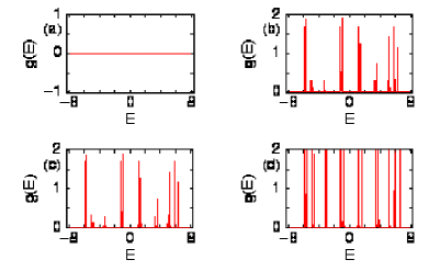
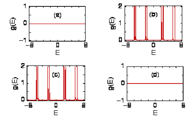
In Fig. 3, we show the behavior of conductance () as a function of injecting electron energy () for the hydrocarbon molecules when they are coupled to the electrodes in the trans configuration, where (a), (b), (c) and (d) correspond to the benzene, napthalene, anthracene and tetracene molecules, respectively. In the limit of weak molecular coupling, conductance shows sharp resonant peaks (solid lines) for some specific energy eigenvalues, while it drops almost to zero for all other energies. At the resonance, conductance approaches to , and therefore, the transmission probability () becomes unity (from the Landauer conductance formula in our chosen unit system ). The resonant peaks in the conductance spectrum coincide with eigenenergies of the single hydrocarbon molecules. Thus, from the conductance spectrum we can easily implement the electronic structure of a molecule. The nature of these resonant peaks gets significantly modified when molecular coupling is increased. In the strong-coupling limit, width of the resonant peaks gets broadened as shown by the dotted curves in Fig. 3 and it emphasizes that electron conduction takes place almost for all energy values. This is due to the broadening of the molecular energy levels, where contribution comes from the imaginary parts of the self-energies tian .
To establish the effect of quantum interference on electron transport, in Fig. 4, we plot conductance-energy characteristics for these molecules when they are connected to the electrodes in the cis

configuration. (a), (b), (c) and (d) correspond to the results for the benzene, napthalene, anthracene and tetracene molecules, respectively, where the solid and dotted curves indicate the identical meaning as in Fig. 3. From these spectra we clearly see that some of the conductance peaks do not reach to unity anymore and achieve much reduced amplitude. This behavior can be justified as follow. During the propagation of electrons from the source to drain, electronic waves which pass through different arms of the molecular ring/rings can suffer a phase shift among themselves, according to the result of quantum interference. As a result, probability amplitude of getting an electron across the molecule becomes increased or decreased. The cancellation of transmission probabilities emphasizes

the appearance of anti-resonant states which provides an interesting feature in the study of electron transport in interferometric geometries. From these conductance-energy spectra we can predict that electronic transmission is strongly affected by the quantum interference effect or in other words the molecule-to-electrode interface geometry.
II.2.2 Current-voltage characteristics
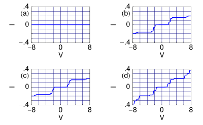
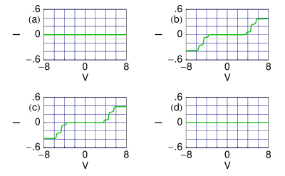
The scenario of electron transport through these molecular wires can be much more clearly explained from current-voltage (-) spectra. Current through the molecular systems is computed by the integration procedure of transmission function (see Eq. 11). The behavior of the transmission function is similar to that of the conductance spectrum since the relation is satisfied from the Landauer conductance formula. In Fig. 5, we plot - characteristics of the hydrocarbon molecules when they are connected in the trans configuration to the source and drain, where (a) and (b) correspond to the currents for the cases of weak- and strong-coupling limits, respectively. The solid, dotted, dashed and dot-dashed lines represent - curves for the benzene, napthalene, anthracene and tetracene molecules, respectively. It is observed that, in the weak-coupling limit current shows staircase-like structure with sharp steps. This is due to
the discreteness of molecular resonances as shown by the solid curves in Fig. 3. As the voltage increases, electrochemical potentials on the electrodes are shifted and eventually cross one of the molecular energy levels. Accordingly, a current channel is opened up and a jump in - curve appears. The shape and height of these current steps depend on the width of the molecular resonances. With the increase of molecule-to-electrode coupling strength, current varies almost continuously with the applied bias voltage and achieves much higher values, as shown in Fig. 5(b). This continuous variation of the current is due to the broadening of conductance resonant peaks (see the dotted curves of Fig. 3) in the strong molecule-to-electrode coupling limit.
The effect of quantum interference among the electronic waves on molecular transport is much more clearly visible from Fig. 6, where - characteristics are shown for the hydrocarbon molecules connected to the electrodes in the cis configuration. (a) and (b) correspond to the currents in the two limiting cases, respectively. The solid, dotted, dashed and dot-dashed curves give the same meaning as in Fig. 5. In this configuration (cis), current amplitude
gets reduced enormously than the case when electrodes are coupled to the molecules in the trans configuration. This enormous change in current amplitude is caused solely due to the effect of quantum interference between electronic waves passing through the molecular arms. Therefore, we can predict that designing a molecular device is significantly influenced by the quantum interference effect i.e., molecule-to-electrode interface structure.
To summarize, in this section, we have introduced a parametric approach based on a simple tight-binding model to investigate electron transport properties of four different polycyclic hydrocarbon molecules sandwiched between two D metallic electrodes. This approach can be utilized to study transport behavior in any complicated molecular bridge system. Electron conduction through the molecular wires is strongly influenced by the molecule-to-electrode coupling strength and quantum interference effect. Our investigation provides that to design a molecular electronic device, in addition to the molecule itself, both the molecular coupling and molecule-electrode interface structure are highly important.
III Designing of Classical Logic Gates
Electronic transport in quantum confined geometries has attracted much attention since these simple looking systems are the promising building blocks for designing nanodevices especially in electronic as well as spintronic engineering. The key idea of designing nano-electronic devices is based on the concept of quantum interference, and it is generally preserved throughout the sample having dimension smaller or comparable to the phase coherence length. Therefore, ring type conductors or two path devices are ideal candidates where the effect of quantum interference can be exploited san20 ; san21 ; san22 . In such a ring shaped geometry, quantum interference effect can be controlled by several ways, and most probably, the effect can be regulated significantly by tuning the magnetic flux, the so-called Aharonov-Bohm (AB) flux, that threads the ring.
In this section we will explore how a simple mesoscopic ring can be utilized to fabricate several classical logic gates. A single mesoscopic ring is used to design OR, NOT, XOR, XNOR and NAND gates, while AND and NOR gates are fabricated with the help of two such quantum rings. For all these logic gates, AB flux enclosed by a ring plays the central role and it controls the interference condition of electronic waves passing through two arms of the ring. Within a non-interacting picture, a tight-binding framework is used to describe the model and all calculations are done based on single particle Green’s function technique. The logical operations are analyzed by studying two-terminal conductance as a function of energy and current as a function of applied bias voltage. Our numerical analysis clearly supports the logical operations of the traditional macroscopic logic gates.
Here we describe two-input logic gates. The inputs are associated with externally applied gate voltages through which we can tune the strength of site energies in the atomic sites. For all logic gate operations we fix AB flux at i.e., in our chosen unit system. The common set of values of the other parameters used here are as follows. (weak-coupling limit), where and are the hopping integrals of a ring to the source and drain, respectively; and (parameters for the electrodes) and .
III.1 OR Gate
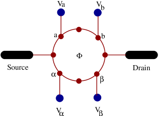
III.1.1 The model
Let us start with OR gate response. The schematic view a mesoscopic ring that can be used as an OR gate is shown in Fig. 7. The ring, penetrated by an AB flux , is symmetrically coupled (upper and lower arms have equal number of lattice points) to two semi-infinite D non-magnetic metallic electrodes, namely, source and drain. Two atomic sites and in upper arm of the ring are subject to two external
gate voltages and , respectively, and these are treated as two inputs of the OR gate. Within a non-interacting picture, the tight-binding Hamiltonian of the ring looks in the form,
| (12) |
In this Hamiltonian ’s are the site energies for all the sites except the sites and where the gate voltages and are applied, those are variable. These gate voltages can be incorporated through the site energies as expressed in the above Hamiltonian. The phase factor comes due to the flux threaded by the ring, where corresponds to the total number of atomic sites in the ring. All the other parameters have identical meaning as described earlier. In our numerical calculations, the on-site energy is taken as for all the sites , except the sites and where the site energies are taken as and , respectively, and the nearest-neighbor hopping strength in the ring is set at .
Quite interestingly we observe that, at a high output current (1) (in the logical sense) appears if one or both the inputs to the gate are high (1), while if neither input is high (1), a low output current (0) appears. This phenomenon is the so-called OR gate response and here we address it by studying conductance-energy and current-voltage characteristics as functions of magnetic flux and external gate voltages san12 .
III.1.2 Logical operation
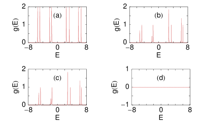
As illustrative examples, in Fig. 8 we display conductance-energy (-) characteristics for a mesoscopic ring considering in the limit of weak ring-to-electrode coupling,
where (a), (b), (c) and (d) correspond to the results for the four different cases of gate voltages and . In the particular case when i.e., both inputs are low (), conductance shows the value in the entire energy range (Fig. 8(a)). It indicates that electron cannot conduct from the source to drain across the ring. While, for the other three cases i.e., and (Fig. 8(b)), and (Fig. 8(c)) and (Fig. 8(d)), conductance shows fine resonant peaks for some particular energies associated with energy eigenvalues of the ring. Thus, in all these three cases, electron can conduct through the ring. From Fig. 8(d) it is observed that at resonances, conductance approaches the value , and hence, transmission probability goes to unity. On the other hand, it decays from for the cases where any one of the two gate voltages is high and other is low (Figs. 8(b) and (c)). Now we interpret the dependences of two gate voltages in these four different cases. The probability amplitude of getting an electron across the ring depends on the quantum interference of electronic waves passing through two arms of the ring. For symmetrically attached ring i.e., when two arms of the ring are identical to each other, the probability amplitude becomes exactly zero () at the typical flux .
This is due to the result of quantum interference among the waves passing through different arms of the ring, which can be obtained by a simple mathematical calculation. Thus for the cases when both the two inputs ( and ) are zero (low), the arms of the ring become identical, and therefore, transmission probability drops to zero. On the other hand, for the other three cases symmetry between the two arms is broken when either the atom or or the both are subject to the gate voltages and , and therefore, the non-zero value of transmission probability is achieved which reveals electron conduction across the ring. The reduction of transmission probability for the cases when any one of the two gates is high and other is low compared to the case where both are high is also due to the quantum interference effect. Thus we can predict that electron conduction takes place across the ring if any one or both the inputs to the gate are high, while if both are low, conduction is no longer possible. This feature clearly demonstrates the OR gate behavior.
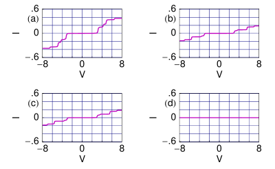
Following the above conductance-energy spectra now we describe the current-voltage characteristics. In Fig. 9 we display - curves for a mesoscopic ring with . For the case when both inputs are zero, the current is zero (see Fig. 9(a)) for the entire bias voltage . This feature is clearly visible from the conductance spectrum, Fig. 8(a), since current is computed from integration procedure of the transmission function
| Input-I () | Input-II () | Current () |
. In the other three cases, a high output current is obtained those are clearly presented in Figs. 9(b)-(d). The current exhibits staircase-like structure with fine steps as a function of applied bias voltage following the - spectrum. In addition, it is also important to note that, non-zero value of the current appears beyond a finite value of , the so-called threshold voltage (). This can be controlled by tuning the size () of the ring. From these - characteristics, OR gate response is understood very easily.
To make it much clear, in Table 1, we show a quantitative estimate of typical current amplitude determined at the bias voltage . It shows that when any one of the two gates is high and other is low, current gets the value , and for the case when both the inputs are high, it () achieves the value . While, for the case when both the two inputs are low (), current becomes exactly zero. These results clearly manifest the OR gate response in a mesoscopic ring.
III.2 AND Gate
III.2.1 The model
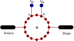
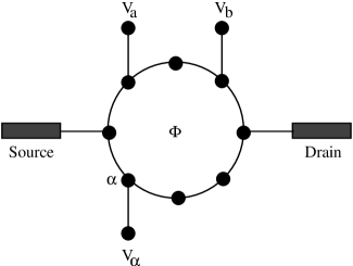
To design an AND logic gate we use two identical quantum rings those are directly coupled to each other via a single bond. The schematic view of the double quantum ring that can be used as an AND gate is presented in Fig. 10, where individual rings are penetrated by an AB flux . The double quantum ring is then attached symmetrically to two semi-infinite D metallic electrodes, namely, source and drain. Two gate electrodes, viz, gate-a and gate-b, are placed below the lower arms of the two rings, respectively, and they are ideally isolated from the rings. The atomic sites and in lower arms of the two rings are subject to gate voltages and via the gate electrodes gate-a and gate-b, respectively, and they are treated as two inputs of the AND gate. In the present scheme, we consider that the gate voltages each operate on
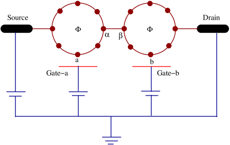
the atomic sites nearest to the plates only. While, in complicated geometric models, the effect must be taken into account for the other dots, though the effect becomes too small. The actual scheme of connections with the batteries for the operation of the AND gate is clearly presented in the figure (Fig. 10), where the source and gate voltages are applied with respect to the drain. The model quantum system is described in a similar way as prescribed in Eq. 12. We will show that, at the typical flux , a high output current () (in the logical sense) appears only if both the two inputs to the gate are high (), while if neither or only one input to the gate is high (), a low output current () results. It is the so-called AND gate response and we investigate it by studying conductance-energy and current-voltage characteristics san13 .
III.2.2 Logical operation
In Fig. 11 we plot - spectra for a double quantum ring considering (, total number of atomic sites in the double quantum ring, since each ring contains atomic sites) in the limit of weak-coupling, where (a), (b), (c) and (d) correspond to the results for four different choices of the gate voltages and , respectively. When both the two inputs and are identical to zero i.e., both are low, conductance becomes exactly zero for the entire energy range (see Fig. 11(a)). A similar response is also observed for the
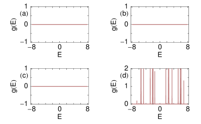
other two cases where anyone of the two inputs ( and ) to the gate is high and other one is low. The results are shown in Figs. 11(b) and (c), respectively. Thus for all these three cases (Figs. 11(a)-(c)), the double quantum ring does not allow to pass an electron from the source to drain. The conduction of electron through the bridge system is allowed only when both the two inputs to the gate are high i.e., . The response is given in Fig. 11(d), and it is observed that for some particular energies, associated with eigenenergies of the double quantum ring, conductance exhibits fine resonant peaks. Now we try to figure out the dependences of gate voltages on electron transport in these four different cases. The probability amplitude of getting an electron from the source to drain across the double quantum ring depends on the combined effect of quantum interferences of electronic waves passing through upper and lower arms of the two rings. For a symmetrically connected ring (length of the two arms of the ring are identical to each other) which is threaded by a magnetic flux , the probability amplitude of getting an electron across the ring becomes exactly zero () at the typical flux, . This is due to the result of quantum interference among the two waves in two arms of the ring, which can be shown through few simple mathematical steps. Thus for the particular case
when both inputs to the gate are low (), the upper and lower arms of the two rings become exactly identical, and accordingly, transmission probability vanishes. The similar response i.e., vanishing transmission probability, is also achieved for the two other cases (, and , ), where the symmetry is broken only in one ring out of these two by applying a gate voltage either in the site or in , preserving the symmetry in the other ring. The reason is that, when anyone of the two gates ( and ) is non-zero, symmetry between the upper and lower arms is broken only in one ring which provides non-zero transmission probability across the ring. While, for the other ring where no gate voltage is applied, symmetry between the two arms becomes preserved which gives zero transmission probability. Accordingly, the combined effect provides vanishing transmission probability across the bridge, as the rings are coupled to each other. The non-zero value of transmission probability is achieved only when the symmetries of both the two rings are identically broken. This can be done by applying gate voltages in both the sites and of the two rings. Thus for the particular case when both the two inputs are high i.e., , non-zero value of the transmission probability appears. This feature clearly demonstrates the AND gate behavior.
Now we go for the current-voltage characteristics to reveal AND gate response in a double quantum ring. As representative examples, in Fig. 12 we plot the current as a function of applied bias voltage for a double quantum ring considering in the limit of weak-coupling, where (a), (b), (c) and (d) represent the results for four different cases of the two
| Input-I () | Input-II () | Current () |
gate voltages and . For the cases when either both the two inputs to the gate are low (), or anyone of the two inputs is high and other is low (, or , ), current is exactly zero for the entire range of bias voltage. The results are shown in Figs. 12(a)-(c), and, the vanishing behavior of current in these three cases can be clearly understood from the conductance spectra Figs. 11(a)-(c). The non-vanishing current amplitude is observed only for the typical case where both the two inputs to the gate are high i.e., . The result is shown in Fig. 12(d). From this current-voltage curve we see that the non-zero value of the current appears beyond a finite value of , the so-called threshold voltage (). This can be controlled by tuning the size () of the two rings. From these results, the behavior of AND gate response is clearly visible.
In the same fashion as earlier here we also make a quantitative estimate for the typical current amplitude as given in Table 2, where the typical current amplitude is measured at the bias voltage . It shows only when two inputs to the gate are high (), while for the other three cases when either or , or , , current gets the value . It verifies the AND gate behavior in a double quantum ring.
III.3 NOT Gate
III.3.1 The model
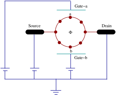
Next we discuss NOT gate operation in a quantum ring san14 . Schematic view for the operation of a NOT gate using a single mesoscopic ring is shown in Fig. 13, where the ring is attached symmetrically to two semi-infinite D metallic electrodes, viz, source and drain, and it is subject to an AB flux .
A gate voltage , taken as input voltage of the NOT gate, is applied to the atomic site in upper arm of the ring. While, an additional gate voltage is applied to the site in lower arm of the ring. Keeping to a fixed value, we change properly to achieve the NOT gate operation. The model quantum system is illustrated in the same way as given in Eq. 12. We will verify that, at the typical flux , a high output current () (in the logical sense) appears if the input to the gate is low (), while a low output current () appears when the input to the gate is high (). This phenomenon is the so-called NOT gate behavior, and we will explore it following the same prescription as earlier.
III.3.2 Logical operation
To describe NOT gate operation let us start with conductance-energy characteristics. In Fig. 14 we show the variation of conductance as a function of injecting electron energy, in the limit of weak-coupling, for a mesoscopic ring with and . Figures 14(a) and (b) correspond to the results for the input voltages and , respectively. For the particular case when the input voltage i.e., the input is high, conductance vanishes (Fig. 14(b)) in the complete
energy range. This indicates that conduction of electron from the source to drain through the ring is not possible. The situation becomes completely different for the case when the input to the gate is zero (). The result is shown in Fig. 14(a), where conductance shows sharp resonant peaks for some fixed energies associated with energy eigenvalues of the ring. This reveals electron conduction across the ring. Now we focus the dependences of gate voltages on electron transport for two different cases of the input voltage. For the case when the input to the gate is equal to i.e., , the upper and lower arms of the ring become exactly similar. This is because the potential is also set to . Therefore, transmission probability drops to zero at the typical flux , as discussed earlier. Now if the input voltage is different from the potential applied in the atomic site , then the two arms are not identical with each other and transmission probability will not vanish. Thus, to get zero transmission probability when the input is high, we should tune properly, observing the input potential and vice versa. On the other hand, due to the breaking of symmetry between the two arms, non-zero value of the transmission probability is achieved in the particular case where the input voltage is zero (), which reveals electron conduction across the ring. From these results we can emphasize
that electron conduction takes place through the ring if the input to the gate is zero, while if the input is high, conduction is no longer possible. This aspect clearly describe the NOT gate behavior.
To illustrate the current-voltage characteristics now we concentrate on the results given in Fig. 15. The currents are drawn as a function of applied bias voltage for a mesoscopic ring with and in the weak-coupling limit, where (a) and (b) represent the results for two choices of the input signal . Clearly we see that, when the input to the gate is identical to (high), current becomes exactly zero (see Fig. 15(b)) for the entire bias voltage . This feature is understood from the conductance spectrum, Fig. 14(b). On the other hand, a non-zero value of current is obtained when the input voltage , as given in Fig. 15(a). The current becomes non-zero beyond a threshold voltage which is tunable depending on the ring size and ring-electrode coupling strength. From these current-voltage curves it is clear that a high output current appears only if the input to the gate is low, while for high input, current doesn’t appear. It justifies NOT gate response in the quantum ring.
In a similar way, as we have studied earlier in other logical operations, in Table 3 we make a quantitative measurement of the typical current amplitude for the quantum ring. The current amplitude is computed at the bias voltage . It shows that, when the input to the gate
| Input () | Current () |
|---|---|
is zero, current gets the value . While, current becomes exactly zero when the input voltage . Thus the NOT gate operation by using a quantum ring is established.
Up to now we have studied three primary logic gate operations using one (OR and NOT) and two (AND) mesoscopic rings. In the forthcoming sub-sections we will explore the other four combinatorial logic gate operations using such one or two rings.
III.4 NOR Gate
III.4.1 The model
We begin by referring to Fig. 16. A double quantum ring, where each ring is threaded by a magnetic flux , is sandwiched symmetrically between two semi-infinite one-dimensional (D) metallic electrodes. The atomic sites and in lower arms of the two rings are subject to gate voltages and through the gate electrodes gate-a and gate-b, respectively. These gate voltages are variable and treated as two inputs of the NOR gate. In a similar way we also apply two other gate voltages and , those are not varying, in the atomic sites and in upper arms of the two rings via the gate electrodes gate-c and gate-d, respectively. All these gate electrodes are ideally isolated from the rings, and here we assume that the gate voltages each operate on the atomic sites nearest to the plates only. While, in complicated geometric models, the effect must be taken into account for other atomic sites, though the effect becomes too small. The actual
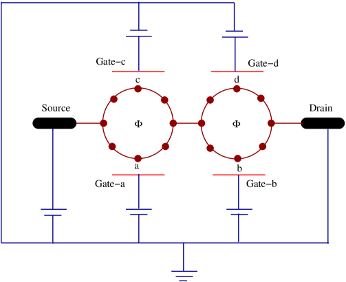
scheme of connections with the batteries for the operation of a NOR gate is clearly presented in the figure (Fig. 16), where the source and gate voltages are applied with respect to the drain. The tight-binding Hamiltonian of the model quantum system is described in a similar fashion as given in Eq. 12. Keeping and to some specific values, we regulate and properly to achieve NOR gate operation. Quite nicely we establish that, at the typical AB flux , a high output current () (in the logical sense) appears if both inputs to the gate are low (), while if one or both are high (), a low output current () results. This phenomenon is the so-called NOR gate response and we will illustrate it by describing conductance-energy and current-voltage characteristics san15 .
III.4.2 Logical operation
As representative examples, in Fig. 17 we display the variation of conductance as a function of injecting electron energy for a double quantum ring with (, total number of atomic sites in the double quantum ring, since each ring contains atomic sites) in the weak-coupling limit, where (a), (b), (c) and (d) represent the results for four different cases of the gate voltages and , respectively. Quite interestingly from these spectra we observe that, for the case when both the two inputs and are identical to i.e., both are high, conductance becomes exactly zero for the full range of energy (see Fig. 17(d)). An exactly similar response is also visible for other two cases where anyone of the two inputs is high and other is low. The results are shown in Figs. 17(b) and (c), respectively. Hence, for all these three cases (Figs. 17(b)-(d)), no electron conduction takes place from the source to drain through the double quantum ring. The electron conduction through the bridge system is allowed
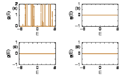
only for the typical case where both the inputs to the gates are low i.e., . The spectrum is given in Fig. 17(a). It is noticed that, for some particular energies conductance exhibits sharp resonant peaks associated with energy levels of the double quantum ring. Now we try to explain the roles of the gate voltages on electron transport in these four different cases. The probability amplitude of getting an electron from the source to drain across the double quantum ring depends on the combined effect of quantum interferences of the electronic waves passing through upper and lower arms of the two rings. For the particular case when both the two inputs to the gate are high i.e., , upper and lower arms of the two rings become exactly identical since the gate voltages and in the upper arms are also fixed at the value . This provides the vanishing transmission probability. If the input voltages and are different from the potential applied in the atomic sites and , then the upper and lower arms of the two rings are no longer identical to each other and transmission probability will not vanish. Thus, to get zero transmission probability when the inputs are high, we should tune and properly, observing the input potentials and vice versa. A similar behavior is also noticed for the other two cases (, and , ), where symmetry is broken in only one ring out of these two by making the gate voltage either in the site or in to zero, maintaining the symmetry in other ring. The reason is that, when anyone of the two gates ( and ) becomes zero, symmetry between the upper and lower arms is broken only in one ring which provides
non-zero transmission probability across the ring. While, for the other ring where the gate voltage is applied, symmetry between the two arms becomes preserved which gives zero transmission probability. Accordingly, the combined effect of these two rings provides vanishing transmission probability across the bridge, as the rings are coupled to each other. The non-zero value of transmission probability appears only when symmetries of both the two rings are identically broken, and it is available for the particular case when two inputs to the gate are low i.e., . This feature clearly demonstrates the NOR gate behavior.
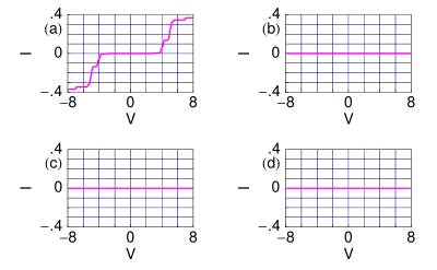
To support NOR gate operation now we focus our mind on the - characteristics. As illustrative examples, in Fig. 18 we show the variation of current as a function of applied bias voltage for a double quantum ring with in the limit of weak-coupling, where (a), (b), (c) and (d) correspond to the results for the different cases of two input voltages, respectively. For the cases when either both the two inputs to the gate are high (), or anyone of the two inputs is high and other is low (, or , ), current drops exactly to zero for the whole range of bias voltage. The results are shown in Figs. 18(b)-(d), and, the vanishing behavior of current in these three different cases can be clearly
| Input-I () | Input-II () | Current () |
understood from conductance spectra given in Figs. 17(b)-(d). The finite value of current is observed only for the typical case where both the two inputs to the gate are low i.e., . The result is shown in Fig. 18(a). At much low bias voltage, current is almost zero and it shows a finite value beyond a threshold voltage depending on the ring size ans ring-to-electrode coupling strength. These features establish the NOR gate response.
For the sake of our completeness, in Table 4 we do a quantitative measurement of the typical current amplitude, determined at , for four different choices of two input signals in the limit of weak-coupling. Our measurement shows that current gets a finite value () only when both inputs are low (). On the other hand, current becomes zero for all other cases i.e., if one or both inputs are high. Therefore, it is manifested that a double quantum ring can be used as a NOR gate.
III.5 XOR Gate
III.5.1 The model
As a follow up, now we address XOR gate response which is designed by using a single mesoscopic ring san16 . The ring, penetrated by an AB flux ,
is attached symmetrically to two semi-infinite D non-magnetic metallic electrodes, namely, source and drain. The ring is placed between two gate electrodes, viz, gate-a and gate-b. These gate electrodes are ideally isolated from the ring and can be regarded as two parallel plates of a capacitor. In our present scheme we assume that the gate voltages each operate on the dots nearest to the plates only. While, in complicated geometric models, the effect must be taken into account for the other dots, though the effect becomes too small. The dots and in two arms of the ring are subject to gate voltages and , respectively, and these are treated as two inputs of the XOR gate. The actual scheme of connections with the batteries for the operation of the XOR gate is clearly presented in the figure (Fig. 19), where the source and gate voltages are applied with respect to the drain. We describe the model quantum system through a similar kind of tight-binding Hamiltonian as presented in Eq. 12. Very nicely we follow that, at the typical AB flux , a high output current () (in the logical sense) appears if one, and only one, of the inputs to the gate is high (), while if both inputs are low () or both are high (), a low output current () results. This is the so-called XOR gate behavior and we will emphasize it according to our earlier prescription.
III.5.2 Logical operation
Let us start with conductance-energy characteristics given in Fig. 20. The variations of conductances are shown as a function of injecting electron energy for a quantum ring considering in the weak ring-to-electrode coupling limit, where four different figures correspond to the results for different choices of two input signals and . When both the two inputs and are identical to zero i.e., both inputs are low, conductance becomes exactly zero (Fig. 20(a)) for all energies. This reveals that electron cannot conduct through the ring. A similar response is also
observed when both the two inputs are high i.e., , and in this case also the ring does not allow to pass an electron from the source to drain (Fig. 20(d)). On the other hand, for the cases where any one of the two inputs is high and other is low i.e., either and (Fig. 20(b)) or and (Fig. 20(c)), conductance exhibits fine resonant peaks for some particular energies associated with energy levels of the ring. Thus for both these two cases electron conduction takes place across the ring. Now we justify the dependences of gate voltages on electron transport for these four different cases. For the cases when both inputs ( and ) are either low or high, the upper and lower arms of the ring are exactly similar in nature, and therefore, at transmission probability drops exactly to zero. On the other hand, for the other two cases symmetry between the arms of the ring is broken by applying a gate voltage either in the atom or , and therefore, the non-zero value of transmission probability is achieved which reveals electron conduction across the ring. Thus we can predict that electron conduction takes place across the ring if one, and only one, of the inputs to the gate is
high, while if both inputs are low or both are high, conduction is no longer possible. This phenomenon illustrates the traditional XOR gate behavior.
With these conductance-energy spectra (Fig. 20), now we focus our attention on current-voltage characteristics. As illustrative examples, in Fig. 21 we show current-voltage characteristics for a mesoscopic ring with in the limit of weak-coupling. For the cases when both the two inputs are identical
| Input-I () | Input-II () | Current () |
to each other, either low (Fig. 21(a)) or high (Fig. 21(d)), current becomes zero for the entire bias voltage. This behavior is clearly understood from the conductance spectra, Figs. 20(a) and (d). For the other two cases where only one of the two inputs is high and other is low, a high output current is obtained which are clearly described in Figs. 21(b) and (c). The finite value of current appears when the applied bias voltage crosses a limiting value, the so-called threshold bias voltage . Thus to get a current across the ring, we have to take care about the threshold voltage. These results implement the XOR gate response in a mesoscopic ring.
To make an end of the discussion for XOR gate response in a more compact way in Table 5 we make a quantitative measurement of typical current amplitude for the four different cases of two input signals. The current amplitudes are computed at the bias voltage . It is observed that current becomes zero when both inputs are either low or high. While, it (current) reaches the value when we set one input as high and other as low. These studies suggest that a mesoscopic ring can be used as a XOR gate.
III.6 XNOR Gate
III.6.1 The model
As a consequence now we will explore XNOR gate response and we design this logic gate by means of a single mesoscopic ring san17 . The ring, threaded by an AB flux , is attached symmetrically (upper and lower arms have equal number of lattice points) to two semi-infinite one-dimensional (D) metallic electrodes. The model quantum system is schematically shown in Fig. 22. Two gate voltages and , taken as two inputs of the XNOR gate, are applied to the atomic sites and , respectively, in upper arm of the ring. While, an additional gate voltage is applied to the site in lower arm of the ring. These three voltages are variable. Our quantum system is described by a similar kind of Hamiltonian given in Eq. 12. We show that, at the typical magnetic flux a high output current () (in the logical sense) appears if both the two inputs to the gate are the same, while if one but not both inputs are high (), a low
output current () results. This logical operation is the so-called XNOR gate behavior and we will focus it by studying conductance-energy spectrum and current-voltage characteristics for a typical mesoscopic ring.
III.6.2 Logical operation
As illustrative examples, in Fig. 23 we describe conductance-energy (-) characteristics for a mesoscopic ring with and in the limit of weak-coupling, where (a), (b), (c) and (d) correspond to the results for different cases of the input voltages, and . For the particular cases where anyone of the two inputs is high and other is low i.e., both inputs are not same, conductance becomes exactly zero (Figs. 23(b) and (c)) for the whole energy range. This predicts that for these two cases, electron cannot conduct through the ring. The situation becomes completely different for the cases when both the inputs to the gate are same, either low () or high (). In these two cases, conductance exhibits fine resonant peaks for some particular energies (Figs. 23(a) and (d)), which reveals electron conduction across the ring. At the resonant energies, does not get the value , and therefore, transmission probability becomes less than unity, since the expression is satisfied from the Landauer conductance formula (see Eq. 1 with ). This reduction of transmission amplitude is due to the effect of quantum interference. Now we discuss the effect of gate voltages on electron transport for these four different cases of the input voltages. For the cases when anyone of the two inputs to the gate is identical to
and other one is , the upper and lower arms of the ring become exactly similar. This is because the potential is also set

to . Accordingly, transmission probability drops to zero. If the high value () of anyone of the two gates is different from the potential applied in the atomic site , then two arms are not identical with each other and transmission probability will not vanish. Thus, to get zero transmission probability when is high and is low and vice versa, we should tune properly, observing the input potential. On the other hand, due to the breaking of symmetry of the two arms, non-zero value of the transmission probability is achieved in the particular cases when both inputs to the gate are same, which reveals electron conduction across the ring. From these results we can emphasize that electron conduction through the ring takes place if both the two inputs to the gate are the same (low or high), while if one but not both inputs are high, conduction is no longer possible. This aspect clearly describes the XNOR gate behavior.
As a continuation now we follow current-voltage characteristics to reveal the XNOR gate response. As representative examples, in Fig. 24 we plot - characteristics for a mesoscopic ring with and , in the limit of weak-coupling, where (a), (b), (c) and (d) represent the results for four different cases of the two input voltages. From these characteristics it is clearly observed that for the cases when one input is high and other is low,
| Input-I () | Input-II () | Current () |
current is exactly zero (see Figs. 24(b) and (c)) for the entire bias voltage . This phenomenon can be understood from the conductance spectra, Figs. 23(b) and (c). The non-zero value of current appears only when both the two inputs are identical to zero (Fig. 24(a)) or high (Fig. 24(d)). Here also the current appears beyond a finite threshold voltage which is regulated under the variation of system size and ring-electrode coupling strength. These - curves justify the XNOR gate response in a mesoscopic ring.
To be more precise, in Table 6 we make a quantitative measurement of typical current amplitude for the different choices of two input signals in the weak ring-to-electrode coupling. The typical current amplitude is computed at the bias voltage . It is noticed that current gets the value when both inputs are low (), while it becomes when both inputs to the gate are high (). On the other hand for all other cases, current is always zero. These results emphasize that a mesoscopic ring can be used to design a XNOR gate.
III.7 NAND Gate
III.7.1 The model
At the end, we demonstrate NAND gate response and we design this logic gate with the help of a single mesoscopic ring. A mesoscopic ring, threaded by a magnetic flux , is attached symmetrically (upper and lower arms have equal number of lattice points) to two semi-infinite
one-dimensional (D) metallic electrodes. The schematic view of the ring that can be used to design a NAND gate is shown in Fig. 25. In upper arm of the ring two atoms and are subject to gate voltages and , respectively, those are treated as two inputs of the NAND gate. On the other hand, two additional voltages and are applied in the atoms and , respectively, in lower arm of the ring. The model quantum system is expressed by a similar kind of tight-binding Hamiltonian as prescribed in Eq. 12. Quite interestingly we notice that, at the typical AB flux a high output current () (in the logical sense) appears if one or both inputs to the gate are low (), while if both inputs to the gate are high (), a low output current () results. This characteristic is the so-called NAND gate response and we will justify it by describing conductance-energy and current-voltage spectra san18 .
III.7.2 Logical operation
Let us begin with the results given in Fig. 26. Here we show the variation of conductance () as a function of injecting electron energy () in the limit of weak-coupling for a mesoscopic ring with and , where (a), (b), (c) and (d) correspond
to the results for the different values of and . When both the two inputs and are identical to i.e., both inputs are high, conductance becomes exactly zero (Fig. 26(d)) for all energies. This reveals that electron cannot conduct from the source to drain through the ring. While, for the cases where anyone or both inputs to the gate are zero (low), conductance gives fine resonant peaks for some particular energies associated with energy levels of the ring, as shown in Figs. 26(a), (b) and (c), respectively. Thus, in all these three cases, electron can conduct through the ring. From Fig. 26(a) it is observed that, at resonances reaches the value (), but the height of resonant peaks gets down () for the cases where anyone of the two inputs is high and other is low (Figs. 26(b) and (c)). Now we illustrate the dependences of gate voltages on electron transport for these four different cases. For the case when both inputs to the gate are identical to i.e., , the upper and lower arms of the ring become exactly similar. This is due to the fact that the potentials and are also fixed to . Therefore, in this particular case transmission probability drops to zero at . If the two inputs and are different from the potentials applied in the sites and , then two arms are no longer identical to each other and transmission probability will not vanish. Hence, to get zero transmission probability when both inputs are high, we should tune and properly, observing the input potentials and vice versa. On the other hand, due to breaking of the symmetry of the two arms (i.e., two arms are no longer identical to each other) in the other
three cases by making anyone or both inputs to the gate are zero (low), the non-zero value of transmission probability is achieved which reveals electron conduction across the ring. The reduction of transmission probability from unity for the cases where any one of the two gates is high and other is low compared to the case where both the gates are low is solely due to the quantum interference effect. Thus it can be emphasized that electron conduction takes place across the ring if any one or both inputs to the gate are low, while if both are high, conduction is not at all possible. These results justify the traditional NAND gate operation.
In the same fashion, now we focus on the current-voltage characteristics. As our illustrative purposes, in Fig. 27 we present the variation of current in terms of applied bias voltage for a typical quantum ring with in the limit of weak-coupling, considering , where (a)-(d) represent the results for different cases of two input signals. When both inputs are high i.e, current becomes zero for the entire range of applied bias voltage (Fig. 27(d)), following the conductance-energy spectrum given in Fig. 26(d). For all other three choices of two inputs, finite contribution in the current is available. The results are shown in Figs. 27(a)-(c). From these three current-voltage spectra, it is observed that for a fixed bias voltage current amplitude in the typical case where both inputs are low (Fig. 27(a)) is much higher than the cases where one input is high and other is low (Figs. 27(b)-(c)). This is clearly understood from the variations of conductance-energy spectra studied in the above paragraph. Thus, our present current-voltage characteristics justify the NAND gate operation in the quantum ring very nicely.
Finally, in Table 7 we present a quantitative estimate of the typical current amplitude for four different cases of two input signals. The typical current amplitudes are measured at the bias voltage
| Input-I () | Input-II () | Current () |
. It provides that current vanishes when both inputs are high (). On the other hand, current gets the value as long as both inputs are low () and when anyone of two inputs is low and other is high. Our results support that a mesoscopic ring can be utilized as a NAND gate.
To summarize, in this section, we have implemented classical logic gates like OR, AND, NOT, NOR, XOR, XNOR and NAND using simple mesoscopic rings. A single ring is used to design OR, NOT, XOR, XNOR and NAND gates, while the rest two gates are fabricated by using two such rings and in all the cases each ring is penetrated by an AB flux which plays the crucial role for whole logic gate operations. We have used a simple tight-binding framework to describe the model, where a ring is attached to two semi-infinite one-dimensional non-magnetic metallic electrodes. Based on a single particle Green’s formalism all calculations have been done numerically which demonstrate two-terminal conductance and current through the system. Our theoretical analysis may be useful in fabricating mesoscopic or nano-scale logic gates.
Throughout the study of logic gate operations using mesoscopic rings, we have chosen the rings of two different sizes. In few cases we have considered the ring with atomic sites and in few cases the number is . In our model calculations, these typical numbers ( or ) are chosen only for the sake of simplicity. Though the results presented here change numerically with ring size (), but all the basic features remain exactly invariant. To be more specific, it is important to note that, in real situation experimentally achievable rings have typical diameters within the range - m. In such a small ring, unrealistically very high magnetic fields are required to produce a quantum flux. To overcome this situation, Hod et al. have studied extensively and proposed how to construct nanometer scale devices, based on Aharonov-Bohm interferometry, those can be operated in moderate magnetic fields hod1 ; hod2 .
The importance of this study is mainly concerned with (i) simplicity of the geometry and (ii) smallness of the size.
IV Multi-terminal quantum transport
Though, to date a lot of theoretical as well as experimental works on two-terminal electron transport have been done addressing several important issues, but a very few works are available on multi-terminal quantum systems xu1 ; ember ; let ; zhong ; lin ; sumit1 and still it is an open subject to us. Büttiker butt2 first addressed theoretically the electron transport in multi-terminal quantum systems following the theory of Landauer two-terminal conductance formula.
In this section we investigate multi-terminal quantum transport through a single benzene molecule attached to metallic electrodes. A simple tight-binding model is used to describe the system and all calculations are done based on the Green’s function formalism. Here we address numerical results which describe multi-terminal conductances, reflection probabilities and current-voltage characteristics. Most significantly we observe that, the molecular system where a benzene molecule is attached to three terminals can be operated as a transistor, and we call it a molecular transistor san19 . This aspect can be utilized in designing nano-electronic circuits and our investigation may provide a basic framework to study electron transport in any complicated multi-terminal quantum system.
IV.1 Model and synopsis of the theoretical background
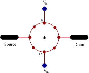
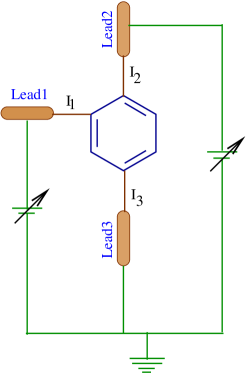
Following the prescription of electron transport in two-terminal quantum systems (as illustrated in section II) we can easily extend our study in a three-terminal quantum system, where a benzene molecule is attached to three semi-infinite leads, viz, lead-1, lead-2 and lead-3. The model quantum system is shown in Fig. 28.
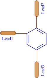
These leads are coupled to the molecule asymmetrically and they are quite analogous to emitter, base and collector as defined in a traditional macroscopic transistor. The actual scheme of connections with the batteries for the operation of the molecule as a transistor is depicted in Fig. 29, where the voltages in the lead- and lead- are applied with respect to lead-. In non-interacting picture, the Hamiltonian of the benzene molecule can be expressed like,
| (13) |
where the symbols have their usual meaning. A similar kind of tight-binding Hamiltonian is also used to describe the side-attached leads which is parametrized by constant on-site potential and nearest-neighbor hopping integral . We use three other parameters , and to describe hopping integrals of the molecule to the lead-, lead- and lead-, respectively.
To calculate conductance in this three-terminal quantum system, we use Büttiker formalism, where all leads (current and voltage leads) are treated in the same footing. The conductance between the terminals,
indexed by and , can be written by the relation , where gives the transmission probability of an electron from the lead- to lead-. Here, reflection probabilities are related to the transmission probabilities by the equation , which is obtained from the condition of current conservation xu .
Finally, for this three-terminal system we can write the current for the lead- as,
| (14) |
Here, all the results are computed only at absolute zero temperature. These results are also valid even for some finite (low) temperatures, since the broadening of energy levels of the benzene molecule due to its coupling to the leads becomes much larger than that of the thermal broadening datta1 ; datta2 . For the sake of simplicity, we take the unit in our present calculations.
IV.2 Numerical results and discussion
To illustrate the results, let us begin our discussion by mentioning the values of different parameters used for the numerical calculations. In the benzene molecule, on-site energy is fixed to for all the sites and nearest-neighbor hopping strength is set to . While, for the side-attached leads on-site energy () and nearest-neighbor hopping strength () are chosen as and , respectively. The Fermi energy is taken as . Throughout the study, we narrate our results for two limiting cases depending on the strength of coupling of the molecule to leads. Case I: . It is the so-called weak-coupling limit. For this regime we choose . Case II: . This is the so-called strong-coupling limit. In this particular limit, we set the values of the parameters as .
IV.2.1 Conductance-energy characteristics
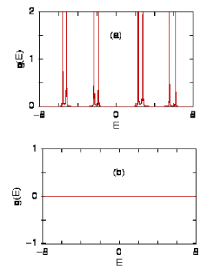
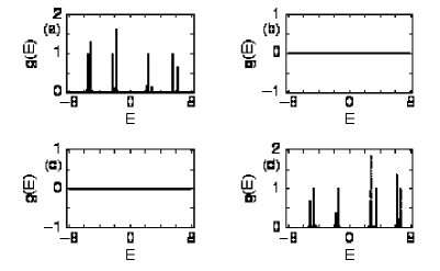
In three-terminal molecular system, several anomalous features are observed in conductance-energy spectra as well as in the variation of reflection probability with energy . As representative examples, in Fig. 30 we present the results, where first column gives the variation of conductance and second column represents the nature of reflection probability . From the conductance spectra it is observed that conductances exhibit fine resonant peaks (red curves) for some particular energies in the limit of weak-coupling, while they get broadened (blue curves) as long as coupling strength is enhanced to the strong-coupling limit. The explanation for the broadening of resonant peaks is exactly similar as described earlier in the case of two-terminal molecular system. A similar effect of molecular coupling to the side attached leads is also noticed in the variation of reflection probability versus energy spectra (right column of Fig. 30). Since in this three-terminal molecular system leads are connected asymmetrically to the molecule i.e., path length between the leads are different from each other, all conductance spectra are different in nature. It is also observed that the heights of different conductance peaks are not identical. This is solely due to the effect of quantum interference among different arms of the molecular ring. Now, in the variation of reflection probabilities, we also get the complex structure like as conductance spectra. For this three-terminal system since reflection
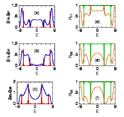
probability is not related to the transmission probability simply as in the case of a two-terminal system, it is not necessarily true that shows picks or dips where has dips or picks. It depends on the combined effect of ’s.
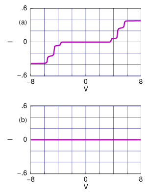
IV.2.2 Current-voltage characteristics: Transistor operation
Finally, we describe current-voltage characteristics for this three-terminal molecular system and try to illustrate how it can be operated as a transistor.
The current passing through any lead- is obtained by integration procedure of the transmission function (see
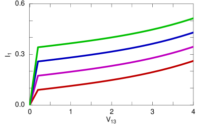
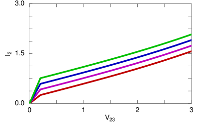
Eq. (14)), where individual contributions from the other two leads have to be taken into account. To be more precise, we can write the current expression for the three-terminal molecular device where one of the terminals serves as a voltage as well as a current probe datta1 in the form , where is the voltage difference between the lead- and lead-.
In Fig. 31, we plot current in the lead- as a function of for constant in the limit of strong molecular coupling. The red, magenta, blue and green curves correspond to the currents for , , and , respectively. From the results it is observed that, for a constant voltage difference between the lead- and lead-, current initially rises to a large value when starts to increase from zero value, and after that, it () increases very slowly with the rise of and eventually saturates. On the other hand, for a constant lead- to lead- voltage difference, current increases gradually as we increase , which is clearly described from the four different curves in Fig. 31. Quite similar behavior is also observed in the variation of current as a function of for constant . The results are shown in Fig. 32, where currents are calculated for the strong-coupling limit. The red, magenta, blue and green lines represent the currents for , , and , respectively. Comparing the
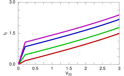
results plotted in Figs. 31 and 32, it is clearly observed that current in the lead- is much higher than the current available in the lead- for the entire voltage range. This is solely due to the effect of quantum interference among the electronic waves passing through different arms of the molecular ring, and, we can manifest that for a fixed molecular coupling, current amplitude significantly depends on the positions of different leads.
At the end, we illustrate the results plotted in Fig. 33, where the variation of current is shown as a function of for constant current . The currents () are calculated for the strong-coupling limit, where the red, green, blue and magenta curves correspond to fixed , , and , respectively. For a constant , current through the lead- increases gradually as we increase the current which is clearly visible from the four different curves in this figure. These current-voltage characteristics are quite analogous to a macroscopic transistor. Thus, in short, we can predict that this three-terminal molecular system can be operated as a transistor and we may call it a molecular transistor. Like a conventional macroscopic transistor, the three different terminals of the molecular transistor can be treated as emitter, base and collector. Here, the important point is that, since all these three terminals are equivalent to each other, any one of them can be considered as an emitter or base or collector. Not only that, for this molecular transistor as there is only one type of charge carrier, which is electron, conventional biasing method is not required. These features provide several key ideas which motivate us to develop a molecular transistor rather than the traditional one.
All the above current-voltage characteristics for the three-terminal quantum system are studied only for the limit of strong molecular coupling. Exactly similar features, except the current amplitude, are also observed for the case of weak-coupling limit, and in obvious reason here we do not plot these results once again.
To summarize, in this section, we have explored electron transport through a benzene molecule attached to metallic electrodes. The molecular system is described by a simple tight-binding Hamiltonian and all calculations are done through Green’s function approach. We have numerically calculated the multi-terminal conductances, reflection probabilities and current-voltage characteristics. Very interestingly we have seen that the three-terminal benzene molecule can be operated as an electronic transistor, and we call it as a molecular transistor. These three terminals are analogous to emitter, base and collector as defined in traditional transistor. All these features of electron transport may be utilized in fabricating nano-electronic devices and our detailed investigation can provide a basic theoretical framework to characterize electron transport in any complicated multi-terminal quantum system.
Here we have made some minor approximations in considering the site energies of carbon-type sites and the nearest-neighbor hopping strength between these sites in molecular ring. The absolute value of nearest-neighbor hopping strength () alternates between the two values, those are respectively taken as and low . Here we have approximated it () to the absolute value . With this assumption, the characteristic features are not changed at all. On the other hand, the absolute value of on-site energy () corresponding to carbon-type sites in this molecule is identical to low . But here we have set it to zero, only for the sake of simplicity, since the constant value of on-site energy simply gives the shift of energy eigenvalues and hence transmission spectra, keeping the current-voltage characteristics unchanged. The main motivation of considering a benzene molecule to reveal the transistor operation is that molecular systems are ideal candidates for future development of nano-electronic devices. Here we have done a model calculation considering a benzene molecule and presented the results for these set of parameter values. Instead of a benzene molecule one can also take a mesoscopic ring and perform all the calculations for other set of parameter values. In that situation, only the results presented here change numerically with the ring size, but all the basic features remain exactly invariant.
V Summary and Conclusions
In this review article we have demonstrated some important issues on electron transport through some model quantum systems. With a brief introduction of several fundamental issues in mesoscopic region, we have investigated electron transport through four different polycyclic hydrocarbon molecules, namely, benzene, napthalene, anthracene and tetracene. A tight-binding framework is used to describe the model quantum systems and all calculations are performed using Green’s function technique. Electron conduction through these molecular wires is significantly influenced by the molecule-to-electrode coupling strength and quantum interference of electronic waves passing through different arms of the molecular ring. Our numerical results predict that to design a molecular electronic device, not only the molecule, both the molecular coupling to side attached electrodes and molecule-electrode interface structure are highly important. Our model calculations provide a physical insight to the behavior of electron conduction through molecular bridge systems.
In the next part we have illustrated the possibilities of designing classical logic gates using simple mesoscopic rings. First we have studied three primary logic gate operations using one (OR and NOT) and two (AND) quantum rings. Later, we have established other four combinatorial logic gate operations (NOR, XOR, XNOR and NAND) using such one or two rings. The key controlling parameter for all logic gate operations is the magnetic flux threaded by the ring. The logical operations have been described in terms of conductance-energy and current-voltage characteristics. Our analysis may be useful in fabricating meso-scale or nano-scale logic gates.
In the last part of this review article, we have discussed about multi-terminal transport problem. In a multi-terminal quantum system electron transport cannot be addressed by using Landauer approach. Büttiker first resolved this issue considering Landauer two-terminal transport formula and the technique has been named as Landauer-Büttiker approach. Using this methodology we have studied multi-terminal quantum transport through a single benzene molecule. Our numerical results describe multi-terminal conductances, reflection probabilities and current-voltage characteristics. Quite interestingly we have shown that the three-terminal benzene molecule can be operated as an electronic transistor. These three terminals are analogous to the emitter, base and collector as defined in conventional transistor. Our presented results may provide a basic theoretical framework to address electron transport in any multi-terminal quantum system.
References
- (1) Y. Imry. Introduction to Mesoscopic Physics. Oxford University Press, New York (1997).
- (2) S. Datta, Electronic transport in mesoscopic systems, Cambridge University Press, Cambridge (1995).
- (3) S. Datta, Quantum Transport: Atom to Transistor, Cambridge University Press, Cambridge (2005).
- (4) G. Metalidis, Electronic Transport in Mesoscopic Systems. PhD thesis, Martin-Luther-Universität Halle-Wittenberg (2007).
- (5) D. Weinmann, The Physics of Mesoscopic Systems, (2005), based on the Lectures held during the Seventh Petra School of Physics during 17-22 September 2000 at the University of Jordon.
- (6) S. Washburn and R. A. Webb, Adv. Phys. 35, 375 (1986).
- (7) R. A. Webb and S. Washburn, Physics Today 41, 46 (1988).
- (8) A. B. Fowler, A. Hartstein, and R. A. Webb, Phys. Rev. Lett. 48, 196 (1982).
- (9) P. A. Lee, A. D. Stone, and H. Fukuyama, Phys. Rev. B 35, 1039 (1987).
- (10) M. Büttiker, Y. Imry, and R. Landauer, Phys. Lett. A 96, 365 (1983).
- (11) L. P. Levy, G. Dolan, J. Dunsmuir, and H Bouchiat, Phys. Rev. Lett. 64, 2074 (1990).
- (12) D. Mailly, C. Chapelier, and A. Benoit, Phys. Rev. Lett. 70, 2020 (1993).
- (13) V. Chandrasekhar, R. A. Webb, M. J. Brady, M. B. Ketchen, W. J. Gallagher, and A. Kleinsasser, Phys. Rev. Lett. 67, 3578 (1991).
- (14) E. M. Q. Jariwala, P. Mohanty, M. B. Ketchen, and R. A. Webb, Phys. Rev. Lett. 86, 1594 (2001).
- (15) R. Deblock, R. Bel, B. Reulet, H. Bouchiat, and D. Mailly, Phys. Rev. Lett. 89, 206803 (2002).
- (16) M. Büttiker, Phys. Rev. B 32, 1846 (1985).
- (17) H-F Cheung, E. K. Riedel, and Y. Gefen, Phys. Rev. Lett. 62, 587 (1989).
- (18) H. F. Cheung, Y. Gefen, E. K. Riedel, and W. H. Shih, Phys. Rev. B 37, 6050 (1988).
- (19) H. Bluhm, N. C. Koshnick, J. A. Bert, M. E. Huber, and K. A. Moler, Phys. Rev. Lett. 102, 136802 (2009).
- (20) S. K. Maiti, Physica E 31, 117 (2006).
- (21) S. K. Maiti, Int. J. Mod. Phys. B 21, 179 (2007).
- (22) S. K. Maiti, Int. J. Mod. Phys. B 22, 4951 (2008).
- (23) S. K. Maiti, Solid State Phenomena 155, 87 (2009).
- (24) S. K. Maiti, Solid State Commun. 150, 2212 (2010).
- (25) Y. Aharonov and D. Bohm, Phys. Rev. 115, 485 (1959).
- (26) K. von Klitzing, G. Dorda, and M. Pepper, Phys. Rev. Lett. 45, 494 (1980).
- (27) R. E. Prange and S. M. Girvin. The Quantum Hall Effect. Springer-Verlag, New York (1987).
- (28) T. Chakraborty and P. Pietiläinen. The Quantum Hall Effects. Solid-State Sciences. Springer, Berlin, second edition (1995).
- (29) D. C. Tsui, H. L. Stormer, and A. C. Gossard, Phys. Rev. Lett. 48, 1559 (1982).
- (30) R. B. Laughlin, Phys. Rev. Lett. 50, 1395 (1983).
- (31) R. Landauer, IBM J. Res. Dev. 1, 223 (1957).
- (32) A. Nitzan and M. A. Ratner, Science 300, 1384 (2003).
- (33) F. Chen and N. J. Tao, Acc. Chem. Res. 42, 429 (2009).
- (34) A. Aviram and M. Ratner, Chem. Phys. Lett. 29, 277 (1974).
- (35) M. D. Ventra, S. T. Pentelides, and N. D. Lang, Appl. Phys. Lett. 76, 3448 (2000).
- (36) M. D. Ventra, N. D. Lang, and S. T. Pentelides, Chem. Phys. 281, 189 (2002).
- (37) D. M. Cardamone, C. A. Stafford, and S. Mazumdar, Nano Lett. 6, 2422 (2006).
- (38) K. Tagami, L. Wang, and M. Tsukada, Nano Lett. 4, 209 (2004).
- (39) P. Orellana and F. Claro, Phys. Rev. Lett. 90, 178302 (2003).
- (40) J. H. Ojeda, R. P. A. Lima, F. Domínguez-Adame, and P. A. Orellana, J. Phys.: Condens. Matter 21, 285105 (2009).
- (41) M. Araidai and M. Tsukada, Phys. Rev. B 81, 235114 (2010).
- (42) R. Baer and D. Neuhauser, Chem. Phys. 281, 353 (2002).
- (43) R. Baer and D. Neuhauser, J. Am. Chem. Soc. 124, 4200 (2002).
- (44) D. Walter, D. Neuhauser, and R. Baer, Chem. Phys. 299, 139 (2004).
- (45) K. Walczak, Cent. Eur. J. Chem. 2, 524 (2004).
- (46) K. Walczak, Phys. Stat. Sol. (b) 241, 2555 (2004).
- (47) K. Tagami, M. Tsukada, Y. Wada, T. Iwasaki, and H. Nishide, J. Chem. Phys. 119, 7491 (2003).
- (48) L. Wang, K. Tagami, and M. Tsukada, Jpn. J. Appl. Phys. 43, 2779 (2004).
- (49) S. K. Maiti, J. Comput. Theor. Nanosci. 6, 1561 (2009).
- (50) S. K. Maiti, Physica B 394, 33 (2007).
- (51) S. K. Maiti, Physica E 40, 2730 (2008).
- (52) S. K. Maiti, Phys. Lett. A 366, 114 (2007).
- (53) S. K. Maiti, Solid State Commun. 150, 1269 (2010).
- (54) P. Dutta, S. K. Maiti, and S. N. Karmakar, Organic Electronics 11, 1120 (2010).
- (55) D. Nozaki, Y. Girard, and K. Yoshizawa, J. Phys. Chem. C 112, 17408 (2008).
- (56) J. Maassen, F. Zahid, and H. Guo, Phys. Rev. B 80, 125423 (2009).
- (57) M. A. Reed, C. Zhou, C. J. Muller, T. P. Burgin, and J. M. Tour, Science 278, 252 (1997).
- (58) S. I. Khondaker, Z. Yao, L. Cheng, J. C. Henderson, Y. Yao, and J. M. Tour, Appl. Phys. Lett. 85, 645 (2004).
- (59) W. Liang, M. P. Shores, M. Bockrath, J. R. Long, and H. Park, Nature 417, 725 (2002).
- (60) B. Xu, X. Xiao, X. Yang, L. Zang, and N. Tao, J. Am. Chem. Soc. 127, 2386 (2005).
- (61) A. Nitzan, Annu. Rev. Phys. Chem. 52, 681 (2001).
- (62) R. M. Metzger et al., J. Am. Chem. Soc. 119, 10455 (1997).
- (63) C. M. Fischer, M. Burghard, S. Roth, and K. V. Klitzing, Appl. Phys. Lett. 66, 3331 (1995).
- (64) J. Chen, M. A. Reed, A. M. Rawlett, and J. M. Tour, Science 286, 1550 (1999).
- (65) T. Dadosh, Y. Gordin, R. Krahne, I. Khivrich, D. Mahalu, V. Frydman, J. Sperling, A. Yacoby, and I. Bar-Joseph, Nature 436, 677 (2005).
- (66) P. V. Schwartz, Langmuir 18, 4041 (2002).
- (67) R. D. Piner, J. Zhu, F. Xu, S. Hong, and C. A. Mirkin, Science 283, 661 (1999).
- (68) S. Hong, J. Zhu, and C. A. Mirkin, Science 286, 523 (1999).
- (69) Y. Yasutake, Z. Shi, T. Okazaki, H. Shinohara, and Y. Majima, Nano Lett. 5, 1057 (2005).
- (70) Z. J. Donhauser, B. A. Mantooth, K. F. Kelly, L. A. Bumm, J. D. Monnell, J. J. Stapleton, D. W. Price Jr., A. M. Rawlett, D. L. Allara, J. M. Tour, and P. S. Weiss, Science 292, 2303 (2001).
- (71) M. Ernzerhof, M. Zhuang, and P. Rocheleau, J. Chem. Phys. 123, 134704 (2005).
- (72) S. N. Yaliraki, A. E. Roitberg, C. Gonzalez, V. Mujica, and M. A. Ratner, J. Chem. Phys. 111, 6997 (1999).
- (73) M. Di Ventra, S. T. Pantelides, and N. D. Lang, Phys. Rev. Lett. 84, 979 (2000).
- (74) Y. Xue, S. Datta, and M. A. Ratner, J. Chem. Phys. 115, 4292 (2001).
- (75) J. Taylor, H. Gou, and J. Wang, Phys. Rev. B 63, 245407 (2001).
- (76) P. A. Derosa and J. M. Seminario, J. Phys. Chem. B 105, 471 (2001).
- (77) P. S. Damle, A. W. Ghosh, and S. Datta, Phys. Rev. B 64, R201403 (2001).
- (78) M. Ernzerhof and M. Zhuang, Int. J. Quantum Chem. 101, 557 (2005).
- (79) M. Zhuang, P. Rocheleau, and M. Ernzerhof, J. Chem. Phys. 122, 154705 (2005).
- (80) M. Zhuang and M. Ernzerhof, Phys. Rev. B 72, 073104 (2005).
- (81) W. Tian, S. Datta, S. Hong, R. Reifenberger, J. I. Henderson, and C. I. Kubiak, J. Chem. Phys. 109, 2874 (1998).
- (82) P. Dutta, S. K. Maiti, and S. N. Karmakar, Solid State Commun. 150, 1056 (2010).
- (83) M. Dey, S. K. Maiti, and S. N. Karmakar, J. Appl. Phys. 109, 024304 (2011).
- (84) M. Dey, S. K. Maiti, and S. N. Karmakar, Eur. Phys. J. B (in press).
- (85) S. K. Maiti, Solid State Commun. 149, 1684 (2009).
- (86) S. K. Maiti, Phys. Lett. A 373, 4470 (2009).
- (87) S. K. Maiti, J. Comput. Theor. Nanosci. 7, 594 (2010).
- (88) S. K. Maiti, Solid State Commun. 149, 2146 (2009).
- (89) S. K. Maiti, Solid State Commun. 149, 1623 (2009).
- (90) S. K. Maiti, J. Phys. Soc. Jpn. 78, 114602 (2009).
- (91) S. K. Maiti, Phys. Scr. 80, 055704 (2009).
- (92) O. Hod, R. Baer, and E. Rabani, J. Phys. Chem. B 108, 14807 (2004).
- (93) O. Hod, R. Baer, and E. Rabani, J. Phys.: Condens. Matter 20, 383201 (2008).
- (94) H. Q. Xu, Appl. Phys. Lett. 78, 2064 (2001).
- (95) E. G. Emberly and G. Kirczenow, Phys. Rev. B 62, 10451 (2000).
- (96) R. Leturcq, D. Graf, T. Ihn, K. Ensslin, D. D. Driscoll, and A. C. Gossard, Europhys. Lett. 67, 439 (2004).
- (97) X. Zhong and J. C. Cao, J. Phys.: Condens. Matter 21, 215607 (2009).
- (98) Q. Sun, B. Wang, J. Wang, and T. Lin, Phys. Rev. B 61, 4754 (2000).
- (99) C. A. Stafford, D. M. Cardamone, and S. Mazumdar, Nanotechnology 18, 424014 (2007).
- (100) M. Büttiker, Phys. Rev. Lett. 57, 1761 (1986).
- (101) S. K. Maiti, Solid State Commun. 150, 1269 (2010).
- (102) H. Q. Xu, Phys. Rev. B 66, 165305 (2002).
- (103) P. J. Lowe, Quantum Chemistry, second ed., Harcourt Brace Company, New York (1997).