Optical and transport gaps in gated bilayer graphene
Abstract
We discuss the effect of disorder on the band gap measured in bilayer graphene in optical and transport experiments. By calculating the optical conductivity and density of states using a microscopic model in the presence of disorder, we demonstrate that the gap associated with transport experiments is smaller than that associated with optical experiments. Intrinsic bilayer graphene has an optical conductivity in which the energy of the peaks associated with the interband transition are very robust against disorder and thus provide an estimate of the band gap. In contrast, extraction of the band gap from the optical conductivity of extrinsic bilayer graphene is almost impossible for significant levels of disorder due to the ambiguity of the transition peaks. The density of states contains an upper bound on the gap measured in transport experiments, and disorder has the effect of reducing this gap which explains why these experiments have so far been unable to replicate the large band gaps seen in optical measurements.
Study of transport in graphene and related materials has recently become the focus of intensive research efforts since the experimental realization of gated samples in 2005 castroneto2009 ; dassarma-rmp ; abergel2010 . Bilayer graphene (BLG) consists of two parallel sheets of graphene coupled in the Bernal (AB) stacking arrangement, and the low-energy electronic quasiparticles behave like massive chiral fermions. This system shows unique physics, with many different physical effects competing to dominate the observed properties and this has made BLG a very attractive material to study in the pursuit of understanding of fundamental physics of chiral materials. One of the most appealing features of this system is the dynamically tunable band gap which may be opened and controlled by a perpendicular electric field mccann2006 ; min2007 . This is the most prominent reason for the explosion of interest in BLG because the potential applications of a tunable narrow gap semiconductor are legion. However, the topic of charge transport through the gapped bilayer system is still a controversial issue.
Various experiments have examined transport oostinga2007 ; zou2010 ; taychatanapat2010 ; xiao2010 ; xia2010 ; yan2010 and the optical properties ohta2006 ; zhang2009 ; wang2008 ; kuzmenko2009 ; mak2009 ; li2009 of biased bilayer graphene. In many cases, the band gap extracted from a transport measurement was many times smaller than that found optically. The most obvious explanation for this discrepancy is sample disorder such as charged impurities and short-range scatterers adam2007 ; dassarma2010 . Some theoretical work on the density of states (DOS) and optical conductivity of biased BLG in the presence of disorder using coherent potential approximation nilsson2007 , in the instanton approach to the in-gap fluctuation states mkhitaryan2008 , for lattice defects peres2006 , for midgap states and Coulomb scatterers stauber2008 , and for finite-ranged scatterers ando2011 has been published, but to this date no theoretical studies exist which consider the issue of transport and optical gaps in BLG in the presence of disorder.
In this Rapid Communication, we present a comprehensive theory of the optical conductivity in gapped BLG and the associated DOS. From these quantities we can describe the gaps measured by optical and transport measurements and make direct comparisons between them for the same system. The optical gap is best found from intrinsic graphene (where there are no excess charge carriers) because the relevant features in the optical conductivity are much more robust against disorder in that case. In contrast, the measurement of the band gap in extrinsic graphene (i.e. BLG with finite carrier density) relies on spectral features which are strongly affected by disorder. One of the main achievements of this work is the development of a quantitative microscopic theory for the optical conductivity of BLG in the presence of disorder, and the direct comparison with the DOS at the same level of approximation. We also demonstrate for the first time why the gaps extracted via different experimental techniques vary so widely. Finally, we shall propose that manufacturing very clean samples will lead to much closer agreement in the optical and transport gaps.
To accomplish this, we compute the DOS and optical conductivity including disorder within the self-consistent Born approximation (SCBA). The results will be similar for various scattering mechanisms, but we choose Coulomb scatterers with Thomas-Fermi screening hu2008 ; dejuan2010 to illustrate them. Therefore, the impurity density is a parameter which describes the effective disorder concentration, and not strictly the density of charged impurities.
In the SCBA, the self-energy is computed as follows:
| (1) |
Here is the band index, is the impurity density, is an infinitesimally small positive number, is square of the wave function overlap between and states, which is a nontrivial function of the wave vectors and band indices. The Fourier transform of the impurity potential is denoted by at wave vector . This self-energy can be used to compute the retarded electron Green’s function in the presence of disorder, from which the DOS can be extracted in the usual way:
| (2) |
This includes the spin and valley degeneracy factors since the charged impurity scattering does not mix valleys or spins.
For the screened Coulomb interaction with the effective impurity distance from the graphene layer, is given by
| (3) |
where is the background dielectric constant and is the screening wave vector. For a finite carrier density (the extrinsic case), the screening wave vector can be approximated by where is the Thomas-Fermi wave vector and is DOS at the Fermi energy in the absence of disorder. However, if the Fermi energy lies in the gapped region (i.e. for intrinsic graphene), there is no DOS at the Fermi energy and the screening wave vector should be defined by the interband contribution to the polarization. These two methods of defining the screening wave vectors provide similar screening lengths abergelunpub .
The optical conductivity is computed within the Kubo formalism mahan2000 and at zero temperature can be summarized by the following expression:
| (4) |
where
| (5) |
and is the angle of the wave vector . Throughout this Rapid Communication, we use the four band tight-binding Hamiltonian dassarma2010 ; abergel2010 of BLG which includes the intralayer nearest-neighbor hopping elements parametrized by eV, the hopping via interlayer dimer bonds eV, and the onsite potential energy supplied by the gates given by depending on which layer contains the lattice siteabergel2010 .
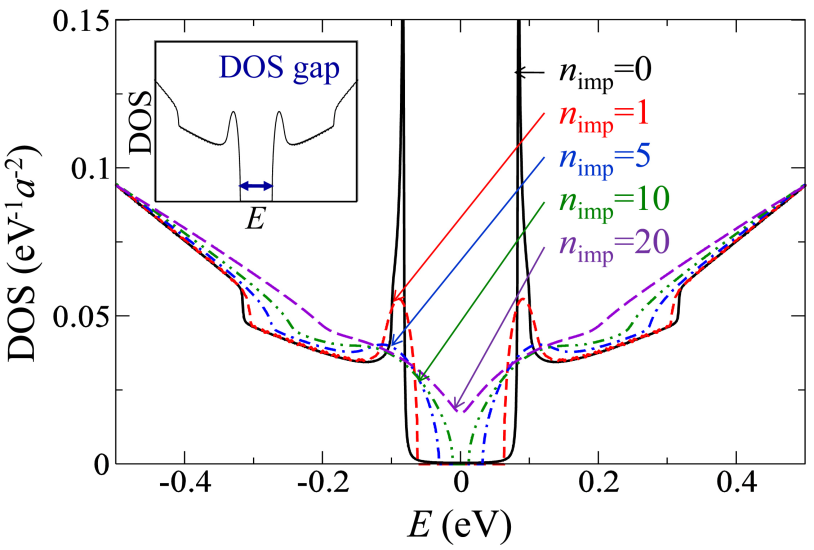
We can now describe the transport and optical gaps within the framework of our theory, defining the gaps as follows. We characterize the gap in the absence of disorder by the associated potential energy difference between the layers in the single particle tight-binding formalism, and label this quantity by . The “sombrero” dispersion of gapped BLG mccann2006 means that the minimum band gap occurs slightly away from the K point such that the bare band gap is . The DOS gap is a theoretical quantity defined as the energy difference between the valence and conduction bands as defined by the onset of the DOS in the SCBA calculation (see the inset to Fig. 1), while the transport gap is extracted from experiments. We note that, due to the possible existence of mid-gap impurity states as well as puddle formation rossi2011 , the transport gap may be lower than the DOS gap. To the best of our knowledge, no evidence of strong localization has so far been seen in transport experiments on BLG, and this allows us to assume that the DOS gap is the effective upper bound for the transport gap.
Following the experimental definition mak2009 , the optical gap is defined as the energy at the top of the first peak in the optical conductivity of intrinsic graphene. This peak results from the direct optical excitations from the valence to the conduction band and is the most direct way of extracting the gap from an optical experiment. This gap is illustrated in the inset to Fig. 3(b).
The effect of disorder on the DOS gap is easy to understand in Fig. 1. With increasing impurity concentration, the gap size reduces and eventually closes at a finite value of the impurity concentration. This figure shows the DOS for a fairly large potential asymmetry eV (which gives eV), and a smaller gap generated by a smaller asymmetry would be closed by a smaller concentration of charged impurities.
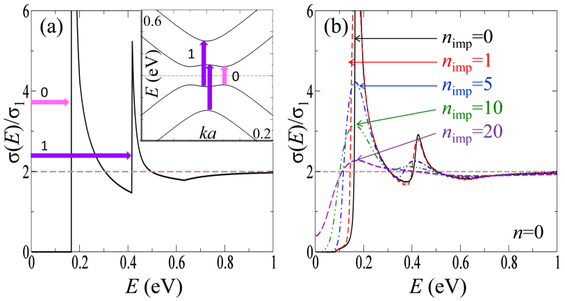
The effect of disorder on the optical gap is also easy to determine if it is extracted from the optical conductivity of intrinsic BLG. Figure 2(a) shows the interband contribution to the nondisordered optical conductivity of intrinsic BLG min2009 along with a sketch showing the origin of the two peaks. The transition labeled “0” is the one with the lowest energy and corresponds to the excitation of carriers across the band gap. Figure 2(b) shows the same quantity in the presence of disorder. In addition to including the impurity scattering effects from , we have included a finite phenomenological level-broadening of meV in the numerics which slightly rounds off the peaks in the case. The introduction of charged impurities further broadens the peaks corresponding to the interband transitions but leaves their position almost unchanged. This explains why the optical gap extracted from experiment [which is defined by the peak value of ] is very close to that predicted by tight-binding theory without disorder.
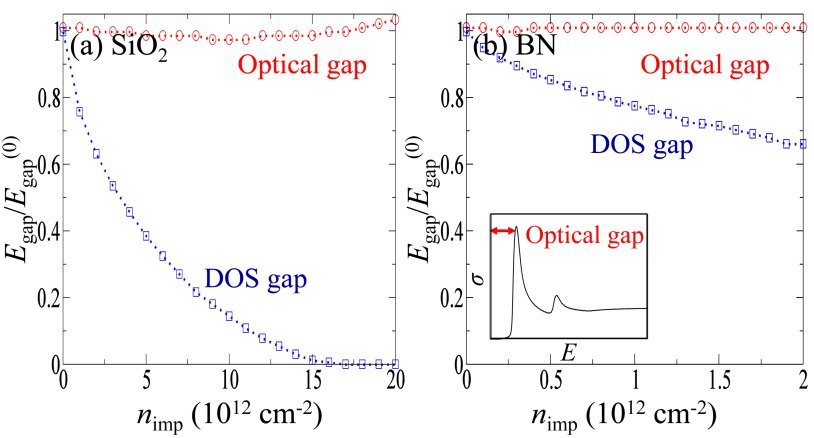
The DOS and optical gaps extracted from these calculations are shown in Fig. 3 as a function of the impurity density substrates . The gaps are identical in the nondisordered system, but as the density of charged impurities increases, the DOS gap is suppressed much more quickly than the optical gap. In the majority of the original experiments on transport in BLG, the samples are made with exfoliated graphene on SiO2 substrates and would therefore have had a large amount of charged impurity disorder. We believe that this observation accounts for the difference in the measured optical and transport gaps in this system. The actual transport gap could be considerably smaller than our theoretical DOS gap rossi2011 , as we have already noted.
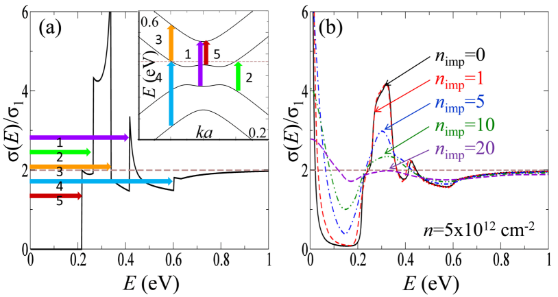
Figure 4 shows the optical conductivity calculated for extrinsic BLG on an SiO2 substrate substrates . In this case, the extra transitions [which are sketched in the inset to Fig. 4(a)] make the optical conductivity a highly nontrivial function of energy and no simple way of extracting an effective optical gap seems obvious. The interband optical conductivity (calculated using the formula from Ref. min2009, ) in the nondisordered case is shown in Fig. 4(a). The inclusion of disorder [Fig 4(b), using Eq. (4)] further masks the structure and makes it very difficult to reliably identify the peaks in the observed optical spectra. The peak at low energy is due to the Drude contribution from intraband processes near the Fermi surface. For example, several experimental studies extract the size of the band gap by comparing the energy of two peaks relating to different interband transitions. In the language of Fig. 4(a), these transitions are labeled 1 (purple online) and 5 (red online). Making the identification with the plot in Fig. 4(b), we see that transition 1 corresponds to the second (smaller) peak, while transition 5 corresponds to the slight shoulder on the low energy side of the main peak. As disorder increases, the peak due to transition 1 quickly disappears, and the shoulder due to transition 5 becomes indistinct. It is therefore impossible to use this method to extract the optical gap in the presence of a realistic amount of charged impurity disorder in BLG, and the peaks seen in the optical conductivity are not obviously related to any individual transition. This is a qualitative new finding of our work.
Finally, we discuss a practical way to test our theory and to bring the DOS and optical gaps much closer in energy. To do this, optical spectroscopy and charge transport experiments should be performed on the same BLG device using an ultra-clean substrate, such as hexagonal boron nitride (h-BN) which has an atomically smooth surface and much lower impurity concentration than current SiO2 devices dean2010 ; dassarma2011 . Recently, gated graphene layers on h-BN substrates have been successfully fabricated dean2010 , and it was demonstrated that graphene on h-BN substrates have substantially higher mobility than graphene on SiO2 substrates by an order of magnitude or more.
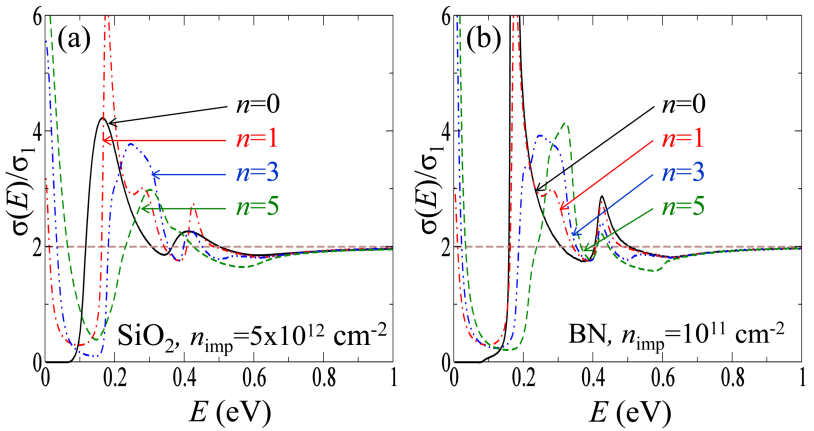
Figures 5(a) and 5(b) show the optical conductivity for a typical impurity density of SiO2 substrate and h-BN substrate for a range of carrier densities. Apart from different disorder strengths, the two substrates are distinguished by different dielectric environments substrates . Because of the relatively low impurity density, the optical conductivity for the h-BN substrate shows sharper peaks than those of SiO2 substrate allowing for more accurate identification of the origin of the various features and hence for a more accurate determination of the band gap. Figure 3(b) shows energy gaps extracted from the DOS and optical conductivity of biased intrinsic BLG with eV on an h-BN substrate as a function of impurity density range. In contrast to the same plots for SiO2 shown in Fig. 3(a), the deviation of the DOS gap from the optical gap for the h-BN substrate is rather small. Note that experimentally realistic values of the impurity density on the h-BN substrate dassarma2011 are of the order of so that the DOS gap is approximately 95% of the optical gap. Therefore, BLG mounted on an h-BN substrate can be used as a tunable gap semiconductor and will yield a significantly higher on/off ratio than the corresponding SiO2 substrate.
In summary, using the SCBA, we have shown that optical experiments and transport measurements do not always probe the same gap in biased BLG. The disorder affects the DOS so that the gap is reduced, while the position of the peak associated with interband transitions in the optical conductivity of intrinsic BLG is rather robust against disorder. In contrast, the features in the optical conductivity of extrinsic BLG which are compared to extract the band gap become indistinct with significant disorder. Our work clearly establishes the danger of extracting a naïve optical band gap in bilayer graphene from the optical absorption data without a thorough theoretical analysis, calling into question several recent experimental claims zhang2009 ; li2009 ; mak2009 . We also suggest that samples with low disorder (such as BLG on an h-BN substrate, or suspended BLG) should show comparable DOS and optical gaps.
The work is supported by US-ONR and NRI-SWAN.
References
- (1) S. Das Sarma, S. Adam, E. H. Hwang. and E. Rossi, Rev. Mod. Phys. 83, 407 (2011).
- (2) A. H. Castro Neto, F. Guinea, N. M. R. Peres, K. S. Novoselov, and A. K. Geim, Rev. Mod. Phys. 81, 109 (2009).
- (3) D. S. L. Abergel, V. Apalkov, J. Berashevich, K. Ziegler, and T. Chakraborty, Adv. Phys. 59, 261 (2010).
- (4) E. McCann, Phys. Rev. B 74, 161403(R) (2006).
- (5) H. Min, B. Sahu, S. K. Banerjee, and A. H. MacDonald, Phys. Rev. B 75, 155115 (2007).
- (6) J. B. Oostinga, H. B. Heersche, X. Liu, A. F. Morpurgo, L. M. K. Vandersypen, Nature Mater. 7, 151 (2007).
- (7) K. Zou and J. Zhu, Phys. Rev. B 82, 081407(R) (2010).
- (8) T. Taychatanapat and P. Jarillo-Herrero, Phys. Rev. Lett. 105, 166601 (2010).
- (9) F. Xia, D. B. Farmer, Y. Lin, and P. Avouris, Nano Lett., 10, 715 (2010).
- (10) S. Xiao, J.-H. Chen, S. Adam, E. D. Williams, and M. S. Fuhrer, Phys. Rev. B 82, 041406 (2010).
- (11) J. Yan and M. S. Fuhrer, Nano Lett., 10, 4521 (2010).
- (12) T. Ohta, A. Bostwick, T. Seyller, K. Horn, and E. Rotenberg, Science 313, 951 (2006).
- (13) Y. Zhang, T.-T. Tang, C. Girit, Z. Hao, M. C. Martin, A. Zettl, M. F. Crommie, Y. Ron Shen, and F. Wang, Nature 459, 820 (2009).
- (14) K. F. Mak, C. H. Lui, J. Shan, and T. F. Heinz, Phys. Rev. Lett. 102, 256405 (2009).
- (15) Z. Q. Li, E. A. Henriksen, Z. Jiang, Z. Hao, M. C. Martin, P. Kim, H. L. Stormer, and D. N. Basov, Phys. Rev. Lett. 102, 037403 (2009).
- (16) F. Wang, Y. Zhang, C. Tian, C. Girit, A. Zettl, M. Crommie, and Y. Ron Shen, Science 320, 206 (2008).
- (17) A. B. Kuzmenko, E. van Heumen, D. van der Marel, P. Lerch, P. Blake, K. S. Novoselov, and A. K. Geim, Phys. Rev. B 79, 115441 (2009).
- (18) S. Adam, E. H. Hwang, V. M. Galitsky, and S. Das Sarma, PNAS 104, 18392 (2007).
- (19) S. Das Sarma, E. Hwang, and E. Rossi, Phys. Rev. B 81, 161407 (2010).
- (20) J. Nilsson and A. H. Castro Neto, Phys. Rev. Lett. 98, 126801 (2007).
- (21) V. V. Mkhitaryan and M. E. Raikh, Phys. Rev. B 78, 195409 (2008).
- (22) N. M. R. Peres, F. Guinea, and A. H. Castro Neto, Phys. Rev. B 73, 125411 (2006).
- (23) T. Stauber, N. M. R. Peres, and A. H. Castro Neto, Phys. Rev. B 78, 085418 (2008).
- (24) T. Ando, J. Phys. Soc. Jpn. 80, 014707 (2011).
- (25) B. Y.-K. Hu, E. H. Hwang, and S. Das Sarma, Phys. Rev. B 78, 165411 (2008).
- (26) F. de Juan, E. H. Hwang, and M. A. H. Vozmediano, Phys. Rev. B 82, 245418 (2010).
- (27) D. S. L. Abergel, H. Min, E. H. Hwang and S. Das Sarma, in preparation.
- (28) G. D. Mahan, Many-Particle Physics (3rd ed.), Kluwer Academic/Plenum Publishers, New York (2000).
- (29) E. Rossi and S. Das Sarma, arXiv:1103.3012 (unpublished).
- (30) H. Min and A. H. MacDonald, Phys. Rev. Lett. 103, 067402 (2009).
- (31) We assume that the bilayer graphene samples have a single gate so that the dielectric environment of the graphene is the average of the gate and air. With and , the effective dielectric constants are and respectively.
- (32) C. R. Dean, A. F. Young, I.Meric, C. Lee, L. Wang, S. Sorgenfrei, K. Watanabe, T. Taniguchi, P. Kim, K. L. Shepard and J. Hone, Nature Nanotech. 5 722, (2010).
- (33) S. Das Sarma and E. H. Hwang, Phys. Rev. B 83, 121405 (2011).