Movable Fiber-Integrated Hybrid Plasmonic Waveguide on Metal Film
Abstract
A waveguide structure consisting of a tapered nanofiber on a metal film is proposed and analyzed to support highly localized hybrid plasmonic modes. The hybrid plasmonic mode can be efficiently excited through the in-line tapered fiber based on adiabatic conversion and collected by the same fiber, which is very convenient in the experiment. Due to the ultrasmall mode area of plasmonic mode, the local electromagnetic field is greatly enhanced in this movable waveguide, which is potential for enhanced coherence light emitter interactions, such as waveguide quantum electrodynamics, single emitter spectrum and nonlinear optics.
Plasmonics in metal nanostructure are being extensively studied for its excellent capability of confining light in subwavelength scale ozbay ; schuller . Since the local electric field of the plasmonic mode is dramatically increased at the dielectric-metal interface, the light-matter interaction can be greatly enhanced. Thus, over the past few years, metal nanostructures including nanoparticles, nanowires and nanorings, have been studied for highly sensitive sensing, surface enhanced Raman scattering, and surface plasmonic amplification by stimulated emission of radiation (SPASER) SPASER ; nie ; sensor ; xiaoprl ; zou2 ; fedutik ; chang1 ; akimov ; dong ; lin . Recently, it has also been found that when an optical emitter (e.g., a quantum dot (QD)) is placed around the silver nanowire, its spontaneous emission can be significantly modified chang1 , known as the Purcell effect. As a result, the plasmonic modes of nanowire provide an alternative approach to study the broadband waveguide quantum electrodynamics (QED) chang1 ; zou2 ; fedutik ; akimov ; dong ; lin , and hold great potential for the single photon source akimov and sub-wavelength single photon transistor chang2 .
One of the limitation of these metal nanostructures is the high absorption loss in metal. Very recently, the hybrid dielectric-metal structures have been proposed, which are consisted of a dielectric waveguide or resonator near a metal substrate. These hybrid plasmonic modes can be low loss while remain high electromagnetic field localization zhang1 ; zhang3 ; xiaoJPB . In experiments, the hybrid plasmonic modes are excited and collected through free space. Unfortunately, this process suffers from low efficiency due to the mismatching of momentum of light. In this paper, we propose and numerically investigate a fiber-integrated hybrid plasmonic waveguide. Based on the adiabatic conversion, the local plasmonic mode can be excited and collected by fiber with very high efficiencies. More importantly, the movable structure can be easily fabricated and controlled, thus offering a great feasibility in future experiment.
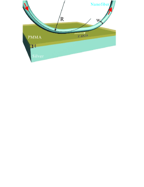
Fig. 1 shows the geometry of the proposed hybrid system. A curved silica nanofiber is put on a silver substrate surrounded by air, with a nano-scale thickness () PMMA polymer film between them PMMA . The curved nanofiber with a sub-micrometer diameter has two symmetrical bending parts (radius ), which are connected by a straight part. In the following study, we fix the working wavelength at nm. The refractive indices of silica and PMMA are and , repectively. In experiment, the nanofiber can be pulled from a standard fiber. The waist of the nanofiber has a uniform diameter (), which can be as small as nm taperexp . The interaction area of the nanofiber and substrate can be selected freely by mounting the nanofiber on a holder system with a high resolution three-axis translation stage.
At the region where the nanofiber contacts with the substrate, the hybrid plasmonic modes will appear zhang1 ; zhang3 ; xiaoJPB . The heart of our proposal is the adiabatic conversion between the fiber guiding mode and the plasmonic mode. As the guiding mode propagates in the bending nanofiber which slowly approaches the metal substrate, the confined field in dielectric will evolute to the plasmonic mode at metal-dielectric interface. Inversely, when the nanofiber slowly deviates from the substrate, the plasmonic mode will convert back to the guiding mode. The similar adiabatic conversion of the optical mode from one mode profile to the other has also been extensively studied in fiber and waveguide optics adiabatic1 ; adiabatic2 . For example, in the slowly varying fiber taper in our structure, the fundamental single-mode fiber mode can be adiabatically converted to the fundamental nanofiber mode with a large evanescent tails extended to the air, with the loss less than . Therefore, the plasmonic mode can be excited and collected efficiently through a standard single-mode fiber.
Now, we analyze the adiabatic process in the present structure. The light propagates along the waveguide, defined as z-axis. Similar to the time evolution of quantum states in Schrodinger function, the evolution of light in waveguides can be expressed as adiabatic1 ; adiabatic2
| (1) |
where is position (z) dependent Hamiltonian due to the variation of waveguide-substrate space, and is the wavefunction at the cross section. At any position of the hybrid waveguide, there exist instantaneous nondegenerate eigenstates of . In the basis of eigenmodes , the electromagnetic field can be expanded as
| (2) |
where is the propagation constant of mode , and is the corresponding coefficient. Substituting Eq.(1) and Eq.(2) into the expression , we can obtain
| (3) |
where . By solving the equation , we obtain
| (4) |
when . Therefore, we can finally obtain
| (5) | |||||
The evolution of states in the hybrid waveguide at the bending region can be obtained by solving the array of equations for all . The first term of Eq.(5) stands for the Berry phase, which does not play a significant role here since we just concern about the energy conversion. The second term represents the coupling between eigenmodes, which reveals the requirement for efficiently adiabatic mode conversion, i.e. . Since the variance of depends on the air space () between waveguide and substrate, we can rewrite as where . When nanofiber approaches the substrate (), . Therefore, the adiabatic conversion requires . In addition, the nanofiber should work in the single mode regime to exclude high order modes, with the single mode criterion .
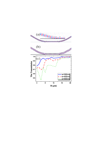
In order to verify the losslessly conversion of the energy between fundamental modes under reasonable parameters, we numerically solve the stationary harmonic propagation of optical field in the nanofiber contacting with silver by two-dimensional finite element method. Due to the complex boundary condition in our structure, we can not analytically solve it by the coupled-mode equation Eq.(5). Figs. 2(a) and 2(b) shows the field distribution as light propagating in the hybrid waveguide. For , the fundamental dielectric modes are almost totally converted to plasmonic mode, as shown in the inset of Fig. 2(a). However, for , we can find that the mode is not totally converted to the plasmonic mode, and the mode in the contact region and transmitted light is multimode. The metal loss is neglected here, so the transmission directly indicates the adiabatic conversion efficiency. Fig. 2(c) shows the transmission of the hybrid waveguide structure, where the waveguide mode converts to the plasmonic mode and then converts back. Clearly, when the radius is larger, the conversion efficiency is higher. When is small, the dynamics is complex, since the adiabatic condition is not fulfilled. For different nanofiber diameter (Fig. 1(c)), thin fiber shows better preformation. The dependence of transmission on and is agree with our theoretical analysis of adiabatic conversion.
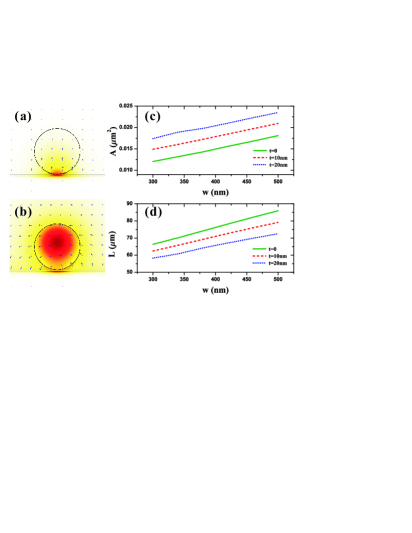
As the lossless adiabatic conversion is confirmed, we turn to analyze the properties of the hybrid plasmonic mode. For reasonable parameters, with m, and nm, the conversion efficiency is about . In the contact region, the cross section is uniform along z-axis, and the hybrid plasmonic mode propagates harmonically along the waveguide. We can investigate the energy distribution at the two-dimensional cross sectionzou , as shown in Figs. 3(a) and 3(b). For the transverse electric (TE) polarization, the energy is localized at the nanofiber-substrate interface, while the transverse magnetic (TM) mode is well confined in the nanofiber. It is evident that the mode area of TE mode is greatly reduced, and the maximum of the electric field is located around nanofiber-substrate interface. We plot the mode area () and propagation length () AL against the waveguide width () for different in Figs. 3(c) and 3(d).
Due to the one-dimensional waveguide confinement, the density of states changes near the nanofiber. As a result, the spontaneous emission rate is modified, which is known as Purcell effect. The maximum emission enhancement can be expressed as xiao
| (6) |
For nanofiber with , and , we get the enhancement of spontaneous emission rate are for a emitter in air and for emitter embed in PMMA. The corresponding collection efficiency of the single emitter fluorescence is in air and in PMMA. Combining with high efficiency adiabatic conversion, we can finally obtain a high collection efficiency directly by fiber.
By a 3D translation stage, this hybrid waveguide can be manipulated or moved easily. Benefiting from the greatly enhanced light-matter interaction, this hybrid plasmonic waveguide structure is potential for experimental realization of the single photon transistors chang2 ; shen or phase flip gate for quantum information science. It should be noted that the enhancement of light emitter interaction is broadband, permitting efficient interaction with quantum dots which have broad emission spectra. For single emitters disperse on the substrate, this hybrid structure can also be use for single photon source or spectrum analyze kartik . Further improvement on this structure to enhance the emitter-light interaction can be done by introducing the bragg-grating mirrors on the nanofiber hakuta .
In conclusion, we have proposed and numerically studied the adiabatic conversion of energy between a dielectric nanofiber and a nanofiber-metal film hybrid plasmonic waveguide structure. The conversion efficiency can exceed , and the movable structure is convenient to be realized in experiment. The hybrid plasmonic mode has very small mode area and low optical loss, permitting strong coherence light-matter interaction, which is potential for studying broadband waveguide QED, single emitter spectrum with high collection efficiency, and nonlinear optics.
The work was supported by the National Fundamental Research Program of China under Grant No. 2011CB921200, the Knowledge Innovation Project of Chinese Academy of Sciences, National Natural Science Foundation of China under Grant No.11004184 and No.10904137.
References
- (1) E. Ozbay, Science 311, 189 (2006).
- (2) J. A. Schuller et al., Nature Materials 9, 193-204 (2010).
- (3) J. M. Bingham et al., J. Am. Chem. Soc. 132, 17358 (2010).
- (4) Y.-F. Xiao et al., Phys. Rev. Lett. 105, 153902 (2010).
- (5) S. Nie et al., Science 275 1102 (1997).
- (6) M. A. Noginov et al., Nature 460,1110 (2009)
- (7) D. E. Chang et al., Phys. Rev. Lett. 97, 053002 (2006).
- (8) Y. Fedutik et al., Phys. Rev. Lett. 99, 136802(2007).
- (9) A. V. Akimov et al., Nature 450, 402 (2007).
- (10) C.-L. Zou et al., J. Opt. Soc. Am. B 27, 2495(2010).
- (11) C.-H. Dong et al., Appl. Phys. Lett. 95, 221009(2009).
- (12) Z.-R. Lin et al., Phy. Rev. B 82, 241401(R) (2010).
- (13) D. E. Chang et al., Nature Phys. 3, 807 (2007).
- (14) R. F. Oulton et al., Nature Photon. 2, 496 (2008).
- (15) R. F. Oulton et al., Nature 461, 629 (2009).
- (16) Y.-F. Xiao et al., J. Phys. B 43, 035402 (2010).
- (17) In experiments, emitters can be dispersed into PMMA and fixed by the nanofilm.
- (18) A. Stiebeiner et al., Opt. Express 18, 22677 (2010).
- (19) M. Skorobogatiy et al., Opt. Express 10, 1227 (2002).
- (20) S. G. Johnson et al., Phys. Rev. E 66, 066608 (2002).
- (21) C.-L. Zou et al., Appl. Phys. Lett. 97, 183102 (2010).
- (22) The defination of A and L can be found in ref.zou .
- (23) Y.-F. Xiao et al., arXiv: 1010.5067.
- (24) J. T. Shen, and S. Fan, Opt. Lett. 30, 15 (2005).
- (25) M. I. Davanco and K. Srinivasan, Opt. Lett. 34, 2542 (2009).
- (26) F. L. Kien and K. Hakuta, Phys. Rev. A 81, 023812 (2010).