Ionization wave propagation on a micro cavity plasma array
Abstract
Microcavity plasma arrays of inverse pyramidal cavities have been fabricated in p-Si wafers. Each cavity acts as a microscopic dielectric barrier discharge. Operated at atmospheric pressure in argon and excited with high voltage at about 10 kHz, each cavity develops a localized microplasma. Experiments have shown a strong interaction of individual cavities, leading to the propagation of wave-like optical emission structures along the surface of the array. This phenomenon is numerically investigated using computer simulation. The observed ionization wave propagates with a speed of about 5 km/s, which agrees well the experimental findings. It is found that the wave propagation is due to sequential contributions of a drift of electrons followed by drift of ions between cavities seeded by photoemission of electrons by the plasma in adjacent cavities.
Atmospheric pressure microplasmas have gained increasing attention since the early work on microhollow cathode discharges by Schoenbach et al. Schoenbach1996 . Although they are highly collisional, microplasmas show strong non-equilibrium behavior Penache2002 . Electrons are hot (up to a few eV) while ions and and the neutral gas are cold (about room temperature in most cases, though temperatures of many hundreds Centigrade occur at high power loading). Microplasmas are characterized by high electron densities (up to a few cm-3) and high power densities (up to some 100 kW/cm3). Due to these unique properties microplasmas have found widespread use in technological and biomedical applications Becker2006 ; Morfill2009 ; Becker2010 ; Lee2011 , such as surface treatment, sterilization, and lighting. At the same time microplasmas continue to show unexpected phenomena and are therefore scientifically interesting. For example, arrays of microplasmas having thousands of individual microdischarges have been fabricated as efficient lighting sources Eden2005 . When excited by AC voltages, the initiation of optical emission from such arrays has shown wave-like phenomena, propagating across the array at speeds of a few kilometers per second. In this paper, we discuss results from experimental and computational investigations of these wave-like propagation of optical emission.
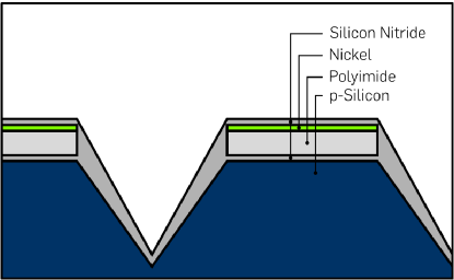
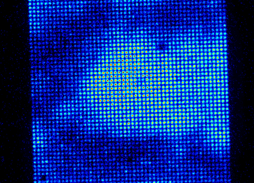
The microcavity array we investigated, developed by Eden et al. Eden2005 , has individual inverse pyramidal cavities fabricated on p-Si wafers (see Fig. 1), combined with a nickel grid as a counter electrode and dielectric coatings. Each cavity – in essence a microscopic dielectric barrier discharge (DBD) – has a base opening of 50 50 m and a depth of 35 m. The separation of the individual cavities is 50 m. The entire array consists of 50 by 50 microplasmas. When operated with a sawtooth voltage of about 10 kHz in atmospheric pressure argon, the array emits a bright glow in the visible wavelength range, which visually appears homogeneous over the entire array. However, spatially and temporally resolved emission spectroscopy shows that wave-like structures (see Fig. 2) propagate across the array, indicating that the individual microdischarges strongly interact with each other Waskoenig2008 ; Boettner2010 .
The related computer simulation was performed using the modeling platform nonPDPSIM, described in detail in Kushner2004 ; Babaeva2007 ; Babaeva2009 . Here we briefly discuss the relevant physical equations. Poisson’s equation for the electrostatic potential is self-consistently coupled with drift-diffusion equations for the charged species and the surface charge balance equation. The set of equations is simultaneously integrated in time using an implicit Newton iteration technique. This integration step is followed by an implicit update of the electron temperature by solving the electron energy equation. To capture the non-Maxwellian behavior of the electrons, the electron transport coefficients and rate coefficients are obtained by solving the zero-dimensional Boltzmann’s equation for the electron energy distribution. A Monte Carlo simulation is used to track the trajectories of sheath accelerated secondary electrons. The transport of photons is treated by means Green’s function method. The discharge is sustained in argon at atmospheric pressure. The species in the model are electrons, Ar(3s), Ar(4s), Ar(4p), Ar+, Ar and Ar. The photon transport we tracked in the model is emission dimmer radiation Ar. In the absence of impurities and large densities of excited states, this emission is optically thin. The reaction mechanism is summarized in Ref. Bhoj2004a .
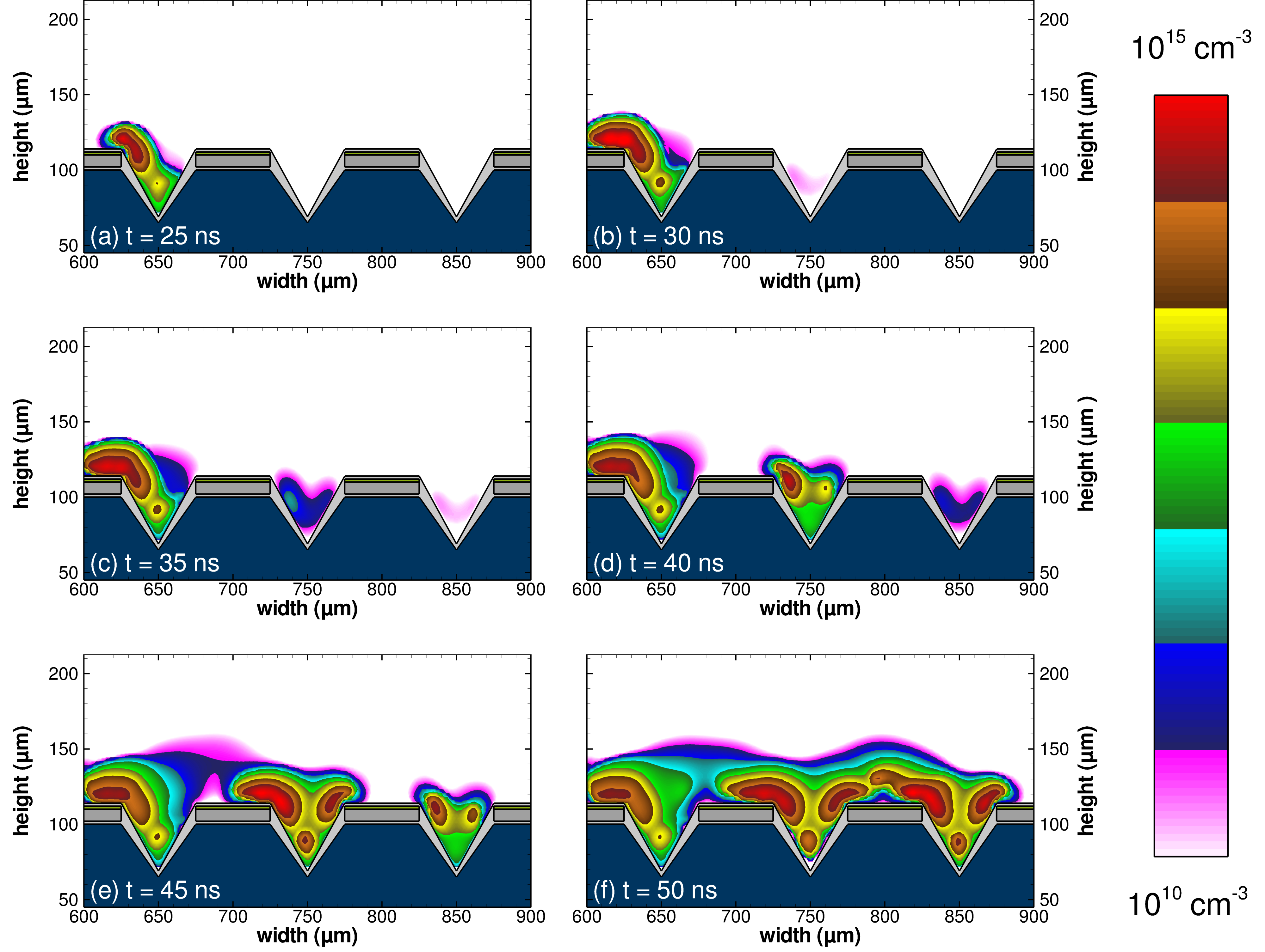
The simulation addresses a sub-system of the micro cavity array over a time interval of 50 ns. The geometry is two-dimensional and consists of three neighboring cavities, which appear in the model as slits. The entire computational domain is 1 mm tall by 1.5 mm wide, with boundaries of which are electrically grounded. The conductivity of the wafer in contact with the boundary is 0.17 cm. The secondary electron emission coefficient by ions is 0.15 on all surfaces. A photoelectron emission coefficient of 0.05 is assumed on the dielectric surface. The step function DC potential of V is applied to the embedded nickel electrode grid.
The initial plasma density is a Gaussian shaped spot of plasma 10 m wide and cm-3 in magnitude at the left vertex of the left cavity. The resulting electron density as a function of time is shown in Fig. 3. Ions accelerated by the negative potential of the nickel grid drift towards the vertex of the cavity and initiate secondary electron emission. The secondary electrons are accelerated into the cavity and generate ions and electrons. The ionization rate peaks at the vertices at about cm-3 s-1 with an electron temperature of 8 eV, and then spreads on the top dielectric, similar to a conventional DBD. Meanwhile, photons produced by relaxation of Ar lead to photoelectron emission on the dielectric surfaces, mainly at the right vertex of the neighboring cavity. At ns a sufficiently large electron density of about cm-3 is reached in the left cavity, that the potential is shielded from the interior of the left cavity and the discharge turns from a Townsend mode to a glow mode. The quasineutral region fills the left cavity and spreads over its edges, charging the top dielectric. 5 ns after the left cavity is ignited, an electron density larger than cm-3 is produced in the middle cavity initiated by avalanching of photo-generated electrons, and another 5 ns later in the right cavity. Both cavities undergo a transition from a Townsend mode to glow mode 10 ns after the initial electron density is generated (Fig. 3d,e). In all three cavities a quasineutral region develops. These individual plasmas connect after their expansion out of the cavities, as shown in Fig. 3f. The electron density peaks in the head of the avalanche with cm-3. Within the cavities the electron density exceeds cm-3 leading to a Debye length m. During the ignition, the electron temperature reaches 5 eV within the cavities, but decays rapidly. The observed densities agree with values expected for this kind of discharge Becker2006 .
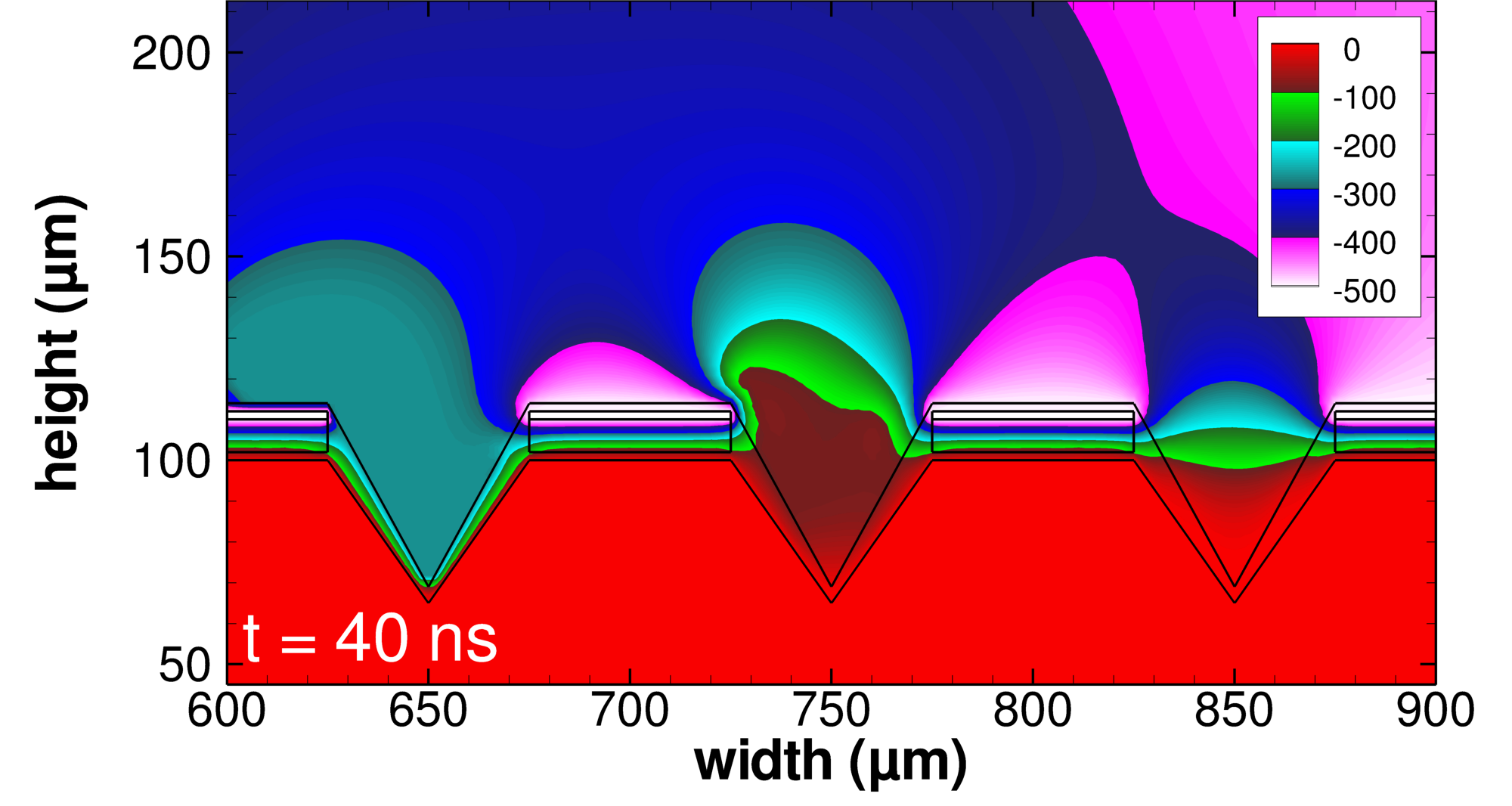
The electric potential is plotted at ns in Fig. 4. It shows the three phases of the discharge development. The potential in the right cavity is essentially the vacuum potential – there is little space charge to influence the electrical field. The left cavity in contrast contains a quasineutral plasma with the plasma being nearly equipotential. The majority of the potential is dropped over the dielectrics which covers the anode and the cathode, as one expects for a dielectric barrier discharge. The electron avalanche within the center cavity produces an equipotential channel which merges with that of the left cavity and indicates the transition from a Townsend mode to a glow mode discharge.
Taking the time between the ignition of the left and the right cavity one finds an effective ionization propagation speed of about 5 km/s which agrees very well with the measured propagation speed of 5 to 10 km/s. In the absence of photoelectron emission, the propagation speed is about 1 km/s. Although not all effects are addressed with our simulation, the ionization wave is well described. Other effects of importance are surface charges accumulated in a previous half cycle and a second ionization wave after an further increase of the voltage. The effect of surface charges accumulated at a previous half cycle with an inverse voltage results in an enhancement of the electrical field an reduces the breakdown voltage. Both are a matter of ongoing research. To summarize, the observed ionization wave is driven by photoelectrons emitted at neighbored cavities. These electron source causes the ignition of a single cavity and provides new photons to sustain the ionization wave propagation.
The authors gratefully acknowledge financial support by the Deutsche Forschungsgemeinschaft in the frame of Research Group 1123 Physics of Microplasmas as well as the Ruhr University Research School.
References
- (1) K.H. Schoenbach, R. Verhappen, T. Tessnow, F.E. Peterkin, W.W. Byszewski, Appl. Phys. Lett. 68, 13 (1996)
- (2) C. Penache, M. Miclea, A. Bräuning-Demian, O. Hohn, S. Schössler, T. Jahnke, K. Niemax, and K. Schmidt-Böcking, Plasma Sources Sci. Technol. 11, 476 (2002)
- (3) K.H. Becker, K.H. Schoenbach, and J.G. Eden, J. Phys. D: Appl. Phys. 39, R55 (2006)
- (4) M.G. Kong, G. Kroesen, G.E. Morfill, T. Nosenko, T. Shimizu, J. van Dijk, J.L. Zimmermann, New. J. Phys. 11, 115012 (2009)
- (5) K.H. Becker, H. Kersten, J. Hopwood, J.L. Lopez, Eur. Phys. J. D 60, 437 (2010)
- (6) H.W. Lee, G.Y. Park, Y.S. Seo, Y.H. Im, S.B. Shim, and H.J. Lee, J. Phys. D: Appl. Phys 44, 053001 (2011)
- (7) J.G. Eden, S.-J. Park, N.P. Ostrom, K.-F. Chen, J. Phys. D: Appl. Phys. 38 1644 (2005)
- (8) J. Waskoenig, D. O’Connell, V. Schulz-von der Gathen, J. Winter, S.-J. Park and J.G. Eden, Appl. Phys. Lett. 92, 101503 (2008)
- (9) H. Boettner, J. Waskoenig, D. O’Connell, T.L. Kim, P.A. Tchertchian, J. Winter, and V. Schulz-von der Gathen, J. Phys. D: Appl. Phys. 43 124010 (2010)
- (10) M.J. Kushner, J. Appl. Phys. 95, 846 (2004)
- (11) N.Y. Babaeva, R. Arakoni, and M.J. Kushner, J. Appl. Phys. 101, 123306 (2007)
- (12) N.Y. Babaeva, and M.J. Kushner, Plasma Sources Sci. Technol., 18 035009 (2009)
- (13) A.N. Bhoj, and M.J. Kushner, J. Phys. D: Appl. Phys. 37, 2510-26 (2004)