Second harmonic generation in GaP photonic crystal waveguides
Abstract
We demonstrate enhanced second harmonic generation in a gallium phosphide photonic crystal waveguide with a measured external conversion efficiency of 510-7/W. Our results are promising for frequency conversion of on-chip integrated emitters having broad spectra or large inhomogeneous broadening, as well as for frequency conversion of ultrashort pulses.
Nonlinear frequency conversion processes can be strongly enhanced in semiconductor photonic nanocavities and waveguidesCorcoran et al. (2009); Rodriguez et al. (2007); Bravo-Abad et al. (2010); Burgess et al. (2009); Liscidini and Andreani (2004), dramatically reducing the required physical footprint and providing an integrated, on-chip platform. Such devices are useful as on-chip light sources at otherwise inaccessible wavelengths, as well as for interfacing between multiple quantum emitters with different frequencies or between quantum emitters and telecommunications wavelengthsMcCutcheon et al. (2009); Rivoire et al. (2011).
Previous work in nanophotonic nonlinear frequency conversionMcCutcheon et al. (2007); Rivoire et al. (2009a); Rivoire et al. (2010) has focused on using nanophotonic cavities with high quality factor (Q) to generate a resonant enhancement in conversion efficiency at the wavelength of the cavity mode; however, the bandwidth allowed by a high-Q cavity would be unsuitable for frequency conversion of quantum emitters with a broadband spectrum (such as the nitrogen vacancy (NV) center) or frequency conversion of ultrashort pulses. Photonic crystal waveguides offer an alternative to cavities; the waveguide photonic dispersion can produce large slow-down factors greatly increasing the effective nonlinear interaction length over a broad wavelength rangeCorcoran et al. (2009, 2010). Third harmonic frequency conversion has been previously demonstrated in a silicon photonic crystal waveguideCorcoran et al. (2009); however, the efficiency is limited by the weak nonlinearity of the material, linear absorption of the third harmonic, and two-photon absorption of the fundamental frequency. Here, we demonstrate second harmonic generation using the nonlinearity of gallium phosphide, which has a large electronic band gap (550 nm) minimizing absorption. The circulating intensity in the waveguide is enhanced by the group index , providing a factor of enhancement in conversion efficiency compared to a conventional waveguide with similar size. This material is compatible with quantum emitters including InPHatami et al. (2003) and InGaAs quantum dotsSong et al. (2010), NV centersEnglund et al. (2010), and fluorescent moleculesRivoire et al. (2009b).
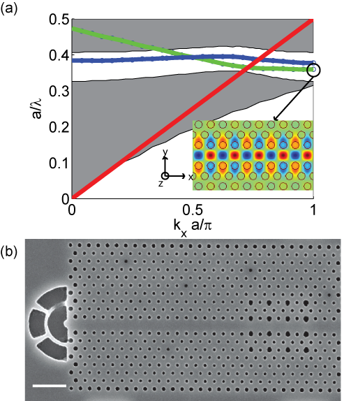
Fig. 1 shows the dispersion diagram of transverse electric (TE)-like modes of the W1 waveguide (in-plane E field component only at the center of the slab). The W1 waveguide is formed by removing one row of holes from the triangular latticeLončar et al. (2009). The photonic band gap is indicated by the white region between the shaded gray areas. The structure supports two guided modes inside the band gap with even (mode of interest) and odd symmetry of the field component relative to the -plane containing the waveguide axis. The inset shows the field component of the photonic crystal waveguide mode calculated from 3D finite difference time domain (FDTD) simulation at the = point for the green band (even mirror symmetry). Here, no other changes to the photonic crystal have been made, although group velocity dispersion could be minimized using modified designs shifting the first two rows of holes relative to the defectLi et al. (2008).
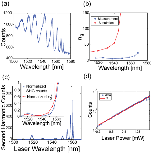
Fig. 1b shows a scanning electron microscope (SEM) image of a photonic crystal waveguide, fabricated in a 164 nm thick gallium phosphide membrane. The membrane is grown by gas-source molecular beam epitaxy on top of a 1 m thick layer of Al0.85Ga0.15P on a (100)-oriented gallium phosphide wafer. The structures are fabricated by e-beam lithography and dry etching through the GaP membrane followed by a wet etch to remove the sacrificial layer yielding a suspended membrane. The W1 waveguide is fabricated with lattice constant =560 nm, hole radius 0.25, and is 30 periods (17 m) long. To access wavevectors of the dispersion lying below the light line (which have low loss and large group index) from normal incidence, the structure includes two grating couplers: a circular grating on the leftFaraon et al. (2008) and a coupler on the right formed by perturbing the lattice with periodicity using enlarged holesEnglund et al. (2009) (used only for transmission measurements). The structures are oriented with the waveguide along a [011] crystal direction. For transmission measurements, an objective lens with numerical aperture of 0.5 is positioned above right grating; the light source is focused slightly off-center onto the left grating. Fig. 2a shows transmission measurements using a tungsten halogen white light source. Periodic peaks in transmission result from the finite length of the waveguide (30 periods) which supports Fabry Perot (FP)-like reflections with peaks separated by where is the length of the waveguide and is the group indexNotomi et al. (2001). The linewidths of the peaks becomes narrower as the wavelength increases entering the part of the dispersion below the light line. The derived group index is shown in Fig. 2b. The maximum group index measured is 25, lower than expected from simulation (Fig. 2)b, but still much larger than in a conventional waveguide.
To measure second harmonic generation, we couple light from a tunable continuous wave telecommunications-wavelength laser (Agilent 81989A) into the left grating. Second harmonic generated inside the waveguide scatters out of plane and is collected by the same objective placed above the center of the structure from the entire field of view onto a camera for imaging or a monochromator and CCD for spectral analysis. The collected second harmonic radiation as a function of incident laser wavelength is shown in Fig. 2c for a different structure with slightly larger that better matched the range of our tunable laser. Conversion is observed over a range of incident wavelengths, with periodic peaks again observed from FP reflections at the fundamental wavelength. The inset shows the close match between the second harmonic counts at the FP peaks and the expected enhancement, where is calculated from the spacing between FP peaks in the second harmonic data. Fig. 2d shows the second harmonic counts measured as a function of incident laser transmitted through the objective. The laser wavelength is 1561.5 nm; the calculated group index for this structure at this wavelength is 30. A log-log fit of the data yields a slope of 1.9, close to what is expected for a second-order process. The estimated external conversion efficiency, calculated from the maximum second harmonic intensity is 10-9 for 2 mW transmitted through the objective, or 510-7/W. The power at second harmonic wavelength was measured by separately calibrating the spectrometer counts with a laser at the second harmonic wavelength using a power meter. This is four orders of magnitude less than measured for photonic crystal cavities in GaPRivoire et al. (2009a). As a comparison to previous work on frequency conversion in III-V semiconductors, we note that our device has only times lower second harmonic external conversion efficiency for 1.5 m light, although it has not been optimized for incoupling or outcoupling efficiency and has a waveguide length 300 times shorter than past experiments (using GaAs/AlGaAs waveguides phase matched by orientation patterningYu et al. (2005) that require significantly more complicated MBE growth).
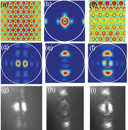
Because the only nonzero elements of the tensor for (100)-grown GaP have and the guided mode of the photonic crystal waveguide at the fundamental wavelength has electric field in-plane only, the second harmonic must have electric field out-of-plane, e.g. couple to transverse magnetic-like (TM-like) mode. A 3D FDTD simulation of electric field at the second harmonic frequency in a periodic triangular photonic crystal lattice is shown in Fig. 3a; the symmetry of the electric fields indicates a monopole mode with far-field radiation pattern (calculated through Fourier transform of the field immediately above the slabVučković et al. (2002)) shown in Fig. 3b. The removal of a row of holes to form the W1 photonic crystal waveguide perturbs this mode; the resulting electric field is shown in Fig. 3c, with far field patterns in Figs. 3d-f. The simulated quality factor of the mode is 200, more than an order of magnitude lower than for the same mode unperturbed by the waveguide. To verify experimentally that we collect second harmonic through this mode, we image the radiation pattern from the waveguide onto a camera (Figs. 3g-i) using a Glan Thompson polarizer to resolve different polarizations; the resulting images show very good agreement with the simulations. The wavelength of the incident laser for these measurements is 1561.5 nm (, in good agreement with simulations (Fig. 1)).
In conclusion, we demonstrate enhancement of second harmonic generation in GaP in a photonic crystal waveguide with maximum group index of 30. We measure an external conversion efficiency of 510-7/W or 10-9 for 2 mW incident power. The large electronic band gap of GaP minimizes linear absorption of the second harmonic as well as two-photon absorption of the fundamental. Our results are promising for frequency conversion of on-chip integrated emitters having broad spectra (e.g., NV centers) or large inhomogeneous broadening (e.g., InAs/GaAs quantum dots), as well as for frequency conversion of ultrashort pulses.
Financial support was provided by the National Science Foundation (NSF Grant ECCS-10 25811 ). KR and SB supported by Stanford Graduate Fellowships and the NSF GRFP (SB). This work was performed in part at the Stanford Nanofabrication Facility of NNIN supported by the National Science Foundation under Grant No. ECS-9731293.
References
- Corcoran et al. (2009) B. Corcoran, C. Monat, C. Grillet, D. Moss, B. Eggleton, T. White, L. O’Faolain, and T. Krauss, Nature Photon. 3, 206 (2009).
- Corcoran et al. (2010) B. Corcoran, C. Monat, M. Pelusi, C. Grillet, T. White, L. O’Faolain, T. Krauss, B. Eggleton, and D. Moss, Opt. Express 18, 7770 (2010).
- Rodriguez et al. (2007) A. Rodriguez, M. Soljacic, J. D. Joannopoulos, and S. G. Johnson, Opt. Express 15, 7303 (2007).
- Bravo-Abad et al. (2010) J. Bravo-Abad, A. Rodriguez, J. Joannopoulos, P. Rakich, S. Johnson, and M. Soljačić, Appl. Phys. Lett. 96, 101110 (2010).
- Burgess et al. (2009) I. B. Burgess, Y. Zhang, M. W. McCutcheon, A. W. Rodriguez, J. Bravo-Abad, S. G. Johnson, and M. Loncar, Opt. Express 17, 20099 (2009).
- Liscidini and Andreani (2004) M. Liscidini and L. C. Andreani, Appl. Phys. Lett. 85, 1883 (2004).
- McCutcheon et al. (2009) M. W. McCutcheon, D. E. Chang, Y. Zhang, M. D. Lukin, and M. Loncar, Opt. Express 17, 22689 (2009).
- Rivoire et al. (2011) K. Rivoire, S. Buckley, A. Majumdar, H. Kim, P. Petroff, and J. Vučković, Appl. Phys. Lett. 98, 083105 (2011).
- McCutcheon et al. (2007) M. W. McCutcheon, J. F. Young, G. W. Rieger, D. Dalacu, S. Frédérick, P. J. Poole, and R. L. Williams, Phys. Rev. B 76, 245104 (2007).
- Rivoire et al. (2009a) K. Rivoire, Z. Lin, F. Hatami, W. T. Masselink, and J. Vučković, Opt. Express 17, 22609 (2009a).
- Rivoire et al. (2010) K. Rivoire, Z. Lin, F. Hatami, and J. Vučković, Appl. Phys. Lett. 97, 043103 (2010).
- Hatami et al. (2003) F. Hatami, W. T. Masselink, L. Schrottke, J. W. Tomm, V. Talalaev, C. Kristukat, and A. R. Goñi, Phys. Rev. B 67, 085306 (2003).
- Song et al. (2010) Y. Song, P. Simmonds, and M. Lee, Appl. Phys. Lett. 97, 223110 (2010).
- Englund et al. (2010) D. Englund, B. Shields, K. Rivoire, F. Hatami, J. Vučković, H. Park, and M. Lukin, Nano Lett. 10, 3922 (2010).
- Rivoire et al. (2009b) K. Rivoire, A. Kinkhabwala, F. Hatami, W. Masselink, Y. Avlasevich, K. Muellen, W. Moerner, J. Vučković, H. Park, and M. Lukin, Appl. Phys. Lett. 95, 123113 (2009b).
- Lončar et al. (2009) M. Lončar, T. Doll, J. Vučković, and A. Scherer, J. Lightwave Tech. 18, 1402 (2009).
- Li et al. (2008) J. Li, T. P. White, L. O’Faolain, A. Gomez-Iglesias, and T. F. Krauss, Opt. Express 16, 6227 (2008), URL http://www.opticsexpress.org/abstract.cfm?URI=oe-16-9-6227.
- Faraon et al. (2008) A. Faraon, I. Fushman, D. Englund, N. Stoltz, P. Petroff, and J. Vuckovic, Opt. Express 16, 12154 (2008).
- Englund et al. (2009) D. Englund, B. Ellis, E. Edwards, T. Sarmiento, J. S. Harris, D. A. B. Miller, and J. Vuckovic, Opt. Express 17, 15409 (2009).
- Notomi et al. (2001) M. Notomi, K. Yamada, A. Shinya, J. Takahashi, C. Takahashi, and I. Yokohama, Phys. Rev. Lett. 87, 253902 (2001).
- Yu et al. (2005) X. Yu, L. Scaccabarozzi, J. J. S. Harris, P. S. Kuo, and M. M. Fejer, Opt. Express 13, 10742 (2005), URL http://www.opticsexpress.org/abstract.cfm?URI=oe-13-26-10742.
- Vučković et al. (2002) J. Vučković, M. Lončar, H. Mabuchi, and A. Scherer, IEEE J. Quant. Electron. 38, 850 (2002).