Transport Properties of Clean Quantum Point Contacts
Abstract
Quantum point contacts are fundamental building blocks for mesoscopic transport experiments and play an important role in recent interference- and fractional quantum Hall experiments. However, it is not clear how electron-electron interactions and the random disorder potential influence the confinement potential and give rise to phenomena like the mysterious 0.7 anomaly. Novel growth techniques of heterostructures for high-mobility two-dimensional electron gases enable us to investigate quantum point contacts with a strongly suppressed disorder potential. These clean quantum point contacts indeed show transport features that are obscured by disorder in standard samples. From this transport data, we are able to extract the parameters of the confinement potential which describe its shape in longitudinal and transverse direction. Knowing the shape (and hence the slope) of the confinement potential might be crucial to predict which interaction-induced states can form best in quantum point contacts.
pacs:
72.20.-i, 72.25.Dc, 73., 75.76.+j1 Introduction
Quantum devices on semiconductor nanostructures rely on quantum point contacts (QPCs) as basic building blocks. Quantized conductance has been observed early on [1, 2] and it has been used as a signature of the quality of a QPC. With ever improving sample quality and the perspective for the detection of non-abelian anyons in the fractional quantum Hall state, several experiments [3, 4, 5] have recently used the properties of QPCs fabricated on ultra high-mobility two-dimensional electron gases (2DEGs). In view of proposals to investigate fractional quantum Hall states in confined geometries and interferometer-like setups, the detailed understanding and control of QPCs are essential. Here we present experimental data which go beyond previously published data by demonstrating experiments that profit from the extraordinary cleanliness of the high-mobility 2DEG. In contrast to standard 2DEGs, we do not observe defect-induced resonances when the QPCs are shifted laterally. Higher order half plateaus are observed in the finite-bias differential conductance (at magnetic field ) as well as spin-split half plateaus at . Finally, the -anomaly is investigated as a function of temperature and in perpendicular magnetic field.
2 Experiment
The samples are fabricated on a high-mobility wafer with a two-dimensional electron gas (2DEG) residing beneath the surface. The high mobility is achieved by placing Si dopants in a narrow GaAs layer sandwiched by AlAs layers [6, 7, 8]. The population of the band in AlAs results in hardly mobile electrons which screen the static disorder potential but do not cause a measurable parallel conductance. Optical lithography is employed to define Hall bars via mesa etch and deposition of Au/Ge Ohmic contacts. Processed Hall bars have an electron density of and Drude mobilities in the range of . The characterization as well as the following experiments are carried out at a temperature of , if not stated otherwise. Schottky electrodes are defined via electron beam lithography and subsequent deposition of Ti/Au. AFM micrographs of two QPCs are shown in the insets of Figs. 1a) and b).
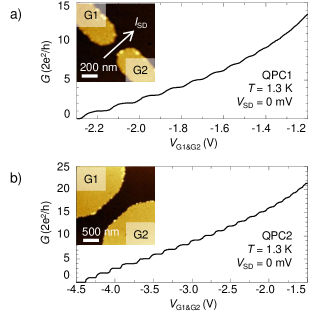
The gates appear bright with the gap between them being (a) and (b). Applying a voltage of to the gates depletes the underlying 2DEG and creates a constriction between source and drain. The source-drain current and the voltage drop across the QPC are measured in four-terminal configuration while applying a small lock in amplitude of at a frequency of to source and drain. A DC source-drain voltage can be added to with both voltages being applied symmetrically with respect to the common reference potential of source, drain and the gates. Most transport properties of the employed high-mobility heterostructures are hysteretic as a function of gate bias [9]. Therefore all traces are recorded in the same sweep direction by sweeping towards more negative values of gate voltage.
Figure 1a) shows the differential conductance () of QPC1, plotted as a function of the voltage applied to gates G1 and G2. From the Fermi wavelength of the 2DEG and the distance of the gates, it would be expected that modes can be observed due to confinement transversal to the electron flow [2]. Indeed, the number of quantized plateaus in Fig. 1a) agrees with this estimation, indicating that the largest electronic width of the QPC matches the lithographic gap of the Schottky split-gates. Due to the larger gate-spacing of QPC2, correspondingly more modes are observed in Fig. 1b) and a significantly larger gate bias has to be applied in order to pinch off. We observe irreversible charging of the sample typically at which limits the QPCs’ range of operation.
2.1 Lateral Shifting of the QPC
QPC1 can be further characterized by varying the voltages applied to each of the gates, which is not possible for QPC2 due to its extreme pinch-off voltage. Figure 2 shows the transconductance of QPC1 in grayscale, plotted as a function of and .
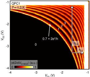
Black areas correspond to pinch-off (bottom left) and successive conductance plateaus (marked by ). Such a plot reveals scattering centers in the channel, since changing the ratio of gate voltages causes the position of the channel to shift laterally between the gates [10]. The shift can be approximately determined by counting the number of steps (, ) that can be observed as a function of each gate [11]: . In the situation marked by white arrows in Fig. 2 this amounts to . The largest observed shift is , which corresponds to the lithographic distance of the gates. When the QPC is shifted from one gate to the other, its potential would naturally change if localized impurities in the channel or the static disorder potential created by the dopants were relevant. Since these defects are fixed in space, they should appear as lines intersecting the QPC steps, with their slope given by the capacitance to gates G1 and G2. The absence of such defect-induced lines confirms the cleanliness of the sample and the effectiveness of the screening layers in suppressing the charged dopants’ disorder potential.
2.2 The 0.7-Anomaly in Perpendicular Magnetic Field
It is noteworthy that the 0.7 anomaly [12, 13, 14], an additional plateau with a conductance of , appears as a weak shoulder close to pinch-off of both QPCs. In the transconductance-plot in Fig. 2, the 0.7 anomaly is visible as an asymmetry of the pinch-off line, giving rise to a gray (red) stripe adjacent to the plateau. The 0.7-stripe is continuous and reaches all the way to the extreme QPC shifts, emphasizing that the 0.7-anomaly is an intrinsic property of the QPC. Cuts along the diagonal (where as well as strongly shifted configurations (either or being fixed at ) are shown in Fig. 3.
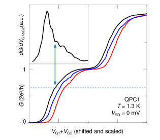
When the QPC is defined centrally in-between the gates (, leftmost trace), the 0.7-anomaly manifests itself as a weak shoulder below the -plateau. The top left inset shows the numerically derived slope which exhibits a clear change of slope at the position marked by an arrow. The corresponding conductance at this gate voltage is . For comparison, two configurations with the QPC being defined close to gate G2 (central trace) or gate G1 (rightmost trace) are plotted on the same gate axis. We find that both asymmetrically measured traces resemble the shape of the symmetric case. The conductance value of the 0.7-anomaly does not change when shifting the QPC laterally, however our accuracy of determining it is limited to due to switching events caused by the more negative gate voltages required for pinch-off in an asymmetric gate configuration. In agreement with previous studies [12, 13, 14], we find that the 0.7-anomaly is less pronounced in 2DEGs with high density (here: ) compared to samples with electron densities in the range of .
In order to compare the results obtained on low-density 2DEGs to the behavior of our system, the temperature- and magnetic-field-dependence is investigated in detail. However, similar to recent work performed on comparable high-mobility 2DEGs [15], we find a suppression of the Hall mobility in parallel magnetic field which is in our devices accompanied by a suppression of the QPCs’ spin splitting (data not shown). We are hence limited to applying a magnetic field perpendicular to the 2DEG, which should also weaken the 0.7-anomaly by lifting the spin degeneracy. Since the differential conductance is strongly modified by the presence of edge channels in the quantum Hall regime, the filling factor is obtained from the diagonal voltage drop across QPC1. Figure 4a) shows the lower part of the pinch-off trace for different temperatures without a magnetic field being applied.
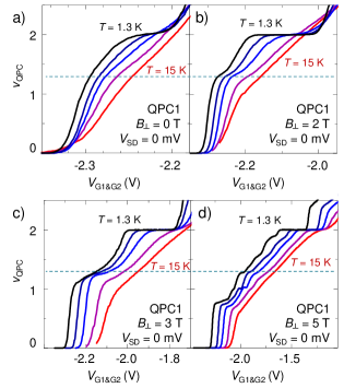
As expected, the 0.7-anomaly evolves into a more pronounced shoulder when the temperature is increased from (left) to (right). The marked value of (dashed line) corresponds to the conductance of extracted from Fig. 3.
By applying a magnetic field perpendicular to the 2DEG, we expect the 0.7-anomaly to be influenced by the increase of both the energetic and spatial separation of the lowest two spin channels. This idea of “mimicking the 0.7 scenario” was previously investigated in [16], but the interpretation of the data proved difficult due to additional resonances in the pinch-off traces. Figure 4b) is recorded at , where spin-resolved edge channels begin to form at . The data shows a well pronounced plateau at which is weakened when the temperature is increased to . Figure 4c) shows the same measurement at , where the edge channels are further separated energetically as well as spatially. Now, the temperature dependence is non-monotonic with the 0.7-anomaly first rising almost to the expected transmission of , then decaying to lower transmission. Data taken at is shown in Fig. 4d). The structure is more complex now due to the formation of fractional edge channels and does not show a feature which is unambiguously related to the 0.7-anomaly. The observed shoulders and plateaus wash out, perhaps with the plateau at being more resilient than all other features at . The overall dependence of the 0.7-anomaly on magnetic field is in contrast to observations in two-dimensional hole gases where the 0.7-anomaly was found to evolve into a resonance for strong perpendicular magnetic field [17]. There, the appearance of a resonance was discussed in view of a quasi-localized state in combination with Kondo effect.
One possible interpretation of our magnetic field dependence follows the idea of two spin-polarized channels leading to the 0.7 scenario [16]. Moderate magnetic field () increases the spin polarization, thereby enhancing the 0.7-anomaly. Stronger fields increase the spatial separation between the edge channels, thereby reducing interactions and weakening the 0.7-anomaly. At , the spatial separation can be overcome by increasing the temperature to a value where thermal energy and B-field-induced spin splitting become comparable in magnitude. At even stronger magnetic field, other many-body effects besides the 0.7-anomaly might become relevant which makes a detailed interpretation difficult. For future studies it might prove worthwhile to investigate the zero-bias anomaly in perpendicular magnetic field in order to check if the interpretation of spatially separated edge channels is consistent with other experimental findings.
2.3 Finite Bias Spectroscopy
Further characterization of QPC1 requires finite-bias measurements, because employing as an energy reference gives access to the QPC’s subband spacings [18, 19, 20, 21]. Three exemplary gate traces are depicted in Fig. 5.
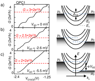
Figure 5a) shows the linear-response regime which is identical to the trace shown in Fig. 1a). A sketch of the energy landscape is shown at the right hand side. The parabolic electron dispersions are energetically separated by the subband spacing due to transversal confinement. In the depicted situation, three subband-bottoms reside below the chemical potentials of source and drain, giving rise to a conductance of . Figure 5b) shows the pinch-off trace for , where plateaus appear at half-integer values of the conductance. The sketch corresponding to a conductance of is shown on the right hand side: two subbands contribute fully and one subband contributes half to the overall conductance.
So-called half-plateaus can only be observed in clean samples, presumably because scattering events inside the QPC become more likely when more unoccupied subband states are energetically available at larger source-drain bias. At even higher bias, the conductance is usually obscured by noise [22] or it increases/decreases due to various self-gating effects [13, 20]. In QPC1 however, the return of integer conductance quantization for two subband bottoms residing in-between and is observable in Fig. 5c) at . We interpret this observation as another result of the cleanliness of the QPC which reduces the probability for backscattering.
In order to retrieve the full information about the confinement potential, the transconductance of QPC1 is plotted in Fig. 6a) as a function of and .
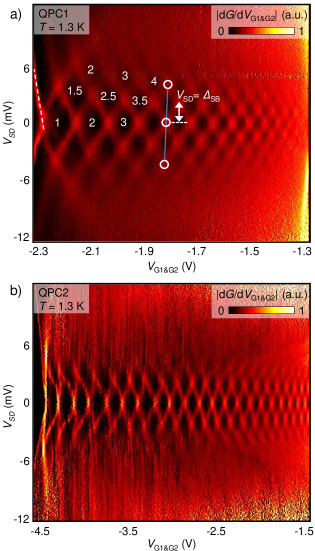
Integer conductance plateaus without subband minima between and (labeled ), appear as black diamonds around . Half plateaus () and second order integer plateaus () appear in a regular pattern at finite source-drain bias.
In our experience, the higher order plateaus can not be observed in samples with mobility (cf. [22]). Comparing our data to data of a defect-free QPC [21] defined in a 2DEG with mobility , we find subtle differences in the transconductance pattern. Although the QPC in reference [21] is measured at a lower temperature () than our device (), second order integer plateaus seem to be suppressed as long as no magnetic field is applied perpendicular to the 2DEG. The authors state that “Due to the suppression of backscattering in the presence of a small magnetic field the reappearance of the integer plateaus at high can be clearly observed”. Our QPC is defined in a 2DEG with mobility and second order integer plateaus are clearly resolved at . These observations indicate that even though the mean free path of the electrons is much larger than the length of the QPC in both cases, a higher electron mobility still manifests itself as reduced backscattering in the regime of nonlinear conductance.
As seen from the sketches in Fig. 5, the maximum extent of the diamonds in corresponds to the energy spacing of the involved QPC subbands. The whole pattern of transconductance diamonds is sheared with features at positive shifted by about to more positive gate voltage than in a perfectly symmetric configuration. This asymmetry could hint at a slight asymmetry of the QPC’s coupling to source and drain but might also be explained by a gradual drift of the local potential over the measurement time of .
The effect of onto the confinement potential, the so-called self-gating, manifests itself as a deviation from a pattern of straight lines [13]. From Fig. 6a) it appears that self-gating plays an important role mainly close to pinch-off (white dashed line) and perhaps at very large , where no clear quantization is observed any more. Since self-gating appears not to dominate the shape of the transconductance pattern it is possible to learn more about the confinement potential by comparing the position of transconductance nodes in Fig. 6a). Three exemplary nodes are highlighted by white circles. They correspond to the resonance conditions (from top to bottom) (), () and (), respectively. The fact that these resonance conditions occur at almost the same gate voltage (along a straight line) means that the subband-spacings and are very similar at this gate voltage (compare sketches in Fig. 5). Therefore the transversal confinement can be well described by a harmonic potential. If the confinement potential were for example a square well, the subband spacings would increase with higher mode number and hence the higher order modes would occur at more positive gate voltage than the linear response node.
As a comparison to the clean and regular pattern of QPC1, Figure 6b) shows the transconductance of QPC2. Higher order plateaus are visible for but are obscured by noise at more negative bias which is usually related to tunneling events from the gates into the doping layer [23]. Furthermore, the shape of the five leftmost diamonds is distorted with the upper and lower tip being shifted to more negative gate bias. This shift as well as the curvature of the plateau borders follows the dependence observed in quantum wires and arises from the requirement of satisfying charge neutrality with a 1-dimensional density of states while applying a finite source-drain voltage [24]. The quantum wire-like characteristic is consistent with the geometry of the gates which should create a channel that is longer than the screening length of the 2DEG (compare inset of Fig. 1b)). It is noteworthy that also in the quantum wire-like QPC2, we observe a well pronounced half-plateau related to the 0.7-anomaly which resembles the features observed in [24]. Since we do not observe defect-related resonances in QPC2, the design might be extended to even longer gate-defined quantum wires [25, 26, 27] in order to study the length-dependence of the 0.7-anomaly. However, the observation of diffusive transport [26] in long quantum wires (with the mean free path in the 2DEG being ) suggests that gate-defined quantum wires might not profit from an increased free electron mobility at least if split-gate technology is used for confinement.
2.4 Extracting the QPCs’ Shape Parameters
As discussed earlier, the transconductance plot can now be used to reconstruct the confinement potential. The subband spacing can be determined from the position of the borders of the transconductance diamonds [20]. Due to the finite resistance of the leads , a fraction of the applied DC-bias does not drop at the QPC. Using and the measured four-terminal conductance , this is taken into account via . The thereby determined subband spacings are plotted as a function of in Fig. 7a) for QPC1 (left) and QPC2 (right).
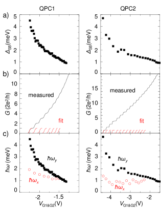
The subband spacings increase monotonically with more negative gate bias, indicating that the confinement potential becomes narrower and steeper while approaching pinch-off. This trend has been observed before [20] and can be explained by the reduced influence of screening on the confinement potential when the local electron density is reduced [28]. Since the higher order plateaus indicate that the confinement potential of QPC1 has a close-to harmonic shape, we can now use the measured subband spacings to apply Büttiker’s saddle-point model [29] to our linear response data and extract all parameters of the potential profile at the constriction. Since QPC2 shows quantum wire-like transport characteristics, the model is not expected to reflect the exact potential shape of QPC2, but should still give qualitatively meaningful results. Temperature broadening is not accounted for in this model since the subband-spacings are much larger than the thermal broadening .
Neglecting inter-mode scattering and including spin degeneracy, the transmission of the -th subband is given by
| (1) |
with the energy of the -th subband
| (2) |
The gate dependence is known from Fig.7a), the gate dependence of the conduction band bottom is approximated by for each conductance step with the lever arm converting gate voltage to energy. Usually, the lever arm can be determined by taking the source-drain bias as an energy reference and comparing it to the gate dependence of a given transport resonance [30]. But as shown in Fig.7a), the gate voltage not only lifts but also increases the subband spacing, giving rise to a seemingly increased lever arm. Knowing that the confinement potential is harmonic enables an alternative way to determine . At the position of the conductance steps in Fig.7a) (at ), the conduction band bottom is below the Fermi energy. Hence, the lever arm in-between two successive steps is given by
| (3) |
with being the confinement at the -th step as extracted from Fig.7a). Now the only fitting parameters are the longitudinal curvature and the energy offset .
Figure 7b) shows the pinch off curve of QPC1 (left) and the fits resulting from the described procedure. All fits are plotted below for clarity. The same procedure applied to QPC2 is shown on the right hand side. Figure 7c) shows the extracted values for the longitudinal curvature (circles) of QPC1 (left) and QPC2 (right). The transversal curvature is plotted as squares for comparison. In both QPCs, is smaller than , as required for the observation of conductance quantization [29]. Approaching pinch-off, QPC1 becomes much narrower (strong increase of ) and slightly shorter (increase of ). QPC2 also becomes much narrower but there is no strong increase of . Although the saddle-point model might not be the ideal model for a quantum wire, this fits the intuitive picture of a 1-dimensional channel with a lithography-defined length and voltage-controlled width.
Comparing the parameters obtained from our analysis to those from earlier investigations, we find surprising discrepancies despite similar 2DEG density and gate-spacings. The data analyzed in [31] is well described by , with both values being independent of gate voltage. In our devices, the shape of the confinement potential changes dramatically as a function of gate voltage and reaches oscillator strengths of , close to pinch-off. We interpret this observation as the result of the screening properties of the screening layers that are grown into the heterostructure in order to achieve ultra-high electron mobilities [6, 7, 8]. Screening should reduce the range of the gate-induced potential and thereby increase the slope of the confinement potential.
2.5 Spin-Resolved Transport at Low Temperatures
Additional changes in the confinement can be created by applying a magnetic field perpendicular to the plane of the 2DEG which lifts the spin degeneracy and increases the subband spacing [1, 32, 21, 12, 9]. QPC3 was not equipped with a 2DEG terminal that could be used to measure the diagonal voltage, so the filling factor of the QPC is calculated from the longitudinal four-terminal resistance: In analogy to magnetotransport through a barrier [33], relates via to the number of occupied Landau levels in the bulk . Knowing the electron density and Planck’s constant , the measured four-terminal resistance can be directly converted to . Figure 8a) shows data of QPC3 (split-gate gap ), measured at a temperature of with .
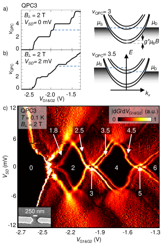
Plotting as a function of reveals integer filling factors related to the magneto-electric subband spacing (, ) but also smaller plateaus due to the lifted spin degeneracy (, ). The energy diagram corresponding to is shown on the right hand side. The lowest spin-split plateau is obscured by the 0.7 anomaly [12]. The same trace repeated at finite source-drain bias is shown in Fig. 8b). Additional half-plateaus with and appear which correspond to a situation as depicted to the right: one spin-split mode is situated in-between and . The 0.7 anomaly has evolved into a plateau with . Figure 8c) shows a false color plot of the transconductance , plotted as a function of and . Similar to the transconductance plots in Figs. 6, regions of integer filling factor appear as black diamonds. Due to the different sizes of the subband-split levels (labeled 2, 4 and 6) and the spin-split levels (3 and 5), the half-plateaus at finite appear as black stripes. A clear deviation from the regular even-odd pattern is observed at low filling factors, where are replaced by a plateau related to the 0.7 anomaly.
From the extent of the spin-split plateaus the exchange-enhanced -factor can be extracted via , where is the effective -factor and denotes the Bohr magneton. Compared to the bare -factor of GaAs (), we find a strongly enhanced at and at . Similar to findings of Thomas at al. [12], increases with lower mode number. However, the magnitude of the exchange enhancement is different: was reported by Thomas at al., while our results indicate a much stronger enhancement. Assuming that disorder reduces the effectiveness of the exchange enhancement, the observation of strongly enhanced -factors can be interpreted as another manifestation of the good sample quality.
3 Conclusion
In conclusion, we investigated the transport properties of two differently shaped constrictions that were defined within a high-mobility 2DEG. Transport spectroscopy in the linear response regime demonstrates that conductance quantization is observed and that no scattering centers are found when shifting QPC1 between the gates. The 0.7-anomaly is investigated by varying the temperature and by applying a magnetic field perpendicular to the 2DEG. Depending on the ratio of these two parameters we observe either a weakening or an enhancement of the 0.7-anomaly which is discussed in view of spin-polarized edge channels mimicking the 0.7 scenario. Measurements at finite source-drain bias give access to the subband spacings of the QPC and reveal that QPC1 is described best by a short constriction whereas QPC2 shows quantum wire-like characteristics. In addition to QPCs defined in standard 2DEGs, resonances at large bias are observed in QPC1 that correspond to higher order transport conditions. These higher order resonance conditions give valuable information about the shape of the confinement potential and enable the reconstruction of the full saddle point potential in the constriction. Knowing the shape (and hence the slope) might prove important for the investigation of many body states like the 0.7 anomaly or the transmission of fractional quantum Hall states. At finite magnetic field and lower temperature, a strongly exchange-enhanced -factor is observed which we interpret as the result of a very smooth confinement potential. While the measurements on QPCs are possible with high signal to noise ratio if the gate voltages are always swept in the same regime and direction, it was not possible to form a stable quantum dot with the same technique on the same wafer. For future interferometer experiments on high-mobility samples in the fractional quantum Hall regime it is desirable to prepare split-gate electrodes on high-mobility wafers that do not rely on screening electrons at the X-valley and thereby allow stable gate operation.
4 Acknowledgments
We acknowledge the support of the ETH FIRST laboratory and financial support of the Swiss Science Foundation (Schweizerischer Nationalfonds, NCCR Nanoscience).
References
References
- [1] Wharam D A, Thornton T J, Newbury R, Pepper M, Ahmed H, Frost J E F, Hasko D G, Peacock D C, Ritchie D A and Jones G A C 1988 J. Phys. C.: Solid State Phys. 21 L209
- [2] van Wees B J, van Houten H, Beenakker C W J, Williamson J G, Kouwenhoven L P, van der Marel D and Foxon C T 1988 Phys. Rev. Lett. 60 848
- [3] Willett R, Eisenstein J P, Störmer H L, Tsui D C, Gossard A C and English J H 1987 Phys. Rev. Lett. 59 1776
- [4] Miller J B, Radu I P, Zumbühl D M, Levenson-Falk E M, Kastner M A, Marcus C M, Pfeiffer L N and West K W 2007 Nature Physics 3 561
- [5] Dolev M, Heiblum M, Umansky V, Stern A and Mahalu D 2008 Nature 452 829
- [6] Friedland K-J, Hey R, Kostial H, Klann R and Ploog K 1996 Phys. Rev. Lett. 77 4616
- [7] Umansky V, de Picciotto R and Heiblum M 1997 Appl. Phys. Lett. 71 683
- [8] Hwang E H and Sarma S D 2008 Phys. Rev. B. 77, 235437
- [9] Rössler C, Feil T, Mensch P, Ihn T, Ensslin K, Schuh D and Wegscheider W 2010 N. J. Phys. 12 043007
- [10] Williamson J G, Timmering C E, Harmans C J P M, Harris J J and Foxon C T 1990 Phys. Rev. B. 42 7675 (R)
- [11] The magnitude of the QPC-shift has been independently verified via low-temperature scanning gate microscopy; Schnez S et al., arXiv:1109.1544v1
- [12] Thomas K J, Nicholls J T, Simmons M Y, Pepper M, Mace D R and Ritchie D A 1996 Phys. Rev. Lett. 77 135
- [13] Kristensen A, Bruus H, Hansen A E, Jensen J B, Lindelof P E, Marckmann J C, Nygard J, Sorensen C B, Beuscher F, Forchel A and Michel M 2000 Phys. Rev. B. 62 10950
- [14] Cronenwett S M, Lynch H J, Goldhaber-Gordon D, Kouwenhoven L P, Marcus C M, Hirose K, Wingreen N S and Umansky V 2002 Phys. Rev. Lett. 88, 226805
- [15] Hatke A T, Zudov M A, Pfeiffer L N and West K W 2011 Phys. Rev. B 83, 081301(R)
- [16] Shailos A, Bird J P, Lilly M P, Reno J L and Simmons J A 2006 J. Phys. Cond. Mat. 18, 3277
- [17] Komijani Y, Csontos M, Shorubalko I, Ihn T, Ensslin K, Meir Y, Reuter D and Wieck A. D. 2010 EPL 91, 67010
- [18] Glazman L I and Khaetskii A V 1989 Europhys. Lett. 9 263
- [19] Patel N K, Martin-Moreno L, Pepper M, Newbury R, Frost J E F, Ritchie D A, Jones G A C, Janssen J T M B, Singleton J and Perenboom J A A J 1990 J. Phys. C 2, 7247
- [20] Patel N K, Nicholls J T, Martin-Moreno L, Pepper M, Frost J E F, Ritchie D A and Jones G A C 1991 Phys. Rev. B 44 13549
- [21] Thomas K J, Simmons M Y, Nicholls J T, Mace D R, Pepper M and Ritchie D A 1995 Appl. Phys. Lett. 67, 109
- [22] Rössler C, Herz M, Bichler M and Ludwig S 2010 Solid State Comm. 150 861
- [23] Pioro-Ladriere M, Davies J H, Long A R, Sachrajda A R, Gaudreau L, Zawadzki P, Lapointe J, Gupta J, Wasilewski Z and Studenikin S 2005 Phys. Rev. B 72 115331
- [24] de Picciotto R, Pfeiffer L N, Baldwin K W and West K W 2004 Phys. Rev. Lett. 93 36805
- [25] Tarucha S, Honda T and Saku T 1995 Solid State Comm. 94 413
- [26] Liang C-T, Simmons M Y, Smith C G, Ritchie D A and Pepper M 1999 Appl. Phys. Lett. 75 2975
- [27] Morimoto T, Henmi M, Naito R, Tsubaki K, Aoki N, Bird J P and Ochiai Y 2006 Phys. Rev. Lett. 97 096801
- [28] Laux S E, Frank D J and Stern F 1988 Surf. Sci. 196 101
- [29] Büttiker M 1990 Phys. Rev. B 41 7906
- [30] Kouwenhoven L P, Austing D G and Tarucha S 2001 Rep. Prog. Phys. 64 701
- [31] Taboryski R, Kristensen A, Sorensen C B and Lindelof P E 1995 Phys. Rev. B 51 2282
- [32] van Wees B J, Kouwenhoven L P, van Houten H, Beenakker C W J, Mooij J E, Foxon C T and Harris J J 1988 Phys. Rev. B 38 3625 (R)
- [33] Haug R J, MacDonald A H, Streda P and von Klitzing K 1988 Phys. Rev. Lett. 61 2797