A Design Methodology for Folded, Pipelined Architectures in VLSI Applications using Projective Space Lattices
Abstract
Semi-parallel, or folded, VLSI architectures are used whenever hardware resources need to be saved at design time. Most recent applications that are based on Projective Geometry (PG) based balanced bipartite graph also fall in this category. In this paper, we provide a high-level, top-down design methodology to design optimal semi-parallel architectures for applications, whose Data Flow Graph (DFG) is based on PG bipartite graph. Such applications have been found e.g. in error-control coding and matrix computations. Unlike many other folding schemes, the topology of connections between physical elements does not change in this methodology. Another advantage is the ease of implementation. To lessen the throughput loss due to folding, we also incorporate a multi-tier pipelining strategy in the design methodology. The design methodology has been verified by implementing a synthesis tool in C++, which has been verified as well. The tool is publicly available. Further, a complete decoder was manually protototyped before the synthesis tool design, to verify all the algorithms evolved in this paper, towards various steps of refinement. Another specific high-performance design of an LDPC decoder based on this methodology was worked out in past, and has been patented as well.
Keywords: Design Methodology, Parallel Scheduling and Semi-parallel Architecture
1 Introduction
A number of naturally parallel computations make use of balanced bipartite graphs arising from finite projective geometry [13], [1], [22], [16], and related structures [17], [18], [15] to represent their data flows. Many of them are in fact, recent research directions, e.g. [13], [17], [16]. As the dimension of the finite projective space is increased, the corresponding graphs grow both in size and order. Each vertex of the graph represents a LPU, and all the vertices on one side of the graph compute in parallel, since there are no data dependencies/edges between vertices that belong to one side of a bipartite graph. The number of such parallel LPUs is generally of the order of tens of thousands in practice for various reasons as noted below.
It is well-known in the area of error-control coding that higher the length of error correction code, the closer it operates to Shannon limit of capacity of a transmission channel [16]. The length of a code corresponds to size of a particular bipartite graph, Tanner graph, which is also the data flow graph for the decoding system [16]. Similarly, in matrix computations, especially LU/Cholesky decomposition for solving system of linear equations, and iterative PDE solving (and the sparse matrix vector multiplication sub-problem within) using conjugate gradient algorithm, the matrix sizes involved can be of similar high order. A PG-based parallel data distribution can be imposed using suitable interconnection of processors to provide optimal computation time [22], which can result in quite big setup (as big as a petaflop supercomputer). This setup is being targeted in Computational Research Labs, India, who are our collaboration partners. Further, at times, increasing the dimension of finite projective geometry used in a computation has been found to improve application performance [1]. In such a case, the number of LPUs grows exponentially with the dimension again. For practical system implementations with good application performance, it is generally not possible to have a large number of LPUs running in parallel, since that incurs high manufacturing costs. In VLSI terms, such implementations may suffer from relatively large area, and are also not scalable. Here, scalability captures the ease of using the same architecture for extensions of the application that may require different throughputs, input block sizes etc. A folded architecture can generally provide area reduction and scalability as advantages instead, while trading off with system throughput. We have therefore focused on designing semi-parallel, or folded architectures, for such PG-based applications.
The applicability of such schemes may not be that widespread, given the current ULSI levels of integration. Still, there are application areas in ASIC design, where direct interconnect is still more pertinent (e.g., [1] and [26]). This is because the required interconnect is a sparse interconnect. In fact, most practical designs reported here are of semi-parallel nature. With such applications in mind, we a folding scheme over next few sections.
As such, folding of VLSI architectures especially for communications and signal processing systems is has been well-known [19]. However, the algorithms involved, such as register minimization algorithms, are generic in nature, and at times, iterative. We present much simpler set of algorithms for folding for the target class of applications.
In this paper, we first present a scheme for folding PG-based computations efficiently, which allows a practical implementation with the following advantages.
-
1.
The number of on-chip logical processing units required, is reduced.
-
2.
No processing unit is ever idle in a machine cycle.
-
3.
A schedule can be generated which ensures that there are no memory access conflicts between logical processing units, for each (logical) memory unit.
-
4.
The same set of wires can be used to schedule communication of data between memory units and processing units that are physically used across multiple folds, without changing their interconnection.
-
5.
Data distribution among the memories is such that the address generation circuits are simplified to counters/look-up tables.
As an additional advantage of using this folding scheme, the communication architecture can be chosen to be point-to-point. This is because same set of wires can be reused across multiple folds, due to overlay (i.e., without reconfiguring their end points at run time). This significantly reduces the amount of wiring resources that are needed physically. Hence, a point-to-point interconnection becomes generally feasible after such folding. Such overlay-based custom communication architecture leads to optimal performance, as will be brought out in the paper. Generally, folding leads to overlay of computation, while here, it simultaneously leads to overlay of communication. Hence this scheme can also be alternatively viewed as one of evolving custom communication architecture.
In general, custom communication architectures attempt to address the shortcomings of standard on-chip communication architectures by utilizing new topologies and protocols to obtain improvements for design goals, such as performance and power. These novel topologies and protocols are often customized to suit a particular application, and typically include optimizations to meet application-specific design goals. In our case, the foldable point-to-point communication is optimized towards PG-based applications pointed out earlier.
This scheme forms the core of the design methodology that is our main contribution. The scheme is based on simple concepts of modulo arithmetic, and circulance of PG-based balanced bipartite graphs. It is an engineering-oriented, practical alternative to another scheme based on vector space partitioning [9]. The core of that scheme is based on adapting the method of vector space partitioning [5] to projective spaces, and hence involves fair amount of mathematical rigor. A restricted version of that scheme, which partitions the vector space in a novel way, was worked out earlier using different methods [8]. All this work was done as part of a research theme of evolving optimal folding architecture design methods, and also applying such methods in real system design. As part of second goal, such folding schemes have been used for design of specific decoder systems having applications in secondary storage [23], [1].
The target of this design methodology is to design specialized IP cores, rather than a complete SoC. The methodology uses four levels of model refinements. The level of details at these refinement levels turn out to be very similar to the four levels in SpecC system-level design methodology by Gajski et al [10]. Details of this similarity are provided in section 8. The latter methodology was targeted for bus-based system designs. Still, the similarity points to the fact that implementing a practical, custom synthesis-based design flow for this methodology can indeed be worked out. We have chosen to use the synthesizable subset of any popular HDL, to model various sub-computations of various overall PG-based computations, for whom we intend to automatically design (various) folded architectures. Practically, the custom design flow for this design methodology must hand over at some point, RTL models to e.g. some standard ASIC/FPGA design flow. A case study of successfully using this design flow for prototyping a VLSI system is described in section 11. The section also presents some details about the C++ tool that has been implemented, to realize this methodology.
In this paper, we begin by giving a brief introduction to Projective Spaces in section 2, which is easy to grasp. It is followed by a model of the nature of computations covered, and how they can be mapped to PG based graphs, in section 3. Section 5 introduces the concept of folding for this model of computation. The basic constructs for optimal scheduling, perfect access patterns and sequences are introduced in section 4. Section 5.1 sketches out what kind of folding is desired from regular bipartite graphs, while section 6 brings out how PG-based balanced regular bipartite graphs can be folded so, optimally. The details of various aspects of the design methodology are brought out in section 7 next. Especially, section 7.4 covers the detailed design problems that are enlisted in section 7.3. A scheme for pipelining the folded designs to recover back some throughput, that is lost due to trade-off, is covered in sections 7.5.1. In section 8, we bring out the practical way of using this methodology. A note on addressing scalability concern in our design is provided in section 9. We provide specifications of some real applications that were built using this methodology, in the experiments section (section 11), before concluding the paper.
2 Projective Spaces
Projective spaces and their lattices are built using vector subspaces of the bijectively corresponding vector space, one dimension high, and their subsumption relations. Vector spaces being extension fields, Galois fields are used to practically construct projective spaces [1]. However, throughout this work, we are mainly concerned with subgraphs arising out lattice representation of Projective spaces, which we discuss now. An overview of generating projective spaces from finite fields can be found in A.
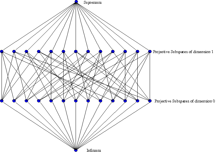
It is a well-known fact that the lattice of subspaces in any projective space is a modular, geometric lattice [9]. A projective space of dimension 2 is shown in figure 1. In such figure, the top-most node represents the supremum, which is a projective space of dimension m over Galois Field of size q, in a lattice for . The bottom-most node represents the infimum, which is a projective space of (notational) dimension -1. Each node in the lattice as such is a projective subspace, called a flat. Each horizontal level of flats represents a collection of all projective subspaces of of a particular dimension. For example, the first level of flats above infimum are flats of dimension 0, the next level are flats of dimension 1, and so on. Some levels have special names. The flats of dimension 0 are called points, flats of dimension 1 are called lines, flats of dimension 2 are called planes, and flats of dimension (m-1) in an overall projective space are called hyperplanes. Many PG-based applications have models that are based on two levels in this diagram, and connections based on their inter-reachability in the lattice. Out of these, the balanced regular bipartite graphs made out of levels of points and hyperplanes have been used more often, because usually the applications require the graph to have a high node degree, which this graph provides.
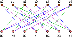
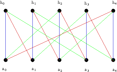
2.1 Circulant Balanced Bipartite Graph
A circulant balanced bipartite graph is a graph of n graph vertices on each side, in which the graph vertex of each side is adjacent to the graph vertices of other side, for each j in a list L of vertex indices from other side. A point-hyperplane incidence bipartite graph made from PG lattice is a circulant graph; see Fig. 2. We will be exploiting the circulance property of PG bipartite graphs in our folding scheme.
As will become clear from the constructive proof of main theorem 1, this scheme can be extended to cover design of any system, whose DFG exhibits a bipartite circulant nature, of any order. However, a practical design methodology must target design of real systems. Hence we stick to PG-based applications as our target real application area of this design methodology.
3 A Model for Computations Involved
As mentioned earlier, we will be using a PG bipartite graph made from points and hyperplanes in a PG lattice. In such graph, each point, as well as hyperplane, is mapped to a unique vertex in the graph. Further, a point and a hyperplane are incident on one-another in this bipartite graph, if they are reachable via some path in the corresponding lattice diagram. We state without proof, that such bipartite graph is both balanced (both sides have same number of nodes) and regular (each node on one side of graph has same degree). For the proof, see [25].
The computations that can be covered using this design scheme are mostly applicable to the popular class of iterative decoding algorithms for error correcting codes, like Low-density Parity-check (LDPC) [3], polar [2] or expander codes [27]. A representation of such computation is generally available as a bipartite graph, though it may go by some other domain-specific name such as Tanner Graph. The nodes on each side of the bipartite graph represent sub-computations (sequential circuits), which do not have any precedence orders. Hence they can all be made to execute computations parallely. The edges represent the data that is exchanged between nodes performing sub-computations. Also, the nature of computation algorithm being considered is such that nodes on one side of the graph compute first, then nodes on the other side of the graph. If the computation is iterative, then the computation schedule so far is just repeated again and again. Such a schedule is popularly known as flooding schedule, since all nodes of one side simultaneously send out data to nodes on other side. A bipartite graph is undirected, and hence for visualization as a Data Flow Graph (DFG), each of its edge can be replaced with two opposite-directed edges. Such an expansion is depicted in figure 3. Such a refinement of problem model is only for conceptual clarity, and not implemented in the corresponding design flow. Such a DFG may model both SIMD as well as MIMD systems. Since we target design of PG-based applications using this methodology, we assume throughout the remaining text that
-
1.
The nature of parallel computation is SIMD.
-
2.
The computation function realized by any node, is any computation that can be realized using the a particular synthesis subset of various HDLs, described in section 4.2.
Relaxing these assumptions leads to a tradeoff between optimality of system performance, and ease of system implementation. Details of this tradeoff can be found in section 4.2.
After finishing the computations, nodes on any one side of the bipartite graph transfer the resultant data for consumption of nodes on other side of the graph, via distributed storage in memory units. Usage of distributed memory is common and fundamental requirement to folding the graph using this method. Thus, one LMU per node, just before its input along the data flow direction, is the minimum requirement for storing data which is transferred within a bipartite graph111At times, to implement interconnect pipelining to reduce signal delays in practical physical design of such systems, memory elements may also be present at the output.. An easy way of implementing distributed memory on both sides is to collocate local/on-chip memory of each physical node with each required PMU.
4 Conflict-free Communications Primitives for PG Graphs
The scheduling model used in the folding scheme is based on Karmarkar’s template[14]. PG lattices possess structural regularity in form of circulance, and this property has been exploited in scheduling of general parallel systems. Karmarkar was able to come up with a parallel communication method to realize various “nice properties” in scheduling, which are enlisted later in the section. He discovered two memory-conflict free communication primitives using bipartite graphs derived from 2-dimensional Projective Space Lattices [14].
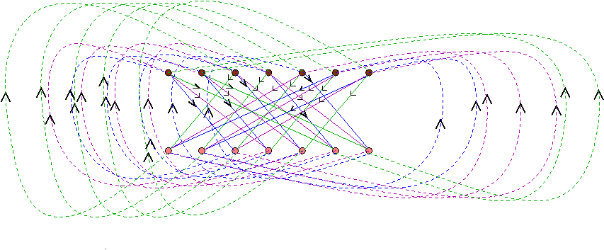
Let n processing units be placed in place denoted by the lines, and n memory units placed in place denoted by the points, in a PG bipartite graph. Consider a binary operation that is to be scheduled on these processing units in SIMD fashion. Let it take two operands as inputs (reads from two memory locations) per cycle, and modify one of them (writes back in one memory location) as output. The binary operation is preferred since the required memory unit is then a dual-port memory, something that is easily commercially-off-the-shelf (COTS) available. The schedule of memory accesses for a collection of such operations, that corresponds to a particular complete set of line-point index-pairs, for simultaneous parallel execution over one cycle on all processing units is known as a Perfect Access Pattern. A set of such patterns, with some application-defined order imposed on them, is known as a Perfect Access Sequence. Such particular complete set of line-point index pairs is generated by exploiting circulant nature of PG bipartite graph. On each node on one side of the graph, two edges are chosen such that they are shift-replicas of the two edges chosen for its neighboring node. For example, in figure 4, the set of 13 red and 13 green edges forms one Perfect Access Pattern, and 13 yellow and 13 blue edges another Perfect Pattern. These two perfect patterns (like these two), when sequenced in arbitrary order, form a Perfect Access Sequence. The properties of such an execution of processing unit-memory unit communication are as follows [14].
-
1.
There are no read or write conflicts in memory accesses.
-
2.
There is no conflict or wait in processor usage.
-
3.
All processors are fully utilized.
-
4.
Memory bandwidth is fully utilized.
4.1 Generalization
The cost of a perfect access sequence is cycles, where is the degree of each node in bipartite graph. There can be possibly alternative communication primitives, which can have different communication costs over the same projective plane. Generalizing beyond binary operation scheduling to n-ary operation scheduling on computing nodes reduces the communication cost, but leads to complexity of the memory unit controller’s design/area/power.
Practically, there are many parallel computational problems, implementable in hardware, whose communication graph has been derived out of higher-dimensional projective spaces. Two such problems, that were worked out by us, are LU decomposition (exploiting a 4-dimensional underlying projective space) [22], and the DVD-R decoder (exploiting a 5-dimensional underlying projective space) [1]. In [24], it is proven in detail that Karmarkar’s scheme of decomposing a projective plane into perfect access patterns can indeed be extended to point-hyperplane graphs of arbitrary dimensional Projective Space. For sake of brevity, the proof is not repeated here.
4.2 Suitability of Perfect Access Patterns for Other Computations
We explain now that any synthesizable sequential logic can represent the computation meant by the ‘single instruction’ in SIMD model, as long as in its multi-input Mealy machine representation, each transition is governed by arrival of a particular input signal, and not on the value of the signal. Thus, in a given state, we assume that such FSM, in a given state, accepts a compatible signal arrival event, transitions into a unique state, and optionally outputs a unique set of signals, irrespective of the value of the input signal. In our computation model, each input edge incident on a vertex is treated as a signal. Multiple inputs can arrive simultaneously in sequential logic, in which case the event is a compound signal event. Since we use SIMD model, the labeling of edges of all vertices on one side of bipartite graph, to represent signals, can be made isomorphic easily. Such labeling allows FSMs of all the node computations to move in synchronized fashion, requiring inputs in same sequence on all nodes on one side of bipartite graph. This is because FSM model of any sequential logic computation imposes a legal order requirement on its inputs , in order to reach its end state. Further, the legally ordered set of such inputs required by the ‘single instruction’ may not cover the complete set of possible inputs (edges) on each node. As long as same subset of inputs, in same sequence, is needed by each node to reach their end states, the collection of such subsequences can be used as a perfect access sequence required by the computation of ‘single instruction’. These subsequences must be synchronized at each clock cycle, for load balancing; there cannot be gaps in their scheduling. We can then break such common sequence into perfect access patterns, and use the basic result of folding a perfect access pattern (see theorem 1) to optimally schedule each such computations. Because we have the choice of picking up order while forming a perfect access sequence from the set of perfect access patterns (see section 4), we also have a choice in scheduling and ordering the input arrivals. Thus, we can always force the same order, as required by the sequential logic, on the perfect access ‘sequence’. A combinational logic computation is treated as a special case of sequential logic computation.
The application classes that we realistically target (described in section 1) have computations (e.g. accumulation operator), that naturally obey the restriction described above. Their multi-input Mealy machine model is a set of disjoint equal-length paths, between unique start and end states. The length of each path is , i.e. each legal input sequence to the state machine requires signals on all edges to arrive, in some permutation order, before completion of computation. The number of such paths in these models is equal to , though in our generalized model, it can be .
Going further, suppose we relax the SIMD assumption, and assume MIMD model of computation for the system under design. In such a case, there will be no restriction whatsoever on the sub-computation that is happening on each node in a particular cycle, and their computation times. The computations may be different, e.g. addition and subtraction. As long as all nodes on one side of the graph operate on the same number of operands at a time, and take same number of cycles to complete, the foldability of graph derived in this report will remain applicable. One may further relax the same computation time constraint on these sub-computations, by implementing a barrier synchronization on either side of the data flow graph. All such relaxations need to be annotated/added to the system model (Tanner Graph), and hence form the first level of refinement (specification refinement) of the DFG, which is an optional level. It is straightforward to notice that while applying this design methodology to MIMD systems retains the ease of engineering the system, as in SIMD case, there are chances that the system may lose some amount of performance optimality (e.g. due to mandatory barrier synchronization).
5 The Concept of Bipartite Graph Folding
Semi-parallel, or folded architectures are hardware-sharing architectures, in which hardware components are shared/overlaid for performing different parts of computation within a (single) computation. As such, folded architectures are a result of fundamental space-time complexity trade-off in (parallel) computation. This in turn manifests in form of area-throughput trade-off during its (parallel) implementation.
In its basic form, folding is a technique in which more than one algorithmic operations of the same type are mapped to the same hardware operator. This is achieved by time-multiplexing these multiple algorithm operations of the same type, onto single computational unit at system run-time. Hereafter, we define logical processing unit(LPU) as the logical computational unit associated with each node of the graph, while physical processing unit(PPU) as the physical computational unit associated with each node of the graph. Multiple LPUs get overlaid on single PPU, after folding. We also define the equivalent term for overlaid memory unit as physical memory unit(PMU), which is an overlay of multiple logical memory units(LMUs).
The balanced bipartite PG graphs of various target applications perform parallel computation, as described in section 3. In its classical sense, a folded architecture represents a partition, or a collection of folds, of such a (balanced) bipartite graph (see figure 5). The blocks of the partition, or folds can themselves be balanced or unbalanced; partitioning with unbalanced block sizes entails no obvious advantage. The computational folding can be implemented after (balanced) graph partitioning in two dual ways. In the first way, that is used in [8], [9], the within-fold computation is done sequentially, and across-fold computation is done parallely. Such a scheme is generally called a supernode-based folded design, since a logical supernode is held responsible for operating over a fold. Dually, the across-fold computation can be made sequential by scheduling first node of first fold, first node of second fold, sequentially on a single module. The within-fold computations, held by various nodes in the fold, can hence be made parallel by scheduling them over different hardware modules. This scheme is what we cover in this paper. Either way, such a folding is represented by a time-schedule, called the folding schedule. The schedule tells that in each machine cycle, which all computations are parallely scheduled on various PPUs, and also the sequence of clusters of such parallel computations across machine cycles.
5.1 Folding PG-based Bipartite Graphs
We first sketch out, how a PG bipartite graph can be folded. Generally folding is performed by partitioning the vertex sets of the bipartite graph, and overlaying them on various available PPUs. As such, general folding schemes are not able to overlay the edge sets onto each other. It potentially results in reconfiguring the interconnection between physical units at run-time, whenever a new fold has to be scheduled. What stands out in case of using our folding scheme is that edges also get overlaid. Hence the entire run-time overhead of reconfiguring the interconnect via various mux selections is saved.
In a PG balanced bipartite graph made from points and hyperplanes of -dimensional projective space over , , the number of nodes on either side is = , while the degree of each node is = . Here, p is any prime number, while s is any natural number. For vertex partitioning, as discussed earlier, we choose to have e.g. PPU performing left node computation in a cycle, then left node computation in next cycle, and so on. By doing so, it so happens, as we prove later, that the destination vertex of each edge incident on various nodes across various partitions of one side of the graph, that are mapped to same PPU post folding, remains identical. Due to dual-port memory unit restriction, the computation by each PPU can only be performed across multiple cycles (2 inputs possible per cycle). Hence we also need to partition the edge set of each node, generally into subsets of 2 edges, as depicted in figure 4.
By applying perfect access patterns and sequences [14] for inter-unit communication, that are applicable for all possible point-hyperplane bipartite graphs, the overlaid edge partitioning mentioned above can be readily achieved. Recall that a perfect access pattern stimulates only a fraction of edges per node in a cycle. Hence we focus our efforts on evolving the vertex partitioning only. For practical designs, to avoid 2 concurrent accesses to a memory unit in a machine cycle, we assume that edge-partitioning has already been done (forming perfect access sequence), and that we are trying to do a vertex partitioning over each Perfect Access Pattern within the sequence. Further, in vertex partitioning, as reasoned earlier, we focus on creating balanced, equal-factor partitions only; refer figure 5. However, the methodology can be extended easily to handle unequal-factor folding of both sides as well.
6 Core Folding Scheme
In the subsequent text, we assume that associated with each node or PPU, there is one (distributed) PMU, using which data can be transferred across the bipartite graph for computation. We have already mentioned this assumption before, in section 3. To recall from 1, logical processing unit (LPU) is defined as the logical computational unit associated with each node of the graph, while physical processing unit (PPU) as the physical computational unit associated with each node of the graph. The equivalent term for overlaid memory unit is physical memory unit (PMU), which is an overlay of multiple logical memory units (LMUs). Hence in the initial architecture, there are J LPUs and LMUs of one type, and another J LPUs and LMUs of another type. This architecture represents the second level of refinement222first mandatory, to-be-implemented level of refinement of the data flow graph, and is more detailed in section 7.1. As per the model of computations to be scheduled on this architecture (section 3), LPUs of one type need to read their input data from LMUs of the other type. The core problem that we tackle first is to prove that using an equal number of LPUs and LMUs, where the number is any factor of J, and interconnecting them in specific way, the necessary data flow between them in an unfolded PG bipartite graph based computation can still be achieved optimally. We build the design methodology around this main result.
6.1 Problem Formulation
Suppose we fold both sets of nodes by a factor of q in a PG balanced bipartite graph. Hence there are J/q PPUs and PMUs of either type. Since overall number of edges in the non-folded regular bipartite graph is ( defined in section 5.1), the required size of each PMU to store all data corresponding to these many edges is . Our unit of computation is a fold of one row of nodes, each of which has inputs/outputs. If this fold were to impose uniform load/storage requirements on each of the J/q memories, then the uniform (storage/communication) load imposed by outputs of J/q PPUs on J/q PMUs is trivially .
Given that we have J/q PPUs and PMUs physically available, one question is whether it is possible to generate perfect patterns using J/q elements of either type (PPUs or PMUs). If this were true, then it will lead to uniform load () on the J/q PMUs, since we know that perfect access patterns impose balanced loads [14]. Combining such patterns will give a perfect access sequence. We discuss some possible approaches to this question now.
To have a embedded perfect access pattern, one option is that J/q nodes of both types, and their interconnection becomes a embedded PG sub-geometry in itself. For that, J/q must take a value of form for some prime and non-negative integer . This is the cardinality of the set of hyperplanes in some . In such a case, we would need to study such structure-ability of J for various values of p (its base prime) and q (its desired factors).
If this were possible, node connectivity of such embedded geometry, from first principles, will be [14]. However, each node needs all of inputs, where is order of the base Galois field of n-dimensional projective space under consideration, for otherwise, their computation will be incomplete.
As an example, let = 3 and = 2. Then = 91 and = 10. Now = 7 is a factor of 91. If we fold each row of node 7 times, then J/q = 13. An order-13 regular bipartite graph is possible when = 3 and = 1. However, by definition, such a smaller graph has its regular node degree = 4, while we need it to be 10 itself.
The solution lies in simply increasing the LMU size and number of accesses per LMU. As one can see, in general for projective spaces over non-binary Galois Fields, is divisible by 2. When we take 2-access at a time, we can form a perfect access pattern in the J/q-sized fold of a regular bipartite graph as detailed in theorem 1, for ANY q. We later easily extend the same pattern generation for graphs derived from projective spaces based on binary Galois Fields.
6.2 Folding by ANY Factor
We now generalize our earlier analysis suitably and make the final statement.
Theorem 1.
It is possible to generate a (folded) perfect access pattern, from a non-folded perfect access pattern, using J/q LPUs and LMUs of a fold that belongs to the bipartite graph based on , for ANY q that divides J.
Proof.
The two important properties used in this proof are properties of modulo addition, and circulance of PG-based balanced bipartite graph. As mentioned earlier, PG-based bipartite graph is a circulant graph.
For all notations as well as all representative indices that we use hereafter in the paper, we follow figure 6. Let the unfolded set of computations (hyperplanes) be represented as . After folding, let the new set of LPUs be represented as . Similarly, let the unfolded set of storages (points) be represented as . After folding, let the new set of dual-port LMUs be represented as . Given a subgraph which corresponds to any one full (non-folded) perfect pattern which has to be vertex-folded, let some two edges of some node marked by be and .
Overall, being the first node in the fold, assume that it is connected via , , , edges to different LMUs, where = . Let us assume that the regular bipartite graph has been re-labeled and re-arranged, such that circulance is in as explicit form as shown in figure 6. Using circulance property of a point/hyperplane in such graph results in mapping of that point/hyperplane, and all its edges, to one of its immediate neighbor node on the same side. Let us denote the ends of first two edges from hyperplane , and . Without loss of generality, assume hyperplanes represent the set of computations being done currently, while points represent the set of LMUs from which input/output to computations is happening. Indices and belong to interval [0, J], and need to be re-mapped to index set of physically available LMUs, [0, J/q-1]. For this, we take remainder modulo-(J/q) of and , and denote the new indices by and . The two new indices are either equal or they are not equal. In either case, when we re-index ends of the two edges of any hyperplane , from points and to points and , then by circulance property, the shift between and (or between and ) is equal to the shift between and . After such successive re-indexing J/q times,
-
1.
The set of hyperplane indices used covers up all the values between 0 and .
-
2.
By virtue of modulo- addition by 1, times, the set of new first point indices covers all the values between 0 and . Similarly, the set of new second point indices covers all the values between 0 and as well.
It is straightforward to check that all necessary and sufficient conditions for generation of perfect access patterns and sequences [14] get immediately satisfied. Hence we have constructively proven that such folded perfect access patterns exist for PG bipartite graphs, which by definition, impose perfectly balanced (communication) load on various modules such as PMUs and PPUs. For certain error-correction computations, especially such memory efficiency is highly desirable [28]. ∎
Corollary 2.
As an important corollary, it is easy to prove that the total number of PMUs accessed by each PPU, , is , as well as J/q.
We now also prove one of our earlier claims: that edges get overlaid while folding a PG-based bipartite graph for ANY factor q.
Theorem 3.
It is possible to provide a complete one-to-one mapping of between two sets of edges, belonging to any two folds of a PG bipartite graph, created using ANY q that divides J. Each edge set of a fold is defined as the set of all edges that are incident on any one side of nodes of that fold.
Proof.
Let us consider any two fold indices x and y to prove overlaying of edges. For each edge , the edge incident on node of fold, consider , again edge incident on node of different fold, . These edges are shift-replicas of each other in the unfolded graph. Let the remote end point of is , and that of be in the unfolded graph. Then, by virtue of circulance, the remote end point post-folding of will be , and that of must be . This can be simplified to , thus proving that for any choice of x and y. Since all the nodes of all folds overlay on each other anyway, such edges which are incident on these nodes, and also have identical end points post folding, will surely coincide. ∎
The above edge overlay is a significant property of this folding scheme, since it is a perfect overlay. That is, each edge incident on some node of a particular fold, uniquely overlays on some edge of an overlaid node of any other fold. This advantage simplifies the system design by totally eliminating the use of switches for connection reconfigurations.
6.3 Lesser Memory Units
For some values of , it is possible that J/q becomes less than , the degree of each node. This implies that the number of inputs/outputs per PPU is greater than the number of PMUs. It is straightforward to see the our folding scheme still satisfies all the prerequisite axioms for generation of perfect access patterns and sequences, and hence is valid for this case as well.
7 A Design Methodology Using the Folding Scheme
In this section, we provide a set of algorithms for designing various aspects of intended system, including memory layout/sizing, communication subsystem design etc., of a folded PG architecture. This corresponds to remaining level of refinements, of the system model. The output at the end of these refinements is expected to be the RTL specification of the overall system, which includes cycle-accurate behavior of each component. Beyond the last level, standard RTL synthesis tools can be integrated into the design flow for the remaining refinement. This is possible, since beyond RTL, standard design flows are available, and have to be practically used. The last subsection summarizes the overall methodology (till RTL stage).
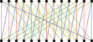
Throughout this chapter, unless stated otherwise, we will consider the PG bipartite graph made from 3-dimensional projective , as a running example. It has 15 nodes on either side (points and hyperplanes), and each node is connected to 7 nodes on other side of the graph. The hyperplane-point incidence is shown in table 1. Each row of the table lists the points that are incident on the correspondingly labeled hyperplane. The incidence relations have been calculated by constructing the Galois extension field, as outlined and exemplified in appendix A. A corresponding bipartite graph is shown in Fig. 7.
| Hyperplane no. | List of Points |
|---|---|
| 0 | {0, 1, 2, 4, 5, 8, 10} |
| 1 | {1, 2, 3, 5, 6, 9, 11} |
| 2 | {2, 3, 4, 6, 7, 10, 12} |
| 3 | {3, 4, 5, 7, 8, 11, 13} |
| 4 | {4, 5, 6, 8, 9, 12, 14} |
| 5 | {5, 6, 7, 9, 10, 13, 0} |
| 6 | {6, 7, 8, 10, 11, 14, 1} |
| 7 | {7, 8, 9, 11, 12, 0, 2} |
| 8 | {8, 9, 10, 12, 13, 1, 3} |
| 9 | {9, 10, 11, 13, 14, 2, 4} |
| 10 | { 10, 11, 12, 14, 0, 3, 5} |
| 11 | { 11, 12, 13, 0, 1, 4, 6} |
| 12 | { 12, 13, 14, 1, 2, 5, 7} |
| 13 | { 13, 14, 0, 2, 3, 6, 8} |
| 14 | { 14, 0, 1, 3, 4, 7, 9} |
To again recall from 1, logical processing unit (LPU) is defined as the logical computational unit associated with each node of the graph, while physical processing unit (PPU) as the physical computational unit associated with each node of the graph. The equivalent term for overlaid memory unit is physical memory unit (PMU), which is an overlay of multiple logical memory units (LMUs).
7.1 System Architecture and Data Flow
As discussed earlier in section 3, a PG bipartite graph represents a data flow graph, with each side of the bipartite graph representing multiple instances of one type of computation. These two types of component computations happen one after the other in flooding scheduling. To design such a system, we first refine the PG bipartite graph into an architecture diagram at the second level of refinement. At this computation refinement level, we turn the specification into a high-level architecture. For this, first the value of fold factor, q, is chosen. Recall that first level of refinement is optional. Hence in such architectural model, there are two sets of J/q PPUs, and two sets of J/q PMUs. One set of PMUs is collocated with one set of PPUs, and similarly the remaining two. One-to-one mapped local channels are added between 2 ports of each PPU, and the 2 ports of collocated PMU. Thus the read/write access between each PPU, PMU pair is local. Based on requirements imposed by the application, one set of collocated PPU, PMU pair uniquely corresponds to a subset of overlaid hyperplane nodes, and similarly the other set of collocated PPU, PMU pair uniquely corresponds to a subset of overlaid point nodes. Based on such roles, two sets of connections derived from folded PG bipartite graph, in form of channels, are added between set of PMUs of one side, set of PPUs of the other side, for both the sides. A folded architecture, which arises from such second level refinement of PG bipartite graph, is depicted in figure 8. This model qualifies to be a transaction-level model, as defined in [6].
The model of each PPU after this refinement is an untimed model that describes its internal computation in some chosen model of computation, after modifications that relate to overlaying of such units. This model cannot be a cycle-accurate model, since specification of that requires the knowledge of sequence in which inputs arrive. This sequence is dependent on design option chosen as in section 7.2.2, something that is part of next level of refinement. Hence the cycle-level details of this modification are detailed later in section 7.2.5, as part of third level of refinement. Similarly, the model of PMU after this refinement is a partially complete model, which includes a properly-sized RAM and a placeholder for an address generation component. Details of this component are filled at fourth level of refinement, as per section 7.4.4. The internal layout of these PMUs is described in section 7.4.3.
For normal (non-folded) flooding scheduling of such computation, we assume the convention that first set of PPUs read the required data from PMUs of the other side, utilizing the services of a PG interconnect. They then write the output data in their local PMU. For the next half of computation, the second set of PPUs now access the PMUs of the first type via the interconnect, to read in their data (output by the first set of PPUs). They also write back their output in their local PMUs, to be later read in by the first set of PPUs in the next iteration.
Such high-level system architecture next needs to be completed with details of further componentization (e.g., separating address generation unit from actual storage in PMU), thus taking it to last two refinement levels. This folding design is explained over next few sections.
7.1.1 Handling Prime Number of Computational Nodes
For some values of p and s, the number of nodes on one side of bipartite graph, = , may be a prime number. For such number, no factor exists, based on which second level of refinement can be carried out. To still design for folding, we proceed as follows. Since this step is not always needed, a reader may skip this subsection in first reading. We add a small number of dummy nodes to the graph towards one end of the graph, on both sides. The number of additional nodes can be at least one (in which case, the total number of nodes becomes an even number). We then convert the original circulant bipartite graph into a expanded circulant bipartite graph, using algorithm 1 described next. If the new graph is not kept circulant, then scheduling across folds will entail changing of wiring at runtime, something that is undesirable. This is because theorem 1 holds only for circulant graphs. The remaining steps in the folding design, after this optional expansion, remain identical.
In the following algorithm, if we add dummy nodes to the graph, then we also add at maximum dummy edges per retained node. All the edges retained from earlier graph are called real edges; and all that are newly added as per algorithm will be called dummy edges hereafter. The essence of the algorithm is to grow a union of perfect matchings into a union of at maximum () perfect matchings as follows. A perfect access sequence is simply the disjoint union of various perfect matchings in a balanced bipartite graph; see [24]. Let nodes on one side of the original graph be denoted as , , , , and nodes on other side as , , , . By abuse of notation, we will use the notation to not only mean a node label, but also the node index/number (). Let the end points of edges incident on extremal node on one side, , be numbered as { : }, where are indices sorted in increasing order. For each edge (fixed ‘i’) in this set of edges of extremal node, , there already exist a shift-replicated real edge , and its further shift replicas, in the original (unexpanded) graph. However, in general for various numbers , J and (non-zero) , and fixed ‘i’,
In the above equation, the left hand side tries to coincide a (-times circulantly shifted replica of edge in the expanded (bigger) graph, with the existing edge , the right hand side, which is not possible in general. Hence, in the expanded graph, where dummy nodes have been added on either side of graph, the original, real edge is no more a shift replica of another real edge . In fact, it may not be shift replica of any original edge of , .
| (1) |
The shift-replication does hold in certain cases, in which case the above equation becomes an equality. Let us define as . In the original graph, the real edge is a shift-replica of edge of , . Then, whenever = for some k (may not be i), the former real edge continues to be shift-replica of some earlier edge. For example, let be equal to (k = - 1). It is easy to see that is still a ()-times shift-replicated copy of , in the extended graph. Otherwise, in general, the equivalence class of edges within a perfect matching in context of earlier, smaller graph now breaks down into at maximum two equivalence classes. One equivalence class now contains the real edge (for fixed ‘i’) , and their shift-replicas in the bigger graph. The other equivalence class, if needed, contains another real edge (again, for fixed ‘i’) , and their shift-replicas in the bigger graph. Hence each node has upto (dummy+real) edges incident on them, due to regularity of degree in the graph.
After partitioning each perfect matching, we grow each maximal matching into a perfect matching of the extended graph by adding dummy edges, which are shift replica of this class of edges. This leads to a graph, which is circulant, but its node degree is at maximum (). An example usage of such algorithm is depicted in figure 9b, and summarized in algorithm 1. In this figure, a order-5 bipartite graph (figure 9a) is grown into order-6 bipartite circulant graph. One can see that in the bigger graph, edge is not a shift replica of any earlier existing edges, , , , as per equation 1. Hence we grow these edges separately to get two different extended perfect matchings. While executing line (9) of above algorithm, we add the shift-replicated edges.
-
•
Dummy edge as shift replica of real edge .
-
•
Dummy edges , as shift-replicas of real edge .
-
•
Dummy edges , , , as shift-replicas of real edge .
Similarly, while executing line (17) of the algorithm, we add the following shift-replicated edges.
-
•
Dummy edges , , as shift-replicas of real edge .
-
•
Dummy edges , , , , as shift-replicas of real edge .
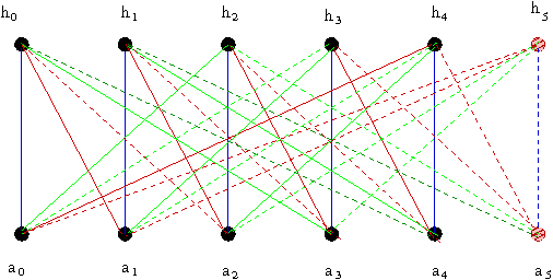
A matrix version of above algorithm is described in 7.1.2. It is easy to see that the overall graph is circulant with node degree 5, as expected (. Also easy to see is that this algorithm results in a bigger circulant bipartite balanced graph, which has additional dummy nodes on either side, and an at maximum additional dummy edges per real node. All the edges added to the additional nodes are considered dummy edges, since we do not intend to schedule any real computation on the additional (dummy) node.
We now partition such a circulant graph and schedule the folding in the standard way, as described in this paper. Whenever some dummy edges incident on any node are scheduled for input/output, they result in dummy (no read/write) event. Theorem 1 holds, and the connection remains static across folds, thus saving all the interconnect reconfiguration time. This trades off with increase in the span of the schedule, which is governed by the number of perfect access patterns within the perfect sequence. In worst case, the number of perfect access patterns, governed by (), grows by a factor upto 2. However, since we expect only small number of dummy nodes to be added, the porosity of such schedule (no transmission/reception of data on some edges in a particular machine cycle) will be less. One can immediately see that only when last fold is scheduled for computation, some of the PPUs are idle during entire computation cycle of this fold. Also, in the same fold, few PMUs do not have any i/o scheduled at some of its ports, in particular cycles. Hence some of the full (unfolded) perfect access patterns are unbalanced in the last fold. For higher folding factors q, such small imbalance is an acceptable part of our design methodology.
7.1.2 Expanding a Circulant Matrix
A circulant bipartite graph can also be represented in matrix from, via the adjacency relation. The node indices of either side of bipartite graph form the row and column indices of the matrix, respectively. If an edge exists between two nodes, a 1 is present in corresponding place in the matrix (0 otherwise). A circulant matrix representation of bipartite graph of figure 2, is shown in figure 10a.
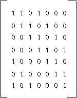
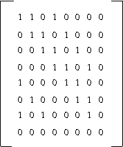
One can see that in this matrix, if there is a ‘1’ in position , then there is a ‘1’ again in position (circulance property). If we add a row and a column having all ‘0’s (equivalent of expanding the graph by = 1), the above property is no more valid; see figure 10b. Hence we need to overwrite some ‘0’s with ‘1’s in certain places, so that the above property holds again.
From figure figure 10b, we see two sets of locations where the circulance property is violated. For each ‘1’ in last column of original matrix ( = 1), we find that certain for are all ‘0’. We change such ‘0’s to ‘1’s, as shown in red font in figure 10c. Similarly, for each ‘1’ in first column of original matrix( = 1), we find that certain for are all ‘0’. We change such ‘0’s to ‘1’s, as shown in blue font in figure 10c. This way, we complete all the principal and non-principal diagonals having all values of ‘1’. It is easy to show that this algorithm corresponds step-by-step to algorithm 1.
7.2 Detailing Communication Architecture
At the next, third level of refinement, we refine the communication subsystem in the high-level architecture evolved in the previous refinement. For this purpose, we expand each edge in Figure 8, and introduce two sets of 2-to-, and -to-2 switches, and appropriate wiring between them. The value of is typically (see corollary 2 for definition of ). Design details of these switches is discussed in section 7.2.1. The wiring is governed by the generation of folded perfect access sequence generation, discussed in section 7.2.2. The exact implementation of wiring can be guided by details in section 7.2.4. At this level, the structural model of the intended system is complete, and models for many intervals in its overall cycle-accurate behavior are also available. This makes the system model at this level approximately-timed, as defined in [6]. The next (fourth) level of refinement details and integrates such intervals, and completes the entire cycle-accurate schedule, and emitting the RTL model thereafter.
The top level of complete structure of the system is shown in figure 11. To avoid congestion in the diagram, the figure shows only one of the two instances of the global, PG-based interconnect between one of the two paired, complementary sets 333The set of 2-to- switches on one side, and the set of -to-2 switches on other side form a pair of these switches. This diagram is evolved for the example system having 30 nodes, which was introduced as a running example for entire section 7, and for the fold factor discussed in subsection 7.2.3. The set of (5) edges having the same color reflect the fact that they are used in communication in a synchronous way. That is, in certain cycles, each of all the edges/wires of a particular color (e.g., yellow), between two specific ports of a pair of complementary switches carry data signals. The specific connection details (which ports, which switches) are discussed in section 7.2.2.
7.2.1 The Structure of Switches
2-to- switches are used to interface the two transmitting/output ports of each PMU, and the possible recipient/input ports of PPUs; see corollary 2. Similarly, -to-2 switches are used to interface the two receiving/input ports of each PPU, and the possible transmitting/output ports of PMUs. There are two sets of such 2-to- and -to-2 switches, since there are two sets of PPUs/PMUs in the high-level architecture. Regrouping these sets, there are two paired, complementary sets of switches, where each paired set consists of one out of two sets of 2-to- switches belonging to one side, and one out of two sets of -to-2 switches belonging to other side of the bipartite graph. Each such paired, complementary set of switches is interconnected using an instance of folded PG-based interconnect, as per section 7.2.4. The selection bits for all of each type of switch, in each of the two sets, in every relevant cycle, are synchronized and governed by calculations in sections 7.4.1 and 7.4.2.
Mostly is equal to ( = ), but sometimes . For details, the reader can skip to section 7.2.4. In brief, for each perfect access pattern whose folding results in two node indices getting re-mapped to same overlaid index, = as per section 7.2.4, one additional input/output port gets added to each switch within the paired, complementary set of switches to which the perfect pattern belongs. This tantamounts to = + , where is the number of perfect patterns for which = . Each perfect access pattern implies concurrent communication of two signals. The additional port per such pattern is needed in the above case because two, rather than one, wires are needed to concurrently support communication of two input signals between every pair of matched 2-to- and -to-2 switch corresponding to the folded perfect access pattern; again see section 7.2.4.
As pointed out in section 7.1, one type of PPUs are mapped to hyperplanes, and other type to points of a PG bipartite graph. Correspondingly, when data is being read from PMUs collocated with one type of PPUs, by the other type of PPUs, then the 2-to- switch, locally placed with PMUs, automatically assume the role of the PMU itself (point or hyperplane). Similarly, -to-2 switch, locally placed with PPUs, automatically assume the role of the PPU itself (hyperplane or point).
Each switch can be implemented by putting its port selection schedule in a LUT, and driving a multiplexer/ demultiplexer from this LUT in appropriate cycles. The schedule of one switch can be put in one LUT, and schedule of all other switches of same type in the same set can be derived using circulance property discussed in section 7.4.1. The detailed scheduling of switches is discussed as part of next level of refinement, in section 7.5.
7.2.2 Folded Perfect Access Sequence Generation
The generation of folded perfect access sequence is one of the most important step towards defining the overall schedule for system execution. This step leads to creation, rather than refinement, of a model of control flow at the third level of refinement, since the required controls of datapath elements are absent from system model so far. Thus, this model provides an abstract view of communication scheduling. Generation of schedule is governed by the details of the proof of theorem 1, which in turn deals with folding of a perfect access sequence. The model also provides inputs about wiring: which 2-to- switch to be wired to which -to-2 switch, and between which two ports of such two switches. These details will be brought out in later sections. From our design experience, this abstract schedule is the most important input to the overall design process.
By using folded perfect access sequences, we can perform parallel computation of individual nodes (PPUs) on one side of graph, in a multi-cycle synchronous fashion as follows. As per our assumption about nature of computation in section 3, we assume that the node computations use only one occurrence of each input signal.
Whenever is odd, then number of input/output per computation, , is divisible by 2. Else, when p = 2, we add a dummy edge to each node of one side in a circulant way, with the edge ending in any node on the other side. When physically scheduled, the communication over this edge, a dummy read/write, results in no transaction. Hence adding any scheduling of such edges at various points of time in a balanced schedule leads to a balanced schedule only. Physically, we propose that individual nodes are designed to ignore such dummy input value available at one of their ports, in the appropriate cycle, to avoid miscomputation. After such addition, the new number of input/output per computation is now divisible by 2. By taking, for example, two inputs at a time for computation, we can periodically schedule a binary operation on each PPU, in every few cycles (a sequential computation may take more than one cycle). The set of two edges representing the i/o for each node’s current computation are chosen so that the edge-pairs are shift replicas of one-another; see figure 6. In [14], Karmarkar showed that such 2-at-a-time processing indeed leads to perfect access pattern generation. By folding the number of nodes, and scheduling as per theorem 1, we get folded perfect access patterns for the folded architecture as well. Any sequence of such folded perfect access patterns qualifies to be a folded perfect access sequence. The algorithm for generation of folded sequence is summarized in algorithm 2.
There is thus a three-level symmetry in computation scheduling that we evolve. While exciting 2 inputs at a time, each group of J/q PPUs belonging to one fold shows memory access balance within a single cycle. Across q such cycles, all the q groups show balance. These balanced patterns from these q cycles combine to form a perfect pattern, when combined temporally. Finally, all such (combined) perfect patterns should form a balanced perfect sequence. The execution of perfect sequence, thus, takes multiple cycles.
An important 2-way design option for folded architectures is as follows. There are two ways by which we can combine the 2-input computations done by nodes of a fold. We may first schedule 2-input computations to be done by each of the J nodes across all the q folds sequentially, and then we combine partial all such partial schedules into full/unfolded perfect access patterns. Alternatively, we may first sequentially schedule all 2-input computations done by each of the J/q nodes in one fold only, and then repeat this schedule for all remaining (q-1) folds, and finally combine such patterns. The choice of this is left to the implementer. For deciding schedules of various components, we will use first design option hereafter, unless stated otherwise.
7.2.3 Example Folding and Abstract Schedule Generation
Any sequence of perfect access patterns computed in section 7.2.2 gives rise to an abstract version of computation and communication schedule. We describe this abstract schedule by folding the example graph of table 1.
For that graph, we can fold the 15 nodes on each side by a factor of 3, so that each fold/partition has 5 nodes of either type. Running the algorithm 2, we get the schedule as in table 2. The 15 LPUs are been referred as PUs, 5 physically used PPUs as PUs, and 5 physically used PMUs as MUs. A dummy MU is used as a placeholder in last perfect access pattern for the no memory transaction that is to be scheduled on 2nd port of a PU.
| Cycle # | Folded Pattern | |||||
| Full Perfect Access Pattern 0 | ||||||
| 0 | [PU0 : MU0, MU1 ] | [PU1 : MU1, MU2 ] | [PU2 : MU2, MU3 ] | [PU3 : MU3, MU4 ] | [PU4 : MU4, MU0 ] | Scheduling , edge of 0,1,2,3,4 PUs |
| 1 | [PU0 : MU0, MU1 ] | [PU1 : MU1, MU2 ] | [PU2 : MU2, MU3 ] | [PU3 : MU3, MU4 ] | [PU4 : MU4, MU0 ] | Scheduling , edge of 5,6,7,8,9 PUs |
| 2 | [PU0 : MU0, MU1 ] | [PU1 : MU1, MU2 ] | [PU2 : MU2, MU3 ] | [PU3 : MU3, MU4 ] | [PU4 : MU4, MU0 ] | Scheduling , edge of 10,11,12,13,14 PUs |
| Full Perfect Access Pattern 1 | ||||||
| 3 | [PU0 : MU2, MU4 ] | [PU1 : MU3, MU0 ] | [PU2 : MU4, MU1 ] | [PU3 : MU0, MU2 ] | [PU4 : MU1, MU3 ] | Scheduling , edge of 0,1,2,3,4 PUs |
| 4 | [PU0 : MU2, MU4 ] | [PU1 : MU3, MU0 ] | [PU2 : MU4, MU1 ] | [PU3 : MU0, MU2 ] | [PU4 : MU1, MU3 ] | Scheduling , edge of 5,6,7,8,9 PUs |
| 5 | [PU0 : MU2, MU4 ] | [PU1 : MU3, MU0 ] | [PU2 : MU4, MU1 ] | [PU3 : MU0, MU2 ] | [PU4 : MU1, MU3 ] | Scheduling , edge of 10,11,12,13,14 PUs |
| Full Perfect Access Pattern 2 | ||||||
| 6 | [PU0 : MU0, MU3 ] | [PU1 : MU1, MU4 ] | [PU2 : MU2, MU0 ] | [PU3 : MU3, MU1 ] | [PU4 : MU4, MU2 ] | Scheduling , edge of 0,1,2,3,4 PUs |
| 7 | [PU0 : MU0, MU3 ] | [PU1 : MU1, MU4 ] | [PU2 : MU2, MU0 ] | [PU3 : MU3, MU1 ] | [PU4 : MU4, MU2 ] | Scheduling , edge of 5,6,7,8,9 PUs |
| 8 | [PU0 : MU0, MU3 ] | [PU1 : MU1, MU4 ] | [PU2 : MU2, MU0 ] | [PU3 : MU3, MU1 ] | [PU4 : MU4, MU2 ] | Scheduling , edge of 10,11,12,13,14 PUs |
| Full Perfect Access Pattern 3 | ||||||
| 9 | [PU0 : MU0, D ] | [PU1 : MU1, D ] | [PU2 : MU2, D ] | [PU3 : MU3, D ] | [PU4 : MU4, D ] | Scheduling edge of 0,1,2,3,4 PUs |
| 10 | [PU0 : MU0, D ] | [PU1 : MU1, D ] | [PU2 : MU2, D ] | [PU3 : MU3, D ] | [PU4 : MU4, D ] | Scheduling edge of 5,6,7,8,9 PUs |
| 11 | [PU0 : MU0, D ] | [PU1 : MU1, D ] | [PU2 : MU2, D ] | [PU3 : MU3, D ] | [PU4 : MU4, D ] | Scheduling edge of 10,11,12,13,14 PUs |
The schedule of PUs in each fold per clock cycle can be easily seen to be balanced. Put together, they first form a full perfect access pattern every 3 cycles, and then perfect access sequence in 12 cycles.
7.2.4 Wiring the Interconnect
As mentioned earlier, wiring is assumed to be direct in our case. By theorem 3, it is possible to fold in such a way that certain (overlaid) nodes always access same set of out of J/q PMUs. Hence the connections remain static, as the computation schedule moves from one fold to another. This is one of the most significant advantages of folded PG bipartite graphs. Each wire connects one port of a 2-to- switch, and one port of a -to-2 switch, as already discussed in section 7.2.1. This static-ness is easily illustrated using the example folding shown in table 2, by picking any column and each set of 3 continuous rows under some full perfect access pattern.
Referring to section 6.1, if the end points of two connections of a particular node being considered in a particular cycle, in a folded graph are equal (e.g. = ), the number of wires to each PMU from each reachable PPU become double. It requires double channel width, which trades off with decrease in the switch size. Also, wiring two interconnects between same pair of source and destination nodes may possibly lead to subsequent wiring/routing congestion at later design flow stages. One can then alternatively try to design for another folding factor. Since our methodology accepts any q that is a factor of J, we can vary q and may get a design for which .
7.2.5 Relating Communication Refinement to Modification in Microarchitecture of PPUs
The fundamental problem of overlaying of datapath elements needs to be handled in all possible folding designs. This design step naturally fits in the second level of refinement, which deals with computational refinement. Hence it has been handled via creation of the untimed model. However, timing of this model depends on order of input arrival, i.e. the choice of a design option discussed in section 7.2.2. Hence this part of micro-architecture evolution is made part of third level of refinement.
Especially in case of operators, within PPUs, that consult all input data to a node(’s computation), some changes are needed to save state, including the intermediate results. For example, let each node’s computation have an accumulation(/max/min) operator present within. In the schedule of first folding design option, accumulation is only done partially for each node that is overlaid on the PPU, across multiple folds during one run of a perfect access pattern per fold. The current partial sum needs to be stored separately for each fold, since in the next run of perfect access pattern in the sequence for the same fold multiple cycles later, this partial sum needs to be carried over. Hence per PPU, copies of each register holding such intermediate result need to be created.
In the second design option, any register along the datapath of PPU, whose contents are read and used later on after multiple cycles, needs to again have copies each. This is because in this interval, overlay of such register would have happened. Of course, switches to select the right register copy in a particular cycle, driven by the fold index currently in operation, also need to be inserted in the datapath for this design option.
7.3 Issues in Overall Scheduling and Design Completion
The control path of a synchronous VLSI system is implemented using a cycle-level schedule. All aspects of folding being dealt in the current section 7 pertain to folding the data path of a suitable system, by doing stepwise refinement of the corresponding DFG. The control path can be evolved alongside, from the original schedule of an unfolded VLSI system. In the schedule of such system, there will be intervals, in which datapath elements will be re-used. By interval, we imply some contiguous sequence of machine cycles. Such intervals need to be expanded by a factor, along with insertion of new control signals which define e.g. the fold index currently in operation. Expanding generally implies replicating an interval in which a certain control signal is TRUE, q times in a contiguous way. Memory access interval, node computation interval, switch enable intervals etc. all need to be expanded by a factor. It is possible to identify and enlist such intervals at RTL level model of the datapath. Automating the generation of new, expanded schedule using this list, especially when control path is implemented using microcode sequencing, is straightforward.
However, some of these expansions can be best worked out from scratch, rather than working with an interval of schedule for the unfolded system. This is because in some places, rather than interval of one signal, interval of a set of related signals gets expanded by factor q. Further, in such groups, the order in which signals were earlier turned TRUE gets rearranged. For example, group of switch selection signals show this characteristic due to folding. Hence it was pointed out earlier that after the third level of refinement, intervals in the cycle-accurate behavior of the intended system, some reflecting folding and others not reflecting folding, are also available. For such intervals, the schedule generator must focus on inserting/replacing appropriate schedule intervals, rather than expanding. To generate such replacement intervals, the schedule derived in section 7.2.3 is used as base schedule to derive individual schedules (cycle-accurate behaviors). To summarize, it is the fourth level of refinement that expands/inserts and integrates these intervals, completing the implementation of entire control path of the system via a cycle-accurate schedule (system behavior), and emitting the RTL model thereafter.
Though this schedule governs the behavior of individual components, certain auxiliary details such as selection order of ports of some switches, which is needed for schedule derivation, also need to be now specified. We cover all these detailed auxiliary issues, and the overall schedule derivation, in remaining part of section 7. Before going into details, we first summarize all the remaining issues that need to be tackled. Generating details corresponding to solution of these issues is the other concern of the fourth level of refinement.
A schedule for the parallel computational model discussed in section 3 needs to address issues in two identical computation phases, due to flooding nature of the computation algorithm. Correspondingly, as shown in section 7.1, there is a pair of PPU, PMU relations. One relation relates PPUs of left side of bipartite graph to PMUs on right side of bipartite graph, from which they read the input data in parallel. Similarly, the other relation relates PPUs of right side of bipartite graph to PMUs on left side of bipartite graph, from which they read the input data in parallel. The two reading phases, though identical, are disjoint. Hence we can simply solve the issues in communication schedule derivation for one relation only, and apply the answers to the other.
We identify the following issues in generating the communication schedule.
7.3.1 Issues for Physical Processing Units
For a full (non-folded) perfect access pattern, after folding, we note the following issues.
-
1.
Each LPU, when scheduled over an overlaid PPU, reads two data items from two of its edges in a particular machine cycle. How to know which two edges are being active?
-
2.
The one out of (J/q) PPUs of fold accesses one or both its data in PMU for the perfect access pattern (see theorem 1). How to get the value of p?
-
3.
How to decide whether one or both the data are going to be stored/read in the same PMU?
-
4.
Given the index of PMU, from which locations will one/both of the data items be read during full perfect access pattern?
The last issue actually pertains to address generation for the read data. Hence we address this issue as part of the issues in PMU scheduling itself, in the next section.
Since after computation, PPUs write the result in their local memory, there are no folding-related issues in write-back. This is data is to later read by PPUs of the opposite side, using the edge/connection that connects the PPU and the PMU. Two issues for a PPU, while writing back data corresponding to an edge, are:
-
5.
After computation, at which location of local memory must each PPU write the data corresponding to an edge?
-
6.
At each location, in which machine cycle must each PPU write the corresponding data?
7.3.2 Issues for Physical Memory Units
The PMUs are also involved in distributing read data in parallel to various PPUs. The reading of data is in bursts, and it happens in certain successive cycles that make up the entire perfect access sequence. Correspondingly, read addresses need to be generated somewhere in the system, which are used by PMUs to provide data in various machine cycles.
For a full (non-folded) perfect access pattern, after folding, we note the following issues.
-
1.
To which PPUs must a PMU send out data?
This question is a dual question of issue for PPUs, and can be easily solved for by inverting the map generated for that problem. Hence we leave out reporting detailed solution to this issue.
-
2.
In a given cycle, a PMU must send out data from which location, to which PPU?
Because this issue is dealt by generating corresponding address, we transform this question into following address generation issue. If the PPU working on some binary operation (read-)accesses the PMU, then in which cycle does it access it, and at which location (local address)? Here, is defined as the node of the unfolded graph, whose location on one side of the bipartite graph is extremal w.r.t. other connected nodes to PMU. Answering this question, and then extending the schedule using the sequence generation implicit in section 7.2.2, the entire addressing can in fact be evolved.
Another set of issues arise, when addresses need to be generated for local memory during the write-back phase of a PPU. In this phase, the PMU is fixed: it is the local memory. However, the location in which a datum must be written in each cycle varies. It is easy to notice that this issue is addressed by the last two (address generation) issues in section 7.3.1. The order in which PPUs of other side/type will access datum for input dictates the order in which data must be stored into these local memories. The read/write address generation issues will hence be address jointly later.
Throughout remaining section, we continue to assume the natural left-to-right labeling of vertices on either side of the graph, as shown in figure 6.
7.4 Solutions to Auxiliary Issues
The detailed solutions to above issues are discussed in this section. A reader may choose to skip over to next section 7.5 during initial reading.
7.4.1 Edges used in a Perfect Access Pattern
In this section, we address the issue raised in section 7.3.1. To summarize, this issue relates to finding out which two edges of each node of the folded graph will be used for reading data in a particular cycle. Recall from section 7.2 that 2-to- switches are interfaced with output ports of various MUs. Addressing issue is important to synchronize the port selection logic of all 2-to- switches, that are interfaced to PMUs of each type. This is because the switches address their lines in a local way, i.e. labeling of their output ports is local. One has to then provide an explicit mapping so that the local indices of lines selected by e.g. 2-to- demultiplexer switches, present at the output of each PMU, form an (unfolded) perfect access pattern. It also completes the behavioral specification of 2-to- demultiplexer switches.
PMUs are themselves responsible for generating the port selection bits, to be used in various perfect access patterns. Partitioning the edge set into subsets of two, and sequencing of these subsets, for each set of two folded PG interconnects, as defined in section 7.2.2, is needed to define these patterns within a perfect access sequence for each of these sets. The address generation has been covered in detail in section 7.4.4 later. The interconnect connects either hyperplane nodes to point nodes, or point nodes to hyperplane nodes, depending which of the two folded PG interconnects we are working with. Correspondingly, the synchronized scheduling of ports of 2-to- switch is based on partitioning either the sorted point set of the hyperplane (index) corresponding to the switch, or the hyperplane set of the point (index) corresponding to the switch, whichever is the role of the switch (also see table 2). Either way, each PPU receives two data input on two edges. Given a PMU (and a local 2-to- switch) with index m, we consider the left-extremal node (corresponding to a -to-2 switch) connected to it in the unfolded graph, . Here, extremality implies that the location of on one side of the unfolded bipartite graph is in left extreme w.r.t. other connected nodes to PMU. For example, in figure 2, node p2 is extremally connected to node l1. Further, let the totally ordered point set of be denoted as {, , , }, where . Let us also impose an order on the edges of , so that we define the data of to be the edge between and .
However, while the data of is leftmost or rightmost edge of , it may not correspond to the leftmost or rightmost edge for , due to circulant rotation applied on the edges. Here, finding leftmost or rightmost edge of a node corresponds to sorting the destination nodes of various edges incident on the source node, in increasing order, and taking the element of sequence and its corresponding edge, exactly as discussed in previous paragraph. Hence we need to have a way, which given an edge, provides which all edges are circulant shift-replicas of it. We give the details of such circulant edge mapping now.
Recall that {, , , : } (ordered point set). Hence m is equal to for some t. Let us take another arbitrary node , which may or may not be connected to the PMU m. Without loss of generality, let ( – ) = , where the difference is taken modulo-J, and hence is always positive. Then, due to circulance, the point set of can be represented as {, , , }. The addition here is again modulo-(J) addition. Because of modulo addition, the total order , , , gets shifted in a circular way over the modulo ‘ring’. If we sort this set of indices in increasing order, then { ( = ), ( = ), , ( = )}, must be equivalent to for some x. It can easily be verified now that if the edge between m and was edge of , then the corresponding shift-replicated edge incident on is an edge between and . This edge need not be the element of the sequence .
As an example, we take the graph of table 1. Let m be point, i.e. p6. From the table, its left-extremal neighboring hyperplane is h1. Let r = 4, in which case the edge of h1 connects h1 and p5 (not p6). Let = , in which case = 11. In terms of total order, the left-to-right edge of ends on p7, but this edge is not a shift-replica of the edge . Rather, the edge of , which should be a shift-replica of edge of , runs between and = . Looking at the table, we find that this is indeed true.
An LUT can be used to store this edge-selection schedule. A simple way of generating the edge-correspondence is to start by choosing an m such that has a label of 0. Defining an order on edges on node is then natural, straightforward left-to-right labeling.
For some designs, in the last perfect access pattern, a dummy edge is scheduled, to allow a PPU to read from a dummy PMU, a no value. To implement this, selection of dummy MU for input to a 2-to- switch is done by using an invalid value of selection signal, so that all but one output of 2-to- switch remain tristated, thus achieving the effect of no value read on one port.
7.4.2 Pairing PPUs with PMUs
In this section, we address and issues raised in section 7.3.1. To summarize, the former issue relates to finding the PMUs to be contacted while execution of a particular full perfect access pattern, while the latter issue relates to knowing if both the data are to be read from single PMU. Like in previous section, addressing these issues is important to synchronize the port selection logic of all -to-2 switches that are collocated with PPUs of each type, for each perfect pattern within the sequence evolved in section 7.2.2. Hence, hereafter we will address the issue of synchronizing -to-2 switches for any perfect access pattern, by using a variable index. Like 2-to- switches, these switches also address their lines in a local way, i.e. labeling of their input ports is local. One has to then provide an explicit mapping so that the local indices of lines selected by e.g. -to-2 multiplexer switches, present at the input of each PPU, form the same folded perfect access pattern, that the PMUs of other type use for communication, as per previous section 7.4.1. Since the two chosen ports of all 2-to- switches of are synchronized, it is necessary to ensure that the set of destination ports of wires stimulated during execution of a particular perfect access pattern, and having source ports in the 2-to- switches, are specifically assigned based on the synchronized choice of two ports made on all of the -to-2 switches. Only that way, the signal driven on a wire by e.g. 2-to- switch, will pass through a selected port of -to-2 switch in next cycle, towards the destined PPU. Yet again, making such selections for all patterns in a communication sequence also completes the behavioral specification of -to-2 multiplexer switches.
Overall, the synchronized scheduling of ports of -to-2 switches for entire perfect access sequence is done by using schedule reciprocal to that of schedule of ports of 2-to- switches. In an unfolded design, it is easy to prove that this can be obtained by doing same partitioning of hyperplane/point set corresponding to each -to-2 switch, but by inverting the sorted order of the set first. However, it is not straightforward in a folded design to get the inverse schedule in such easy way. Hence we derive the inversion by first principles as follows.
To know the contacted PMUs by a PPU, as enabled by the contact of various -to-2 switches with corresponding 2-to- switch, we first try to calculate the value of p, where one out of (J/q) PPUs of fold accesses one or both its data in PMU for perfect access pattern. Here, perfect access pattern is defined as one that executes and edges of PMU; see section 7.4.1 (and table 2 for an example).
We use the non-folded regular bipartite graph to answer this. We also use the correlation between edges belonging to same perfect access pattern, brought out in previous section 7.4.1. Given a PMU index m and the extremal node connected to it in the unfolded graph, , let its totally ordered point set be denoted as {, , , }, where . For the = node in the unfolded graph, let ( – ) = , where the difference is taken modulo-J. Due to circulance, the point set of can be represented as {, , , }. The addition here is again modulo-(J) addition. It is immediately obvious that for perfect access pattern, node exercises its two connections to () and ().
Let = [() modulo-(J)] modulo-(J/q), and = [() modulo-(J)]modulo-(J/q). Then, from theorem 1, it is straightforward to see that the PMUs accessed by one out of (J/q) PPUs of fold for the perfect access pattern are found in appropriate bins of and PMUs. Table 2 is organized to explicitly exemplify such folded mappings. These PMUs are collocated with the PPUs on the other side. The algorithm of deriving the pairing is summarized in algorithm 3. One can immediately see that while the number of LMUs have decreased, the size of each PMU has increased proportionally. Hence this design is a definite case of linear folding.
Identical PMU Indices
A special case may arise when = , due to the modulo operation, for a particular full perfect access pattern. Then the data corresponding to two consecutive edges of each node of the entire non-folded graph get stored in same PMU. In that case, both the data corresponding to perfect access pattern access are found in the same PMU. The whole architecture still works, as discussed in section 6.1. This addresses the issue raised in section 7.3.1. Since both data are to be fetched concurrently in a cycle by each PPU from the same PMU in this perfect pattern, two ports per 2-to- and -to-2 switches belonging to one paired, complemented set are used between each pair of such matched (PPU to PMU mapping) switches simultaneously. As expected, the concurrent usage of such pair of ports is itself synchronized across all switches of same type, for both 2-to- and -to-2 switches within their respective sets. Since our interconnect graph is symmetric, exactly the same scheme can be used to place the data produced by PPUs of the other side.
7.4.3 Internal Layout of PMUs
Now we try to address the issue raised in section 7.3.1 (and issue of section 7.3.2 partially). To summarize, this issue relates to finding out one/both the locations within a PMU, which is read-accessed by a particular LPU w.r.t. execution of a particular full perfect pattern. In section 7.2.2, we pointed out two different ways by which we can combine the 2-input computations done by a fold. Ideally, the internal layout of each PMU may simply follow the time-order in which the edges incident on it are scheduled. In such a case, the address generation unit becomes simply a counter. We do the layout design with this as objective. The layout is briefly described only for conceptual clarity, and does not directly result in any design step. It influences the design of address generation scheme, though, and hence its value.
This internal layout depends on the design option chosen. In the following, we explain the internal layout for first design option. Deriving the layout for second design option on similar lines is straightforward.
For this option, the first level substructure arises by making ‘/2’ bins within each PMU, one bin for each of the full (non-folded, rolled out) perfect access pattern. A bin is defined as a contiguous chunk of memory within the unit. Whether for some perfect access pattern, the re-mapped indices of 2 LMUs are same or different, one can easily prove that the number of bins remains constant. The size of each bin is thus a constant as well, . Whenever , the degree of each node in bipartite graph, is odd, the last bin contains only q real data items, and q items corresponding to storage of dummy edges. Given the overall size of each PMU, this wastage is negligible. The bins are arranged in linear order with respect to full perfect access patterns. Hence the address generator simply needs to generate addresses in linear order in each cycle, whenever read needs to be performed. For write, the addressing is structured but not linear; see section 7.4.4. In the execution of a perfect access pattern, each PPU accesses two memory locations. It may access them either in same PMU, or in different PMUs.
-
•
In the former case, assume that one out of (J/q) PPUs of fold (0 i J/q, 0 k q) stores both it’s data in (some) PMU (see section 7.4.2 for calculation of p). If the index of current perfect pattern being executed is l, then these two data are in bin of PMU in two consecutive locations. The offset of these locations from start of the bin is expectedly, 2k and (2k+1).
-
•
In the latter case, assume that one out of (J/q) PPUs of fold (0 i J/q, 0 k q) stores exactly one data in (some) PMU. The possible values of p are fixed as detailed in section 7.4.2. If the index of perfect access pattern is l, then (one of the two) data is placed in bin of PMU. Since we are folding a perfect pattern, exactly two edges will have their re-mapped LMU indices as that of a particular PMU. Hence, if one out of J/q PPUs of fold also accesses PMU, and if , then the offset of location for data corresponding to PPU from start of the bin is 2k, while that of is (2k+1). This accounts for address mapping relative to circulant rotation of edges in the folded graph (see figure 6).
A color-coded version of memory layout for first design option is shown in figure 12. The parameters of graph in this figure are J=6, =6, and q=3. Hence there are J/q=2 PMUs. The set of 3 similar-colored boxes in each column, PU*, represent excitement of all the 6 edges incident on them at appropriate time, 2-at-a-time. These two edges represent the two data items consumed by each PU in a cycle. The same color has been used to depict the location of these two data items in the two PMUs. Each PMU has = 3 bins, one corresponding to each perfect access pattern. Each bin has data item placeholders. For example, the two data items used by PU3 during execution of third perfect pattern can be found in bin of both PMUs, in location relative to start of the bin, one each in both PMU. Both these placeholders have same color as of the box under PU3 for full pattern. Depending on the perfect access pattern, a particular PPU may store both its data items in same PMU, or not. This fact can easily be seen to be dependent on the two indices of destination vertices of the two edges that are being scheduled as part of that particular perfect access pattern. So, in this example, for the pattern, each PPU stores both its data items in same PMU, while it does not for remaining patterns. It can now be seen that the address generator unit is simply a counter, the topic that we cover in next section.
Because we schedule binary operations on the PPUs in each cycle, the PMUs are all dual-port memories.
Layout of Units for Local Access
The above layout of PMUs was evolved for read access required by each computing node. After computing, data corresponding to each edge is written into local PMU of the computing node. Since the same PMUs are later accessed by PPUs on the other side of bipartite graph for input data, the data written into these local units needs to be organized again in the same form, as discussed above. In fact, the address generation scheme for writing also remains same, as that of the read accesses that follow. This addresses the and issues raised in section 7.3.1. To summarize, the former issue relates to finding the location of the local memory of a particular PPU in which data corresponding to an edge has to be written into, while the latter relates to knowing the machine cycle in which writing has to be performed.
7.4.4 Address Generation
Here, we first address the refined issue raised in section 7.3.2: if the PPU working on some binary operation accesses the PMU, then in which cycle does it access it, and at which location (local address)? To simplify generation algorithm, we take as , and m as PMU connected to it, as discussed in section 7.4.1.
As such, the address generation requirements are apparent from the memory layout and flow of time, as depicted in figure 12. Since we can combine balanced patterns for a fold in two different ways to form a perfect sequence, the requirements also correspondingly differ. For illustration as well as continuation, we take the first design option again. We now calculate the schedule for edge of any node, which is shift-replica of edge of . Details of this replication were discussed in section 7.4.2 earlier.
Lemma 4.
For the first design option, the data associated with LPU is accessed from some PMU’s some location (computable from section 7.4.3) in cycle number , where T is the number of machine cycles taken for completion of computation by each node.
Proof.
Each PPU computes on behalf of q overlaid LPUs in first design option, per perfect pattern. Further, before arriving at the right (current) perfect access pattern in which data is consumed, full perfect access patterns must have completed execution. This is because by definition, perfect pattern is one that excites edge of ; see section 7.4.2. Due to overlay, LPU gets scheduled during the current perfect access pattern only in cycle number (k+1), counted from the beginning of the current perfect access pattern. These two components add up to give the cycle number required. ∎
It is straightforward to further note that the J/q circulantly shifted replicas of edge of , within the same fold, also get scheduled in the same cycle. By varying the values of t and k, we can cover schedule for all the edges of all nodes, i.e. the complete schedule. Knowing the two locations per cycle in each PMU that the schedule uses, the address generation counters of various PMUs can be synchronized. The algorithm for address generation is summarized in algorithm 4.
Continuing the example graph of table 1, let t = 5, so that the edge of ends on p5. Assuming the earlier fold factor q as 3, h0 is in first fold of the graph. Hence the edge of h0 is scheduled in = clock cycle.
We also state without proof, another address generation scheme.
Lemma 5.
Each PMU is a true dual-port memory, and hence each port requires a separate address generator. If we stick to the convention defined next, it is easy to verify that both the address generators will be a counter. Assume that the execution of next perfect access pattern needs to be scheduled at each port now. Each PPU accesses two memory locations. For the next pattern, it may access them either in same PMU, or in different units.
-
•
In the former case, exactly one PPU per fold will store both its data items of this pattern in the particular PMU. Then, in the relevant machine cycle, let the defined convention be that the first port read/write the data item at offset 2k from the beginning of the bin corresponding to this pattern. By similar convention, in the same cycle, second port reads/writes the data item at offset 2k+1 from the beginning of the bin corresponding to this pattern. Here, k is the index of the fold that is currently being scheduled.
-
•
In the latter case, exactly two PPUs per fold read/write one data item each into the PMU in question. Let the re-mapped indices of these PPUs (after folding) be and . Also, without loss of generality, let . Then, in the relevant machine cycle, let the defined convention be that the first port read/write the data item at offset 2k from the beginning of the bin corresponding to this pattern, which is exchanged with PPU . By similar convention, in the same cycle, the second port then reads/writes the data item at offset 2k+1 from the beginning of the bin corresponding to this pattern, which is exchanged with PPU .
Write Address Generation and Multiplexing
We now address the related address generation issue pointed out in section 7.3.2: in write-back phase to local memory by a PPU, in what sequence of locations must the output data generated in successive clock cycles be stored? We had hinted that the order in which PPUs of other side/type will access this generated datum as their input input, dictates the sequence of locations in the local memory.
We start by observing that in absence of folding, the data must be written in reverse (linear) order of locations into local memory. From previous section, the read order of a PMU was found to start from location, and increase in a step of 1 till the last location, which we term as forward linear order. The write order, which is reverse of this, is hence termed as reverse linear order. This is easy to prove using circulance property of the perfect matchings that form the each perfect pattern, which in turn combine to form the perfect access sequence. Take two successive edges incident on a node having index , on one side of the graph, and let and be the indices of end points of these edges (on other side of graph) such that without loss of generality. These two edges are part of two different perfect matchings. When we look at e.g. node and observe the perfect access pattern to which these two edges belong, one can see that the node contributes one of these edges incident on it, plus an edge that is part of the perfect matching to which the other edge belongs, to the (same) perfect access pattern. Let the other end of this different edge be a node having index . If , it is straightforward to prove that . Hence for read order to be forward linear, the write order must be reverse linear, in absence of folding. For the example folding of graph of table 1, one can see this order in table 3. The table tabulates the data input sequence of point nodes, as generated in certain order by various hyperplane nodes. In the table, A-O are (15) hyperplane labels, and for each hyperplane, e.g., A, A0 represents edge data, out of 8 edge datum4447 real + 1 for dummy edge for last perfect access pattern, generated by hyperplane A. Further, the numbering 0-6 has been done based on perfect access pattern-based grouping of edges, that are incident on the consumer (point) nodes. Thus, from table 1 or Fig. 7, A0 is the data that is read from hyperplane 0 by point 0, A5 is the data that is read from hyperplane 0 by point 8, and so on.
| Point Index | Sequence of Data Item Output | ||||||
|---|---|---|---|---|---|---|---|
| 0 | A0 | F6 | H5 | K4 | L3 | N2 | O1 |
| 1 | B0 | G6 | I5 | L4 | M3 | O2 | A1 |
| 2 | C0 | H6 | J5 | M4 | N3 | A2 | B1 |
| 3 | D0 | I6 | K5 | N4 | O3 | B2 | C1 |
| 4 | E0 | J6 | L5 | O4 | A3 | C2 | D1 |
| 5 | F0 | K6 | M5 | A4 | B3 | D2 | E1 |
| 6 | G0 | L6 | N5 | B4 | C3 | E2 | F1 |
| 7 | H0 | M6 | O5 | C4 | D3 | F2 | G1 |
| 8 | I0 | N6 | A5 | D4 | E3 | G2 | H1 |
| 9 | J0 | O6 | B5 | E4 | F3 | H2 | I1 |
| 10 | K0 | A6 | C5 | F4 | G3 | I2 | J1 |
| 11 | L0 | B6 | D5 | G4 | H3 | J2 | K1 |
| 12 | M0 | C6 | E5 | H4 | I3 | K2 | L1 |
| 13 | N0 | D6 | F5 | I4 | J3 | L2 | M1 |
| 14 | 00 | E6 | G5 | J4 | K3 | M2 | N1 |
In presence of folding, the write order has to factor in interleaving of data, as is done by the overlaid (point) nodes. For example, recall that hyperplanes A, F and K are overlaid, and so on. Data corresponding to edge A0 is consumed by point node 0, which belongs to first fold of point nodes (i = 1), during its execution of first perfect access pattern (j = 1). Similarly, data A4 is consumed by point node 5, which belongs to second fold of point nodes (i = 2), during its execution of second perfect access pattern (j = 2). Since A0 is to the left of F6, when looking from point node 0, as in Fig. 7, A0 is stored in ((i-1)6)+(j-1)*2+0 = ((1-1)6)+(1-1)*2+0 = location. Similarly, F6 is stored in ((i-1)6)+(j-1)*2+1 = ((1-1)6)+(1-1)*2+0 = location, and A4 in ((i-1)6)+(j-1)*2+1 = ((2-1)6)+(2-1)*2+1 = location. This way, algorithmically, the entire folded write order can be generated.
Such a write-back address sequence can generally be implemented using an LUT. A multiplexer is also generally needed to choose between read and write address generator’s outputs, to be interfaced with PMU’s address inputs, in a particular clock cycle.
Implementing the Generator
There are two ways by which PPUs can access operands stored in
PMUs in a particular cycle. In the first way, the PPUs
themselves calculate/generate and place the address/location using an extra
bus, for a memory access. This is a standard practice in
von Neumann
architectures. Since there is a deterministic structure in access order, it
is possible to do the other way round. One can alternatively build and
embed an address generator within the PMU (alongside its controller), which places two data
objects on the two ports (or alternatively, allows two data objects to be
stored at two locations), given the cycle number. For each PMU, we need one address generation unit, in either case.
7.5 Derivation of Complete Schedule
With the individual issues related to complete schedule derivation for a folded PG-based system addressed in previous section, we now describe how the entire computational schedule, without pipelining, can be arrived at. It is easy to understand this schedule by looking at the detailed structure of the system, as in figure 11. We assume that LPUs of first type take units of time, and of the second time take units of time, for their computation. A PPU is an overlay of q LPUs, and hence the two types of PPUs take and units of time to compute, respectively. The required expansion of this interval of computation, based on the design option chosen as per section 7.2.2, can be easily generated from original schedule interval of one representative out of the grouped PPUs.
After e.g. first type of PPUs finish computation, the output will need to be stored into local PMUs. There are edges per node, overlaid q times. Accounting for dummy edges whenever is odd, units of time will be taken by each PPU to write back all its output data into local PMU. The schedule for this interval is simply a counter that drives the write-back location generation logic, and hence can be easily extended by a factor of q.
After local storage, the new data will be required by the PPUs of other side. This requires participation of both 2-to- and -to-2 switches in almost lockstep fashion. More specifically, to allow the data to be read from one end from a PMU, and passed across the other end of the interconnect to a PPU, switches of both types in each of the two sets are active in same set/interval of machine cycles, except one cycle each at either end of the interval. This minimal staggering is because the system being a completely synchronous system, -to-2 switches can only be activated one cycle later, after 2-to- switches have put the data on the interconnect wires. The cycle interval in which switches in each set are active, starts at a cycle number computable from section 7.4.4, and lasts cycles. Here, T is equal to either or , depending on which PPUs require the data. The data is read, for one cycle, only every T cycles. Hence switches are periodically enabled every T cycles.
The above schedule is symmetric, and hence with appropriate change in the set of signals, can be used to derive the other half of schedule, in which other sets of PPUs, local PMUs, and 2-to- and -to-2 switches are involved.
7.5.1 Complete Schedule with Pipelining
Pipelining the above system leads to saving of clock cycles to some extent, and corresponding recovery of throughput. In a partially or fully structural model of a VLSI system that is composed of component hierarchies, pipelining can be tried out between every two components that are adjacent to each other in the data flow, and belong to same level, at every level of component hierarchy. For our intended system, pipelining can be performed at three levels. It can be tried at the graph level, by trying to pipeline computation done by one type of PPUs, with the other type of PPUs. It can also be tried at the high-level architecture level, as in figure 11, and finally at micro-architecture level, i.e. computation done by each node. In the latter case, each node can consume 2 inputs (1 at each port) every clock cycle, and hence value of T becomes 1 for the sake on periodic input consumption. In the former case, one can, for example, pipeline the write-back phase of a PPU. As soon as a PPU is ready with some data that can be output, it starts storing it in its local PMU in a pipelined fashion. A prototype design that we did using this methodology uses pipelining wherever feasible. Doing such pipelining will shrink the simple folded schedule discussed earlier. However, with appropriate guidelines, the above shrinking can also be automated. The (positive) impact of these two levels of pipelining on throughput depends on the time taken by each PPU, T, which varies across systems being modeled. Hence the improvement figure is not generalizable.
Finally, for pipelining at the graph level, the second design option discussed in section 7.2.2 opens up an avenue to do coarse-grained pipelining of the system. Recall that in this design option, we may first sequentially schedule all 2-input computations done by each PPU in one fold only, which cover up the complete computations of J/q nodes in the non-folded version. In default mode, the system scheduler waits for more rounds of such computations to cover remaining nodes of one side of the unfolded graph, and then schedules the communication of the results of entire one side computation to the PMUs belonging to the PPUs on other side of the graph. Instead, we can start communication as soon as computations over PPUs of one fold is over. In parallel, we can also start doing computation for next lot of J/q PPUs.
To characterize the impact of this level of pipelining on throughput, we assume that 2-input computations by each PPU happen in a single cycle. Further, due to dual-port memory assumption, and no write/write conflict while writing into PMUs (see section 7.4.3), one can assume that 2 data get stored in a memory unit per cycle. However, there may be additional communication latency due to e.g. passage of data through switches, before it arrives at the port of memory units. Assume this constant latency to be cycles. Then, it is easy to see that each half-iteration (input of data, computation and communication of resultant data) over all folds takes cycles optimally. This is almost a two-fold improvement over a non-pipelined design, where a half iteration would have taken cycles. The cost of can be amortized in the case of big-sized problems (higher ), as is practically always the case.
7.6 Putting it all Together: Summary of Design Methodology
We start the usage of this methodology by accepting an annotated PG bipartite graph as input specification, in which the nodes are annotated with their untimed behavior. The graph is parameterized in terms of order J and (regular) degree . If not pre-sorted, then the bi-adjacency matrix of the graph is first sorted so that the circulant symmetry inherent in PG bipartite graphs becomes explicit. If J is a prime number, we first expand the graph to non-prime order, as in section 7.1.1. The choice of number of nodes, , to be added on each side of the graph can be influenced by two factors. One is the factorizability of , and the other is whether for some value of , equation 1 becomes an equality. In such case, the expanded degree of each node is lesser. We then calculate all possible factors q of J. We finally select one of these factors based on various judgements. One of the possible reasons could be if the modulo operation of end point of two edges leads to the same index or not. Another reason could be the overall area budget (for example, as approximated using gate count). We then instantiate J/q PPUs and PMUs, as well as J/q 2-to- and -to-2 switches to interface them. This set of components correspond to one side of the bipartite graph, and hence is further duplicated to implement the other side of the bipartite graph as well. The internal micro-architecture of PPUs is then suitably modified to handle folding, as per section 7.2.5. Local interconnect is added between each of the two ports of each of the -to-2 switch, and a port of its local PPU. Local interconnect is also added between each of the two ports of each of the 2-to- switch, and a port of its local PMU. Two instances of global interconnects, one each between the 2-to- and -to-2 switches of opposite sides, are designed using guidelines in section 7.4.2. We then generate the folded perfect access patterns for communication over these global interconnect instances, as per algorithm in section 7.2.2. If any initialization data is to be provided to any type of LPUs, it is provided in a multiplexed way to the overlaid PPUs, at the beginning of the computation. Similarly, any output data from LPUs of one type is to be physically obtained by demultiplexing the output of corresponding overlaid PPUs. At this point, the control path and the timing of the system are evolved. The invocation (start) of this sequence signifies flow of data inputs for PPUs on one side of graph, from PMUs located on other side of graph. Accordingly, partial computations can be done on these PPUs, as soon as some subset of data arrives. At the end of invocation of one complete perfect sequence, one side of graph is through with its parallel computation. Another invocation of perfect sequences communicates the resultant data into the local memory of PPUs on other side of the graph. These PPUs can then again start acting immediately on this recent data. If the computation is iterative, the same sequence repeats. The address generation of various PMUs, (whose layout is described in section 7.4.3) whenever a perfect sequence is active, is governed by the algorithm in section 7.4.4. The generation of selection signals for various switches (described in section 7.2.1) is governed by derivations in section 7.4.1 and 7.4.2. The derivation of overall schedule is finally done, as discussed in section 7.5.
8 Models, Refinement and Design Space Exploration
As introduced so far in this paper, we use five successive levels of abstraction for models, and correspondingly four refinements in our methodology. We now show the correspondence of this methodology to general synthesis-based communication architecture design methodologies, both generic and specific. Such correspondence was found out post-specification of this methodology, reinforcing our belief that practical, useful design flows can be implemented for this methodology.
8.1 Model Abstraction Levels in Generic SoC Design
In generic SoC design, following models are used at various levels of abstraction [21], [7].
- Functional Model
-
is generally a task/process graph model, capturing just the functionality of the system.
- Architecture-level Model
-
is created by refinement of functional models. They introduce various hardware blocks/components, hardware/software partition (if any), their behavior and abstract channels for inter-communication.
Such models belong to the category of transaction-level models supported by various system-level languages, which model communication events between modules over such channels, and their causality etc. [6]. - Communication-level Model
-
is created by refinement of e.g. transaction-level model, and describes the system communication infrastructure in more detail, many a times to the cycle-accurate level of granularity, or to an approximation of it otherwise [6]. Most amount of design space exploration for communication architecture design happens at this level. The computation details are generally not refined, while refining a transaction-level model.
- Implementation-level Model
-
is generated by refining communication-level model, and captures details of all the components of computation and communication subsystems at the signal and cycle-accurate level of detail. They are typically used for detailed system verification and even more accurate analysis.
We now explain the correspondence of abstraction levels. In our design methodology, the starting graph is a Tanner graph additionally annotated with each node’s untimed behavior, i.e. the functionality. This suffices to be the functional model for the intended system. The first level of refinement to this model, defined in section 4.2, adds some details (such as barrier sync requirement) to this model, specific to the class of applications this methodology targets. This refinement is itself optional, and leads to a functional model only. The second level of refinement takes the functional model to architecture level, and is explained in section 7.1. Real PPUs and PMUs are assigned and cross-connected at this level. These connections represent channels that carry the uniform communication traffic as per Flooding Schedule. Main part of design space exploration is carried out next, as discussed in next section. This third level of refinement transforms the set of channels in architecture model to a cycle-accurate communication model, in form of the generated folded communication schedule, as in section 7.2.2. The specification of computation is also refined to introduce timing, as per section 7.2.5. The overall system is thus approximately-timed, as defined in [6]. There are two design options to be explored at this level; see section 7.2.2. Finally, the fourth level of refinement takes this schedule to implementation-level model, which corresponds to generation of RTL for all components of the communication subsystem (switches, address generators etc). From this point onwards, successive refinement to more detailed models based on some standard RTL-based design flow is done to complete the design.
As one can observe, we do not need a high-level model more complex than an annotated bipartite graph to start with, unlike e.g. Kahn Process Networks as starting model in COSY methodology [4]. Similarly, we do not need standard intermediate level models such as VCI models, again in COSY methodology.
8.2 Similarity to Levels in SpecC Design Methodology
SpecC language was created by Gajski et al in the backdrop of evolving a system-level, platform-based design methodology [10]. It uses four model abstractions: specification, architecture, communication, and implementation. The first, specification model level, is defined to capture the functionality of the system using sequential or concurrent behaviors that communicate via global variables or abstract channels. It is similar to functional model mentioned by us in previous section, and hence a Tanner graph suffices to be again called a specification model. The architecture, communication and implementation levels have same meaning as in previous section, but in context of SpecC language constructs. Without going into more details here, we have found that our models and refinements again correspond closely to models and refinements defined in SpecC-based methodology. As in our case, the implementation model, as an RTL model, is passed on to some standard design flow.
8.3 Design Space Exploration
As discussed in beginning of this paper, this folding scheme can also be viewed as one of evolving custom communication architecture. Since we use a custom communication architecture, once the custom architecture is fixed, the next step is usually to perform an exploration phase of the design space [21]. On-chip communication architecture design space is generally a union of topology and (communication) protocol parameter spaces, and exploration is needed to determine the topology and protocol parameters that can best meet the design goals. The protocol can be a set of communication mechanisms working together (e.g. routing, flow control, switch arbitration etc. in case of a network-on-chip). The protocol parameters need to be decided to satisfy various application constraints. These constraints generally relate to performance, power, area, reliability etc.
It is easy to recognize from the earlier summary of methodology, that the choice of fold factor, q, impacts at least the throughput and area figures. As such, q is a parameter that is required to specify the topology (number of vertices per fold, and hence number of point-to-point connections needed). Also, at times when the number of nodes on one side of the bipartite graph, J, is prime, we need to add a variable number of nodes, to make the graph size factorizable. Hence a limited amount of topology exploration, by varying q and , is needed, as already hinted in the summary earlier. Protocol exploration is not needed in its full detail, since the choice of algorithms driving various components is already fixed (detailed throughout section 7), and is optimum for each component (e.g. linear addressing for PMUs) due to various customizations. The lone important protocol parameter to be decided is the wire switching frequency, which can be fixed without any algorithm-level explorations.
If one looks at throughput constraint, then it is governed by both switching frequency as well as the value of q (q participates in throughput-area tradeoff, as pointed earlier). If one looks at energy consumption, then switching frequency alone governs the energy consumption, and not the value of q. These constraints provide the desired switching frequency, generally as an interval (throughput constraint providing lower bound and power constraint providing upper bound). This also stems from the fact that power and performance generally trade off in system design. The actual switching frequency can only be determined during physical design phase, based on placement-and-routing information. Since we suppose that beyond RTL generation, a standard synthesis flow will take over the remaining system design, in the best case, a high-level floorplanner [20] can be integrated with high-level synthesis tool in the standard design flow part. Integrating these two will logically reduce the number of iterations needed to fix the frequency. However, it can then take extra efforts to implement a feedback loop across two flows (one custom and one standard), in order to explore around the switching frequency. With or without such feedback loop, the design space with upto two variables, becomes limited, and can be explored in polynomial time. This is unlike other explorations such as synthesis of bus-based architectures, whose exploration is generally NP-hard. In those cases, one has to further choose from various categories of synthesis techniques (simulation-based, heuristic-based etc), and the exploration time is also higher.
9 Addressing Scalability
As pointed out earlier, this methodology can handle certain scalability issues. This implies that a new folded system architectures be designed to handle higher input block sizes. Changing the value of J means that the set of all possible factors (q) of J also change. However, usage of PG implies that many components such as individual PPUs, address generation units can be re-used, with very limited modifications. The modifications are in the contents of LUTs, if any component uses them, and not in the behavior of the component, such as linearity of address generator. Similarly, the PMU size increases, though the internal structure remains same. The switches need to be redesigned, though.
10 Advantages of Static Interconnect
In this section, we quantify the advantage listed in beginning of this paper. As the computation moves from one fold to another, in our scheme, same 2-to- and -to-2 switches can be used across the q folds, due to perfect overlay. Same is not true in case of any other folding. Hence we will either need different multiplexers and demultiplexers to handle data distribution in each fold, or a single big multiplexer and demultiplexer which is a union of all these. Also, a specific control signal will need to be added, which will specify computations for which particular fold is being carried out. It will be used to select the corresponding multiplexer and demultiplexer. In the worst case, in some other folding, there will be upto (q -1) more multiplexers and demultiplexers, one more internal control signal, and of course upto q times more used wiring resources, since connections are not getting re-used. Hence our folding scheme offers a lot of resource saving, and some degree of latency saving.
11 Prototyping and Evaluation
11.1 Proof of Concept
For proof of concept, an iterative decoder having a Tanner graph representation that of the PG bipartite graph example tabulated in table 1 was prototyped in behavioral VHDL. The prototype has been described in [26]. To recall, the example has 15 point and 15 hyperplane nodes, each with a degree of 7, in the bipartite graph. The decoding algorithm employed by the decoder is the hard-decision bit-flipping algorithm [11]. All the refinements, and design space exploration was done manually. A fold factor of 3 was used to fold the bipartite graph, thus requiring (5+5) PPUs and (5+5) PMUs for implementation, plus (5+5) 2-to-5 and (5+5) 5-to-2 switches. The interconnect between ports of switches of opposite side was based on guidelines discussed in section 7.2.1. The folded graph schedule was already worked out in table 2. First design option was used to combine perfect access patterns into perfect access sequences. The edges of various folds were indeed found to overlay perfectly, following theorem 3. Since the node degree is odd (7), a dummy edge was needed to be added to each node as expected, and each node would ignore the value arriving on dummy input during its computation. The micro-architecture of all nodes was changed to create 3 copies each storage element, since in bit-flipping algorithm for decoding, all nodes have at least one computation that consult all inputs (counting all bits or XORing all bits). 4 LUTs were used to store the port selection schedule to drive 2 sets of 2-to-5 switches, and 2 sets of 5-to-2 switches. The centralized control path was implemented using the concept of microcode sequencing. Each iteration of decoder takes 63 clock cycles, while the unfolded version takes 35 cycles. Since we implemented two levels (out of three levels suggested in section 7.5.1) in this design, the throughput reduction factor lessens from being (q =) 3 to , i.e. just 1.8.
| Order of PG Bipartite Graph | 15 nodes on each side |
|---|---|
| Degree of each node | 7 |
| Fold Factor | 3 |
| Additional Nodes added for non-primality | 0 |
| Number of PMUs accessed by each PPU () | 5 |
| Number of PPUs accessed by each PMU () | 5 |
| No. of output ports () of 2-to- switches | 5 |
| No. of input ports () of -to-2 switches | Same as above |
| Dummy Edge used in scheduling | Yes |
| Size of each LMU | 24 data units |
| Address generation LUTs used | 4 |
| Computation time for each PPU | 12 clock cycles |
| Schedule length for 1 iteration | 63 clock cycles |
The above design methodology was also employed to design a specific high-performance soft-decision [16] decoder for a class of codes called LDPC codes. The design has been patented [23]. A detailed C-language simulator was also developed to verify the entire schedule. Table 2 was generated using this simulator. A front-end to generate per-cycle schedule in form of figures, to visually verify various properties of folding, was also implemented. An animation using such component schedule figures, depicting the overall schedule, which was generated by this front-end, can be found in [24]. All the programs are available from authors on request.
Similar to real employment of this scheme, the alternative folding scheme (discussed in [1]), was employed to design a DVD-R decoder using alternative, novel class of error-correction codes developed by us. The design has been applied for patent as well. For this decoder system, (31, 25, 7) Reed-Solomon codes were chosen as subcodes, and (63 point, 63 hyperplane) bipartite graph from was chosen as the expander graph. The overall expander code was thus (1953, 1197, 761)-code. A fold factor of 9 was used for the above expander graph to do the detailed design. The design was implemented on a Xilinx Virtex 5 LX110T FPGA [29].
11.2 Synthesis Tool Prototyping
To showcase the proof of concept, we have developed a synthesis tool in C++ language, that aims at implementing a semi-automated synthesis tool for the methodology. The synthesis tool was designed to emit VHDL mixed behavioral/structural model. That is, components have a behavioral model, but they are instantiated structurally wherever used. The tool software is available on request.
In this software, the first three refinements, which are mainly data-centric, revolve around populating various data structures. Implementation of the last stage of refinement relates to emitting the RTL model, and forms the bulk of the software. To implement this stage, we started by parameterizing the (envisaged) RTL specification of the system that is the result of the refinements. As discussed earlier throughout the chapter, all nodes have a behavioral template (e.g. the switch). For a given system specification, we instantiate each system component with appropriate values for the generic parameters, before integrating them and imposing them with a global schedule.
To be able to integrate, the signal names and types used at component interface have been made compatible. The signal name compatibility in the entity description, and the component instantiation follows the default rule in VHDL: they are same. Most of the other default entity binding rules of VHDL are also followed.
After parameterization, we proceeded with identifying those portions of behavioral model of each component, that is affected by change in one or more parameters. On a case-by-case (entity-by-entity) basis, we devise small algorithms to generate and emit such portions, given specific values to the parameters that affect it. In the software, by placing such generated portions in right place w.r.t. those portions of the hardware model, that are unaffected from any change in any parameter, we generate the entire behavioral model instance from the template of that component. We now give an example of such a generation in our software, for one component, the memory unit, to demonstrate the generation strategy.
11.2.1 Memory Unit Generation
The Memory Unit entity integrates two local address generators, an address mux and a dual-port memory element. One intended behavior of this entity is to store the computation output by the local processing units appropriately. The other intended behavior of this entity is to provide/get read for the computation input by processing units on the other side of the PG graph. Since we use symmetric graphs, a single memory unit template, and similar instantiation serves the purpose for memory units that are used in the overall RTL specification of the system. Different address Generators are used for generating the read and write addresses. These addresses are muxed onto single address interface to the memory element, using the address mux. Along with the read/write signal (R/), the address is used to write or read the data from the dual port memory unit. An interface diagram of the entity is shown as in figure 13.
The signals used by this entity are the clock, reset, enable, 2
signals for two ports of memory element, 2 inputs and 2
outputs, and a memory unit id. The signals that need to be parameterized
are the signal input/output and memory unit id, since their width is
variable. The width of input/output signals depends on the width of
fixed/floating point arithmetic being used for computation. The width of
memory unit id depends on how many memory units are present in the system.
The specific routine in the software that deals with generation of this
entity, takes as its inputs these variable widths. It then generates
formatted outputs based on these parameters, that are the portions affected
by variability of these parameters. For memory units, such portions turn
out to be just part of PORT specification, e.g.
mu_id : IN STD_LOGIC_VECTOR( value(mu_width) downto 0 );
We emit such portions of VHDL model using string formatting routines. The remaining model, which is unchanged, contains of multiple pieces of pre-written VHDL files. These files, and the formatted parts of the model are then appended and sequenced together, before being output as a single RTL model for the entity.
The complete details of synthesis of all entities within the system is described in [12]. The output RTL model of the example decoder, generated using this tool, was tested for its semantic correctness using ModelSim 6.6. To also demonstrate the intension that this model be synthesizable further (i.e., uses only the synthesis subset of VHDL language), we further synthesized it using Xilinx XST tool, bundled with ISE version 10.1i. The entire tool software is available on request with authors.
12 Conclusion
We have presented a complete design methodology to design folded, pipelined architectures for applications based on PG bipartite graphs. The underlying scheme of partitioning is based on simple mathematical concepts, and hence easy to implement. Usage of this methodology yields static interconnect between various components, thus saving overheads of switch reconfigurations across scheduling of various folds. Simple addressing schemes, no switch reconfiguration etc. lead to ease of implementation, which is another advantage. The design methodology is based on five levels of model abstractions, and successive refinement between them. It has a close correspondence with SpecC based system design methodology, and also with general SoC design methodologies. It reinforces our belief that practical, useful design flows can be implemented for this methodology. In fact, a specific design of an LDPC decoder based on this methodology was worked out in past [23]. Alternate, dual methods of folding have also been worked out as part of our research theme of folded architectures [8], [1]. Work is ongoing to mould these partitioning methods into complete alternate design methodologies. Given the performance advantage of using PG in e.g. design of certain optimal recent-generation error-correction codes [1], [26], we believe that such folding methodologies have more potential scope of application in future.
References
- [1] B.S. Adiga, Swadesh Choudhary, Hrishikesh Sharma, and Sachin Patkar. System for Error Control Coding using Expander-like codes constructed from higher dimensional Projective Spaces, and their Applications. Indian Patent Requested, September 2010. 2455/MUM/2010.
- [2] E. Arikan, H. Kim, G. Markarian, U. Ozgur, and E. Poyraz. Performance of Short Polar Codes Under ML Decoding. In ICT–Mobile Summit Conference, 2009.
- [3] Torben Brack, Matthias Alles, Timo Lehnigk-Emden, Frank Kienle, Norbert Wehn, Friedbert Berens, and Andreas Ruegg. A Survey on LDPC Codes and Decoders for OFDM-based UWB Systems. In IEEE Vehicular Technology Conference, pages 1549–1552, April 2007.
- [4] J.-Y. Brunel, W. M. Kruijtzer, H. J. H. N. Kenter, F. Pétrot, L. Pasquier, E. A. de Kock, and W. J. M. Smits. COSY communication IP’s. In ACM/IEEE International Design Automation Conference, pages 406–409, 2000.
- [5] Tor Bu. Partitions of a Vector Space. Discrete Mathematics, 31(1):79–83, 1980.
- [6] Lukai Cai and Daniel Gajski. Transaction level modeling: an overview. In Proceedings of the 1st IEEE/ACM/IFIP International Conference on Hardware/software Codesign and System Synthesis, CODES+ISSS ’03, pages 19–24. ACM, 2003.
- [7] P. Chandraiah, Junyu Peng, and R. Domer. Creating Explicit Communication in SoC Models Using Interactive Re-Coding. In Asia and South Pacific Design Automation Conference, pages 50 –55, jan 2007.
- [8] Swadesh Choudhary, Tejas Hiremani, Hrishikesh Sharma, and Sachin Patkar. A Folding Strategy for DFGs derived from Projective Geometry based graphs. In Intl. Congress on Computer Applications and Computational Science, December 2010.
- [9] Swadesh Choudhary, Hrishikesh Sharma, and Sachin Patkar. Optimal Folding of Data Flow Graphs based on Finite Projective Geometry using Lattice Embedding. Submitted to Elsevier Journal of Discrete Applied Mathematics, April 2011.
- [10] A. Gerstlauer, Dongwan Shin, Junyu Peng, R. Domer, and D.D. Gajski. Automatic Layer-Based Generation of System-On-Chip Bus Communication Models. IEEE Transactions on Computer-Aided Design of Integrated Circuits and Systems, 26(9):1676 –1687, sep 2007.
- [11] Frederic Guilloud. Generic Architecture for LDPC Codes Decoding. PhD thesis, ENST Paris, 2004.
- [12] Utkarsh Gupta. Development of an ESL-level Synthesis Tool for a class of VLSI Systems based on Projective Geometry. Master’s thesis, Indian Institute of Technology Bombay, 2012.
- [13] Tom Hoholdt and Jorn Justesen. Graph Codes with Reed-Solomon Component Codes. In International Symposium on Information Theory, pages 2022–2026, 2006.
- [14] Narendra Karmarkar. A new Parallel Architecture for Sparse Matrix Computation based on Finite Projective Geometries. In 1991 ACM/IEEE Conference on Supercomputing, pages 358–369. ACM, 1991.
- [15] Rakesh Kumar Katare and N. S. Chaudhari. Study of Topological Property of Interconnection Networks and its Mapping to Sparse Matrix Model. Intl. Journal of Computer Science and Applications, 6(1):26–39, 2009.
- [16] Y. Kou, Shu Lin, and M. Fossorier. Low-density Parity-check Codes based on Finite Geometries: A Rediscovery and New Results. IEEE Transactions on Information Technology, 47(7):2711–2736, 2001.
- [17] Behrooz Parhami and Mikhail Rakov. Perfect Difference Networks and Related Interconnection Structures for Parallel and Distributed Systems. IEEE Transactions on Parallel and Distributed Systems, 16(8):714–724, August 2005.
- [18] Behrooz Parhami and Mikhail Rakov. Performance, Algorithmic and Robustness Attributes of Perfect Difference Networks. IEEE Journal on Parallel and Distributed Systems, 16(8):725–736, August 2005.
- [19] Keshab Parhi. VLSI Digital Signal Processing Systems: Design and Implementation. Wiley Interscience, 1999.
- [20] S. Pasricha, N. Dutt, E. Bozorgzadeh, and M. Ben-Romdhane. Floorplan-aware automated synthesis of bus-based communication architectures. In IEEE Design Automation Conference, pages 565 – 570, june 2005.
- [21] Sudeep Pasricha and Nikil Dutt. On-Chip Communication Architectures: System on Chip Interconnect. Morgan Kaufmann, 2008.
- [22] S.N. Sapre, Hrishikesh Sharma, Abhishek Patil, B.S. Adiga, and Sachin Patkar. Finite Projective Geometry based Fast, Conflict-free Parallel Matrix Computations. Submitted to Intl. Journal of Parallel, Emergent and Distributed Systems, March 2011.
- [23] Hrishikesh Sharma. A Decoder for Regular LDPC Codes with Folded Architecture. Indian Patent Requested, January 2007. 205/MUM/2007.
- [24] Hrishikesh Sharma. A Design Methodology for Folded, Pipelined Architectures in VLSI Applications using Projective Space Lattices. Technical report, Indian Institute of Technology, Bombay, 2010.
- [25] Hrishikesh Sharma. Exploration of Projective Geometry-based New Communication Methods for Many-core VLSI Systems. PhD thesis, IIT Bombay, 2012.
- [26] Hrishikesh Sharma, Subhasis Das, Rewati Raman Raut, and Sachin Patkar. High Throughput Memory-efficient VLSI Designs for Structured LDPC Decoding. In Intl. Conf. on Pervasive and Embedded Computing and Comm. Systems, 2011.
- [27] Michael Sipser and Daniel Spielman. Expander Codes. IEEE Transactions on Information Theory, 42(6):1710–1722, 1996.
- [28] A. Tarable, S. Benedetto, and G. Montorsi. Mapping interleaving laws to parallel Turbo and LDPC decoder architectures. IEEE Transactions of Information Technology, 50(9):2002–2009, September 2004.
- [29] Xilinx, Inc. Xilinx Virtex-5 Family Overview, version 5.0, 2009.
Appendix A Projective Spaces as Finite Field Extension
This appendix provides an overview of how the projective spaces are generated from finite fields. As mentioned before, projective spaces and their lattices are built using vector subspaces of the bijectively corresponding vector space, one dimension high, and their subsumption relations. Vector spaces being extension fields, Galois fields are used to practically construct projective spaces [1].
Consider a finite field = with elements, where , being a prime number and being a positive integer. A projective space of dimension is denoted by and consists of one-dimensional vector subspaces of the -dimensional vector space over (an extension field over ), denoted by . Elements of this vector space are denoted by the sequence , where each . The total number of such elements are = . An equivalence relation between these elements is defined as follows. Two non-zero elements , are equivalent if there exists an element such that . Clearly, each equivalence class consists of elements of the field ( non-zero elements and ), and forms a one-dimensional vector subspace. Such 1-dimensional vector subspace corresponds to a point in the projective space. Points are the zero-dimensional subspaces of the projective space. Therefore, the total number of points in are
| (2) |
An -dimensional projective subspace of consists of all the one-dimensional vector subspaces contained in an -dimensional subspace of the vector space. The basis of this vector subspace will have linearly independent elements, say . Every element of this vector subspace can be represented as a linear combination of these basis vectors.
| (3) |
Clearly, the number of elements in the vector subspace are . The number of points contained in the -dimensional projective subspace is given by defined in equation (2). This -dimensional vector subspace and the corresponding projective subspace are said to have a co-dimension of (the rank of the null space of this vector subspace). Various properties such as degree etc. of a -dimensional projective subspace remain same, when this subspace is bijectively mapped to -dimensional projective subspace, and vice-versa. This is known as the duality principle of projective spaces.
An example Finite Field and the corresponding Projective Geometry can be generated as follows. For a particular value of in (s), one needs to first find a primitive polynomial for the field. Such polynomials are well-tabulated in various literature. For example, for the (smallest) projective geometry, () is used for generation. One primitive polynomial for this Finite Field is . Powers of the root of this polynomial, , are then successively taken, () times, modulo this polynomial, modulo-2. This means, is substituted with , wherever required, since over base field , -1 = 1. A sequence of such evaluations lead to generation of the sequence of Finite field elements, other than 0. Thus, the sequence of elements for () is 0(by default), .
To generate Projective Geometry corresponding to above Galois Field example(()), the 2-dimensional projective plane, we treat each of the above non-zero element, the lone non-zero element of various 1-dimensional vector subspaces, as points of the geometry. Further, we pick various subfields(vector subspaces) of (), and label them as various lines. Thus, the seven lines of the projective plane are {1, , = }, {1, , = }, {, , = }, {1, = , = }, {, = , = }, {, = , = } and { = , = , = }. The corresponding geometry can be seen as figures 14.
Let us denote the collection of all the -dimensional projective subspaces by . Now, represents the set of all the points of the projective space, is the set of all lines, is the set of all planes and so on. To count the number of elements in each of these sets, we define the function
| (4) |
Now, the number of -dimensional projective subspaces of is . For example, the number of points contained in is . Also, the number of -dimensional projective subspaces contained in an -dimensional projective subspace (where ) is , while the number of -dimensional projective subspaces containing a particular -dimensional projective subspace is .