Hybrid functional electronic structure of PbPdO2, a small-gap semiconductor
Abstract
PbPdO2, a ternary compound containing the lone-pair active ion Pb2+ and the square-planar d8 Pd2+ ion, has attracted recent interest because of the suggestion that its electronic structure, calculated within density functional theory using either the local density or the generalized gradient approximations, displays zero-gap behavior. In light of the potential ease of doping magnetic ions in this structure, it has been suggested that the introduction of spin, in conjunction with zero band gap, can result in unusual magnetic ground states and unusual magnetotransport. It is known that most electronic structure calculations do not properly obtain a band gap even for the simple oxide PdO, and instead obtain a metal or a zero-gap semiconductor. Here we present density functional calculations employing a screened hybrid functional (HSE) which correctly obtain a band gap for the electronic structure of PdO. When employed to calculate the electronic ground state of PbPdO2, a band gap is again obtained, which is consistent both with the experimental data on this compound, as well as a consideration of valence states and of metal-oxygen connectivity in the crystal structure. We also present comparisons of the absolute positions (relative to the vacuum level) of the conduction band minima and the valence band maxima in -PbO, PdO and PbPdO2, which suggest ease of -type doping in PbPdO2 that has been observed even in nominally pure materials.
pacs:
71.15.Mb, 71.30+h, 72.80.Jc1 Introduction
Both lead and palladium – in their own right – present an array of fascinating phenomena in the oxide solid state, and find use in a host of important applications. The stereochemically active lone pair of Pb2+ is associated with numerous electronic effects observed in complex oxides, such as the ferroelectric polarization of PbTiO3, and the high piezoelectric response of PbZr1-xTixO3 (PZT).[1] Palladium is ubiquitously employed in both heterogeneous and homogeneous catalysis, and is a critical component in catalytic converters for automotive exhaust purification. The catalytic action of Pd2+ ions in oxides has been a topic of much interest recently, addressed for example, by Hegde and co-workers.[2] Given the diversity of properties associated with Pb2+ and Pd2+ cations in oxides, it is of interest to examine how they behave together in a complex oxide.
Litharge, the tetragonal form of PbO (-PbO, #129), is a red compound with a bandgap of about 1.9 eV.[3] Its crystal structure, depicted in Figure 1(a), is layered, with each layer comprising a square lattice of O that is alternately (up and down) capped by Pb. The layers eclipse one-another when projected down the long () axis of the structure.
Palladium oxide crystallizes in the tetragonal cooperite structure,[4] (space group #131), and consists of edge-sharing chains of PdO4 planes that run perpendicular along the axis and the axis of the structure, and these chains corner-share along the axis [Figure 1(b)]. All of the Pd–O bonds are equidistant, but the PdO4 units are not perfect squares and instead are rectangular, with a slight compression leading to shorter nearest-neighbor O–O distances along than in the direction. Oxygen is tetrahedrally coordinated by four Pd atoms in the structure. The nearest-neighbor Pd–Pd distance of slightly over 3 Å (the axis length) is relatively short. These short contacts occur in two dimensions in PdO, within and between the chains, and should give rise to disperse bands derived from the Pd d orbitals.
Rogers et al. reported that single crystals of PdO are dark green,[5] but the presence of impurities prevented the reliable determination of the band gap. PdO displays -type semi-conductivity, and it has been suggested that the hole population arises from extrinsic defects, in particular the presence of unintentional dopants.[5] Indeed, widely varying estimates of the PdO band gap have been reported: Hulliger found an optical band gap of 0.6 eV from diffuse-reflectance measurements on a polycrystalline powder.[6] Okamoto and Aso estimated the band gap to be 1.5 eV from conductance measurements of PdO films,[7] in agreement with the gap reported by Pillo et al. from photoemission studies.[8] Nilsson and Shivaraman found a 0.8 eV gap from optical transmittance measurements of PdO films,[9] while a study of PdO films by Rey et al. yielded an optical gap of about 2.1 eV.[10]
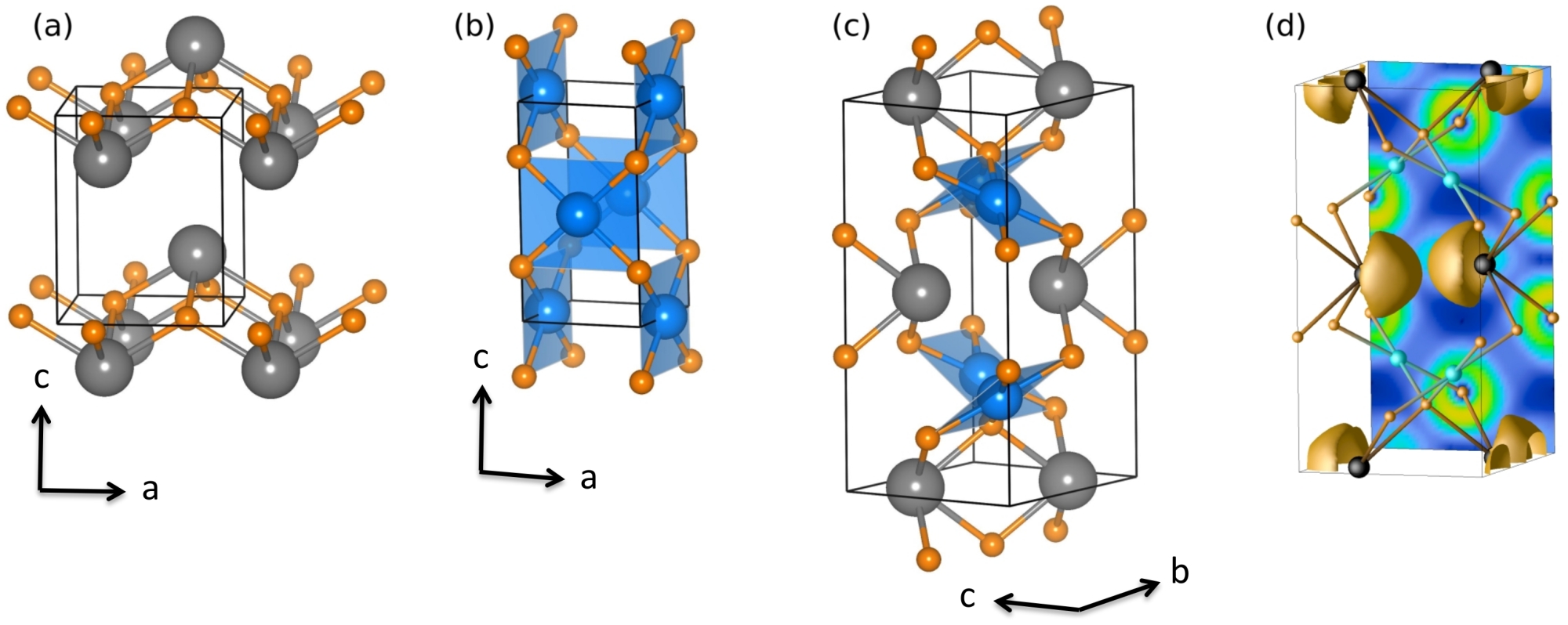
PbPdO2 is the only ternary oxide of Pb and Pd reported in the Inorganic Crystal Structures Database.[11] Single crystals of PbPdO2 were prepared by Meyer and Müller-Buschbaum, which they observed to be black.[12] Locally, the Pb-capped planes in -PbO and roughly square planar coordination of Pd in PdO are preserved in orthorhombic PbPdO2, which was determined to crystallize in the #74 space group. However, the relationship between the structural units is very distinct in this ternary phase [Figure 1(c)]. PbPdO2 can be viewed as a layered structure containing zig-zagging sheets of corner-sharing PdO4 planes, interleaved by layers of Pb. Oxygen is tetrahedrally coordinated to two Pd within the sheets and two Pd between the sheets. Between the Pd layers, edge-sharing PbO4 units form 1D chains running parallel to with Pb on alternating sides of the chain, and the chains are eclipsed with respect to one another along the axis.
While an understanding of the PbPdO2 structure is facilitated by describing it as a layered material, it is important to point out that chemically it should be regarded as a three-dimensional extended solid. The Pd–O and Pb–O bonds in the simple oxides of Pd and Pb are quite covalent, and PbPdO2 contains an extended network of –Pd–O–Pb–O–Pd– connectivities. There are two points that we emphasize here about the structure of PbPdO2: First, the dimensionality of the PdO4–PdO4 and PbO4–PbO4 connectivities are reduced in PbPdO2, relative to those in the oxides PdO and -PbO. Second, there are no edge-sharing PdO4 units present in PbPdO2 or any short Pd–Pd distances, as encountered in PdO, nor are there any in-plane Pd–O–Pd connectivities. Qualitatively, considering the structural arrangement and electronic configurations of the cations, one would expect PbPdO2 to not be any closer to metallic behavior than the two binary compounds that it is derived from.
Our interest in PbPdO2 stems from prior and ongoing efforts to understand relationships between the electronic structural features of platinum group and noble metal ions, and the catalytic activity of the oxides they form. We recently reported an experimental and computational comparison of the complex oxides of isoelectronic Pd2+ and Au3+, La2BaPdO5 and La4LiAuO8, both of which contain isolated PdO4 and AuO4 square planes, respectively.[13] Density functional calculations within the local density approximation (LDA) yielded sizeable (though underestimated) band gaps for both compounds, consistent with their yellow colors and optical absorption spectra. That LDA was a sufficient level at which to study these compounds is related to the isolated nature of the Pd and Au coordination environments. In contrast, although PdO is a well known semiconductor, LDA calculations often predict it to be metallic.[14]
The electronic structure of PdO has been previously studied by a variety of ab-initio methods. Hass et al. reported the first computational investigation of PdO, in which an augmented-spherical-wave approach within the local density approximation was employed.[15] PdO was correctly predicted to be a semiconductor, with a direct gap at the point, although the size of the gap was severely underestimated. A subsequent study reported by Park et al., using full-potential approaches with linearized augmented-plane-waves (LAPW) and linear-muffin-tin-orbitals (LMTO) within the LDA, was unable to predict a gap in PdO,[14] though a small gap was reported to open through the use of LMTO in the atomic-sphere-approximation.[16] Uddin et al. reported a study of density functional predictions for the electronic structure of PtO,[17] which is isostructural with PdO. Using Gaussian-type orbitals, the Heyd, Scuseria, and Ernzerhof screened hybrid functional[18] correctly predicted PtO to be a semiconductor, whereas calculations within the local spin-density approximation (LSDA), Perdew Burke and Ernzerhof (PBE) generalized gradient approximation (GGA), and with a meta-GGA functional, all led to the prediction of (poor) metallicity. Recently, a HSE band gap of 0.9 eV in PdO has been reported by Seriani et al.,[19] and Bruska et al. determined an HSE band gap of 0.8 eV that could be extended to 1.5 eV by increasing the amount of Fock exact exchange to 39 %.[20]
On the basis of LDA calculations, Wang suggested that PbPdO2 is a zero-gap oxide semiconductor,[21] with potentially very interesting electronic structural signatures when the compound is subject to partial substitution by magnetic ions. Chen et al. reported a combined experimental and computational study of PbPdO2, employing the PBE functional with the addition of a 2 eV Hubbard term on Pd to account for on-site Coulomb repulsion.[22] Their GGA+ calculations did not result in the opening of a band gap. However, Bennett et al. recently noted that an exceedingly large value of 8 eV, using the LDA+ method, was needed to reproduce the experimental gap of PdO.[23]
Electrical transport properties of polycrystalline PbPdO2 were reported by Ozawa et al.,[24] and Seebeck and Hall effect measurements indicated -type conductivity. It was suggested from a change in the temperature coefficient of resistance that PbPdO2 undergoes a metal-to-insulator transition at about 90 K, and that the ground state is an insulator, not a metal. However, the minimum resistivity of a little over 0.4 cm is more consistent with semiconducting behavior than it is with the resistivity of a metal, which is expected to be of the order of 10-2 cm or less. Additionally, the reported change in resistivity between the “insulating” and “metallic” states is less than a factor of 2, whereas typical metal-to-insulator transitions span two or more orders of magnitude. For comparison, Uriu et al. studied the effect of Li-substitution in PdO (Pd1-xLixO1-δ), and found that the resistivity at 273 K decreased from 3 cm in the unsubstituted material, to cm with 1 mol% Li, to cm with 8 mol% Li.[25]
Reports of chemical substitution in PbPdO2 – with the intent of introducing electrical carriers and/or magnetic ions – are few. Ozawa et al. studied the substitution of Cu for Pd, which increases the resistivity.[26] Magnetism and transport have been examined in Co and Mn substituted PbPdO2 by Lee et al.[27, 28] Both Co and Mn lower the resistivity, but the minima are pushed to higher and lower temperatures, respectively, relative to unsubstituted PbPdO2. The resistivity of PbPd0.9Co0.1O2 is larger than 0.1 cm at 150 K, while for PbPd0.9Mn0.1O2 the resistivity is 0.08 cm at 70 K.[28] Large electroresistance and magnetoresistance in PbPd0.75Co0.25O2 films have been reported by Wang et al.,[29] and quite recently, magnetism and transport properties of a PbPd0.81Co0.19O2 film were studied by Su et al.[30]
In the light of the electronic properties that would be expected for PbPdO2 on the basis of its structural attributes and electron count, we report density functional electronic structure calculations for PbPdO2 employing a screened hybrid functional (HSE06). Inclusion of exact exchange to the description of the short-range Coulomb potential has been shown to significantly enhance the accuracy of density functional calculations in periodic systems.[31, 32, 33, 34] To complement these results, we also present the HSE electronic structure of PdO. Additionally, by comparing the absolute positions, relative to the vacuum level, of the conduction band minima and the valence band maxima in -PbO, PdO and PbPdO2, we find that facile electron transfer from PbPdO2 to, for example, residual PdO left from the preparation, may account for the -type conductivity observed in nominally pure materials. The HSE calculations suggest surprisingly linear dispersions of the valence and conduction bands across the direct 1.1 eV band gap of this compound.
2 Computational methods
Density functional electronic structure calculations were performed in the Vienna ab initio Simulation Package (VASP).[35, 36] Interaction between the valence and core electrons was described using the projector augmented wave (PAW) approach,[37, 38] with valence electrons described by plane-wave basis sets. 14 valence electrons were included for Pb (5d106s26p2), 10 valence electrons for Pd (4d10), and 6 valence electrons for O (2s2p4). Calculations were performed at the scalar relativistic level, without the inclusion of spin-orbit coupling, using both the GGA of Perdew, Burke, and Ernzerhof (PBE),[39] and the hybrid functional described by Heyd, Scuseria, and Ernzerhof (HSE06).[18, 40] The screened hybrid functional introduces a percentage of exact nonlocal Fock exchange (25 %) to the PBE functional, and a screening of 0.2 Å-1 is applied to partition the Coulomb potential into long-range and short-range terms. Hartree-Fock and PBE exchange mix in the short-range portion, with the long-range exchange represented by the PBE functional.
A cutoff energy of 520 eV was used in all calculations, as were -centered -point grids. Relaxations were deemed to have converged when the forces on all the atoms were less than 0.01 eV Å-1. Geometry optimization of PbPdO2 was performed in the primitive rhombohedral unit cell, using a -mesh. The same grid was also used to calculate the HSE electronic density of states (DOS). PBE calculations of the PbPdO2 DOS employed a -mesh. Band structure calculations for PbPdO2 were performed using the conventional orthorhombic unit cell. For PdO, a -mesh was used to relax the structure with the HSE functional and to calculate the DOS. PBE relaxation and DOS calculations for PdO employed and -point meshes, respectively. PBE band structures were calculated with 30-point interpolations between each high symmetry point. HSE band structure calculations are presented only along the dispersions in the region of the band gaps, to to for PbPdO2, and to to for PdO, using 10-point interpolations between each high symmetry -point.
To investigate the doping tendencies of PbPdO2, the positions of the valence band maximum (VBM) and the conduction band minimum (CBM), relative to vacuum, were studied. Slab models were constructed and atomic positions optimized using the PBE functional with fixed lattice parameters. Four Pb–O–Pd–O bilayers were included in PbPdO2 slab, eight Pd–O layers were used in the PdO slab, and eight PbO layers were used for the PbO slab. The lengths of the ideal slabs for the three compounds are 19.20 Å, 21.82 Å and 17.80 Å, respectively. Vacuum regions with the same length as the slab were included for each compound. Because the local and semi-local PBE functional usually generates band gaps significantly smaller than the experimental values, the hybrid HSE functional was employed for static calculations of the PBE relaxed slabs. To obtain the positions of the VBM and CBM relative to the vacuum level, the electrostatic potential in the center of the slabs (assuming it well represents the bulk) were aligned with the center of the vacuum region.
Linear Muffin-Tin Orbital (LMTO) calculation,[41, 42] performed within the atomic sphere approximation using version 47C of the Stuttgart TB-LMTO-ASA program,[43] was used in the determination of the electron localization function (ELF) for PbPdO2. Scalar-relativistic Kohn–Sham equations within the local density approximation [44] were solved taking all relativistic effects into account except for the spin-orbit coupling. The calculation was performed on 527 irreducible -points within the conventional orthorhombic cell. The ELF provides a measure of the local influence of the Pauli repulsion on the behavior of electrons, enabling the real-space mapping of core, bonding, and non-bonding regions in a crystal.[45, 46]
3 Results and disucssion
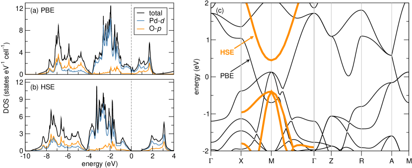
The total electronic and Pd-d and O-p orbital projected density of states for PdO, calculated using the PBE and HSE functionals, are compared in panels (a) and (b) of Figure 2. The PBE band-structure is shown in panel (c) in the region of the valence band maximum (VBM) and conduction band minimum (CBM), with bands from the HSE calculation overlaid in bold lines along the dispersion from to to . Structural parameters obtained for the PBE and HSE relaxed structures are listed in Table 1, along with experimentally determined values for comparison. Oxygen p-states lie predominantly between 9 eV and 4 eV, with Pd d-states more densely populated between 4 eV and the Fermi energy, referenced to the top of the valence band in the DOS plots and denoted with dashed vertical lines. In the plot of the band structure, 0 eV represents the Fermi energy for the PBE calculation. The Fermi energy of bands calculated with HSE have been adjusted to the absolute energy of the PBE . Stabilization of the VBM and destabilization of the CBM by HSE occur in almost equal amounts. Note the wide energy dispersion of bands at the top of the valence band and bottom of conduction band, derived from Pd dxy and d orbitals, respectively.
The use of PBE leads to the prediction of poorly metallic character in PdO. HSE, on the other hand, correctly predicts PdO to be a semiconductor. What we emphasize here is not the magnitude of the gap predicted by HSE, which is a little less than 1 eV, but rather that HSE affords a qualitative prediction that agrees well with the known electronic structure of PdO. The size of the gap is of the right order, but given the disparities in the experimental gaps reported for PdO we cannot comment on whether the prediction is an over- or under-estimate.
-
PBE HSE expt. PBE HSE expt. PdO PbPdO2 (Å) 3.10 3.07 3.043 9.61 9.46 9.455 (Å) 5.53 5.45 5.460 (Å) 5.44 5.33 5.336 4.77 4.77 4.660 Pb 0.772 0.764 0.774 O 0.350 0.350 0.345 Pd–O (Å) 2.06 2.03 2.02 2.06 2.04 2.01 Pb–O (Å) 2.38 2.34 2.37 O–Pd–O (∘) 97.5 98.1 97.5 95.8 96.2 94.3
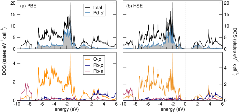
Geometry-optimized structural parameters obtained with the PBE and HSE functionals are given in Table 1, and the total electronic and orbital projected DOS of PbPdO2 are presented in Figure 3. The shape and dispersion of the orbital contributions obtained by the different methods are quite similar, with the obvious difference being the presence of a 1.1 eV bandgap in the HSE electronic structure. The upper panels display the total and Pd-d projected DOS, which are shaded for clarity, and the lower panels show the O-p, Pb-p and Pb-s projected DOS. The bottom of the Pd-d band in PbPdO2 is somewhat destabilized (closer in energy to ), relative to the dispersion of the d states in PdO, and this is consistent with decreased overlap associated with the absence of short Pd–Pd distances. Note the strong hybridization of O-p and Pb-s states between 10 eV and 8 eV, and overlap of O-p and Pb-s and p states states near the Fermi energy, features that are similarly encountered in the electronic structure of -PbO.[47, 48] In -PbO, the highly stabilized Pb-s and O-p states held deep below the are strongly bonding, while the states just below are of antibonding character.[49] The mixing of Pb-s and O-p states near the Fermi energy has been suggested to drive the localization of the Pb lone pair into lobe-shaped structures.[47, 48] As can be seen in the electron localization function (ELF) isosurface of PbPdO2 shown in panel (d) of Figure 1, the Pb lone pair lobes are localized apical to the base of the Pb-capped planes.
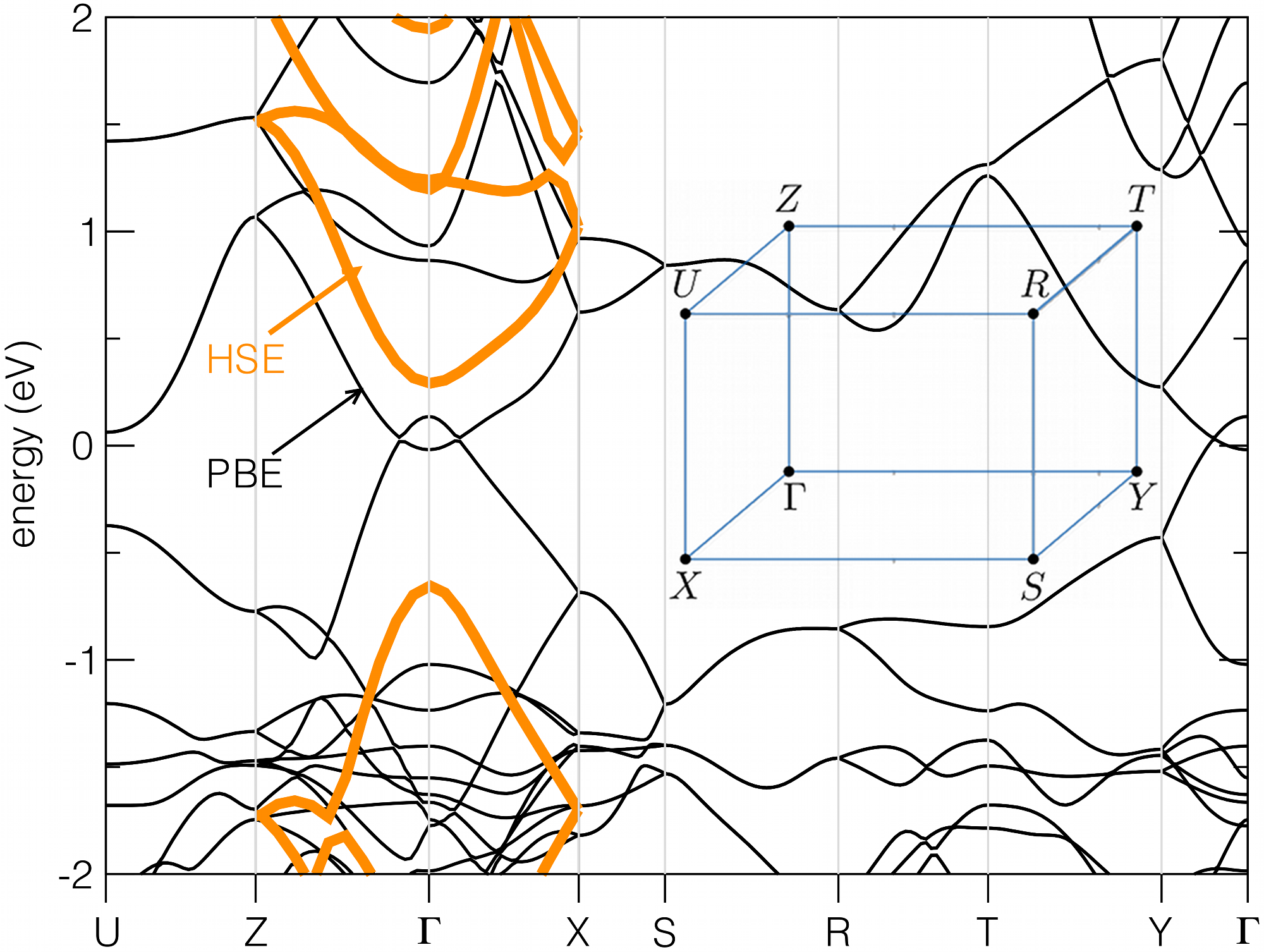
The PBE band structure of PbPdO2 in the vicinity of the Fermi energy is shown in Figure 4, with the HSE calculated bands overlaid in bold along the to to dispersion. For the PBE calculation 0 eV is taken as the Fermi energy, while for the HSE calculation the Fermi energy has been adjusted to the absolute energy of the PBE . Band structure calculations were performed using the Brillioun zone (BZ) for a conventional orthorhombic cell, and the BZ is inset in Figure 4 for convenience. The PBE calculated band structure shows a slight crossing of bands at the point, where a zero-gap was predicted by Wang.[21] A direct gap is clearly evident in the dispersion calculated with HSE. It is important to note that the bands at the top of the valence band and at the bottom of the conduction band do not show nearly as much energy dispersion as the equivalent bands in PdO. Also noted is the surprising linearity of the valence and conduction band dispersions near the direct band gap.
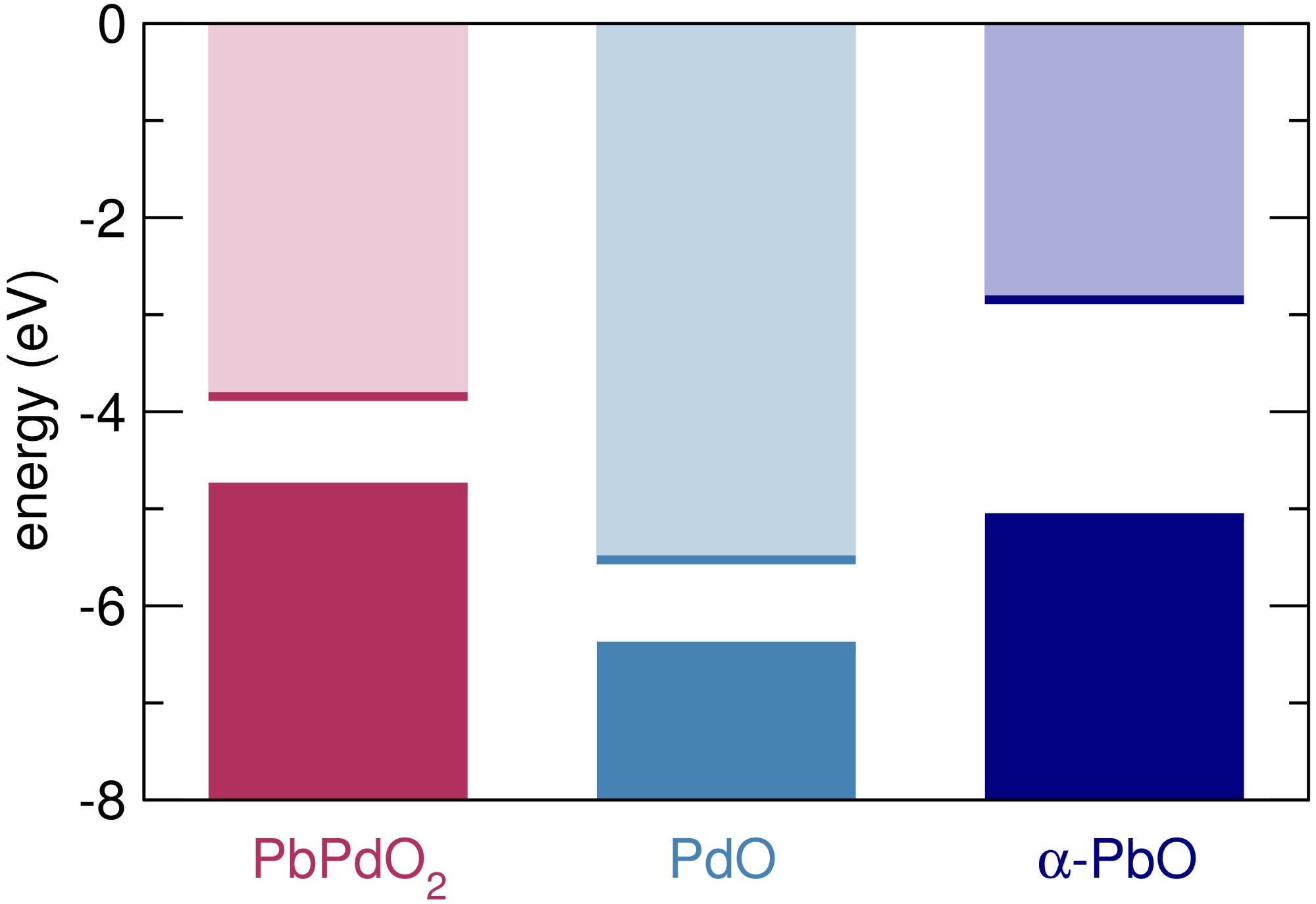
In Figure 5 we present a schematic showing the calculated positions of the valence band maxima (VBM) and conduction band minima (CBM) for PbPdO2, PdO, and -PbO. The VBM and CBM positions of PbPdO2 are 4.78 eV and 3.84 eV below vacuum, respectively, which are quite high. This indicates that the compound is prone to -type doping by native defects and intentional substituents. Conversely, the VBM and CBM of PdO are 6.42 eV and 5.53 eV below the vacuum, indicating that PdO is, in comparison with PbPdO2, more prone to being -doped. More importantly, the CBM of PdO is lower in energy than the VBM of PbPdO2. Thus, the presence of PdO in a sample of PbPdO2 can lead to hole-doping of PbPdO2 by facile electron transfer from its valence band to the conduction band of PdO. Even small amounts of PdO would lead to the generation of a large quantity of holes in the valence band of PbPdO2, which may explain the -type conductivity observed for samples of PbPdO2.
On the other hand, the VBM and CBM for -PbO are located at 5.09 eV and 2.85 eV below vacuum, respectively. Because PbO is more ionic, it has a larger gap, and its VBM is lower than the VBM of PbPdO2 while the CBM of PbO is higher than the CBM of PbPdO2. Therefore, the presence of unreacted PbO in samples of PbPdO2 are not likely to significantly affect its electronic properties, such as the density of charge carriers. Given the volatility of PbO, PdO is much more likely to persist in samples of PbPdO2.
Our calculations only address alignment of the energy levels of the starting materials typically used in the preparation of PbPdO2, relative to the target phase. A complete discussion of the source of hole conductivity requires a comprehensive study of the defect and impurity properties of the system – as they may contribute greatly to the source of the -type doping – which is beyond the scope of the present work. However, our results reveal that PbPdO2 is susceptible to -type doping, and emphasizes the importance of preparing high purity materials as small amounts of residual starting material, PdO in particular, may greatly influence the physical properties observed in this system.
4 Conclusions
In conclusion, electronic structure calculations carried out on PbPdO2 at the hybrid HSE level suggest that the ground state of PbPdO2 is actually that of a small band gap semiconductor. Slab calculations to obtain the locations of the valence and conduction bands with respect to the vacuum level suggest that PbPdO2 can be easily hole-doped. Both these observations are consistent with experimental observations on the system. The valence band dispersion in this easily hole-doped material is surprisingly linear, potentially suggesting interesting low-temperature physics in this compound.
Acknowledgments
We thank the Department of Energy, Office of Basic Energy Sciences for support of this work through Grant No. DE-FG02-10ER16081. This work made use of the computing facilities of the Center for Scientific Computing supported by the California Nanosystems Institute, Hewlett Packard, and by the Materials Research Laboratory at UCSB: an NSF MRSEC (DMR-1121053). JAK thanks Kris Delaney and David Scanlon for helpful discussions pertaining to the use of hybrid density functionals.
References
References
- [1] R. Seshadri. Proc. Indian Acad. Sci., 113:487–496, 2001.
- [2] M. S. Hegde, Giridhar Madras, and K. C. Patil. Acc. Chem. Res., 42:704–712, 2009.
- [3] R. C. Keezer, D. L. Bowman, and J. H. Becker. J. Appl. Phys., 39:2062–2066, 1968.
- [4] W. J. Moore and L. Pauling. J. Am. Chem. Soc., 63:1392–1394, 1941.
- [5] D. B. Rogers, R. D. Shannon, and J. L. Gillson. J. Solid State Chem., 3:314–316, 1971.
- [6] F. Hulliger. J. Phys. Chem. Solids, 26:639–645, 1965.
- [7] H. Okamoto and T. Aso. Jap. J. Appl. Phys., 6:779, 1967.
- [8] T Pillo, R Zimmermann, P Steiner, and S Hufner. J. Phys. Condens. Matter, 9:3987–3999, 1997.
- [9] P. O. Nilsson and M. S. Shivaraman. J. Phys. C. Solid State Phys., 12:1423–1427, 1979.
- [10] E. Rey, M. R. Kamal, R. B. Miles, and B. S. H. Royce. J. Mater. Sci., 13:812–816, 1978.
- [11] A. Belsky, M. Hellenbrandt, V. L. Karen, and P. Luksch. Acta Cryst. B, 58:364–369, 2002.
- [12] H. Meyer and H. Müller-Buschbaum. Z. Anorg. Allg. Chem., 442:26–30, 1978.
- [13] J. A. Kurzman, X. Ouyang, W. B. Im, J. Li, J. Hu, S. L. Scott, and R. Seshadri. Inorg. Chem., 49:4670–4680, 2010.
- [14] K. T. Park, D. L. Novikov, V. A. Gubanov, and A. J. Freeman. Phys. Rev. B, 49:4425–4431, 1994.
- [15] K. C. Hass and A. E. Carlsson. Phys. Rev. B, 46:4246–4249, 1992.
- [16] R. Ahuja, S. Auluck, B. Johansson, and M. A. Khan. Phys. Rev. B, 50:2128–2132, 1994.
- [17] J. Uddin, J. E. Peralta, and G. E. Scuseria. Phys. Rev. B, 71:155112, 2005.
- [18] J. Heyd, G. E. Scuseria, and M. Ernzerhof. J. Chem. Phys., 118:8207, 2003.
- [19] N. Seriani, J. Harl, F. Mittendorfer, and G. Kresse. J. Chem. Phys., 131:054701, 2009.
- [20] M. K. Bruska, I. Czekaj, B. Delley, J. Mantzaras, and A. Wokaun. Phys. Chem. Chem. Phys., 13:15947–15954, 2011.
- [21] X. L. Wang. Phys. Rev. Lett., 100:156404, 2008.
- [22] S. W. Chen, S. C. Huang, G. Y. Guo, J. M. Lee, S. Chiang, W. C. Chen, Y. C. Liang, K. T. Lu, and J. M. Chen. Appl. Phys. Lett., 99:012103, 2011.
- [23] J. W. Bennett, I. Grinberg, P. K. Davies, and A. M. Rappe. Phys. Rev. B, 82:184106, 2010.
- [24] T. C. Ozawa, T. Taniguchi, Y. Nagata, Y. Noro, T. Naka, and A. Matsushita. J. Alloys Compd., 388:1–5, 2005.
- [25] R. Uriu, D. Shimada, and N. Tsuda. J. Phys. Soc. Jpn., 60:2479–2480, 1991.
- [26] T. C. Ozawa, T. Taniguchi, Y. Nagata, Y. Noro, T. Naka, and A. Matsushita. J. Alloys Compd., 395:32–35, 2005.
- [27] K. J. Lee, S. M. Choo, J. B. Yoon, K. M. Song, Y. Saiga, C. Y. You, N. Hur, S. I. Lee, T. Takabatake, and M. H. Jung. J. Appl. Phys., 107:09C306, 2010.
- [28] K. J. Lee, S. M. Choo, Y. Saiga, T. Takabatake, and M.-H. Jung. J. Appl. Phys., 109:07C316, 2011.
- [29] X. Wang, G. Peleckis, C. Zhang, H. Kimura, and S. Dou. Adv. Mater., 21:2196–2199, 2009.
- [30] H. L. Su, Huang. S. Y., Y. F. Chiang, J. C. A. Huang, C. C. Kuo, Y. W. Du, Y. C. Wu, and R. Z. Zuo. Appl. Phys. Lett., 99:102508, 2011.
- [31] J. Heyd and G. E. Scuseria. J. Chem. Phys., 121:1187–1192, 2004.
- [32] J. Heyd, J. E. Peralta, G. E. Scuseria, and R. L. Martin. J. Chem. Phys., 123:174101, 2005.
- [33] B. G. Janesko, T. M. Henderson, and G. E. Scuseria. Phys. Chem. Chem. Phys., 11:443–454, 2009.
- [34] T. M. Henderson, J. Paier, and G. E. Scuseria. Phys. Status Solidi B, 248:767–774, 2011.
- [35] G. Kresse and J. Hafner. Phys. Rev. B, 49:14251, 1994.
- [36] G. Kresse and J. Furthmüller. Phys. Rev. B, 54:11169, 1996.
- [37] P. E. Blöchl. Phys. Rev. B, 50:17953, 1994.
- [38] G Kresse and D Joubert. Phys. Rev. B, 59:1758–1775, 1999.
- [39] J. P. Perdew, K. Burke, and M. Ernzerhof. Phys. Rev. Lett., 77:3865, 1996.
- [40] A. V. Krakau, O. A. Vydrov, A. F. Izmaylov, and G. E. Scuseria. J. Chem. Phys., 125:224106, 2006.
- [41] O. K. Andersen. Phys. Rev. B, 12:3060, 1975.
- [42] O. Jepsen and O. K. Andersen. Z. Phys. B, 97:35, 1995.
- [43] O. Jepsen and O. K. Andersen. The Stuttgart TB-LMTO-ASA Program version 47, MPI für Festkörperforschung, Stuttgart, Germany. 2000.
- [44] U. von Barth and L. Hedin. J. Phys. C, 5:1629, 1972.
- [45] A. D Becke and K. E. Edgecombe. J. Chem. Phys., 92:5397, 1990.
- [46] B. Silvi and A. Savin. Nature, 371:683, 1994.
- [47] G. W. Watson, S. C. Parker, and G. Kresse. Phys. Rev. B, 59:8481–8486, 1999.
- [48] G. W. Watson and S. C. Parker. J. Phys. Chem. B, 103:1258–1262, 1999.
- [49] J.-M. Raulot, G. Baldinozzi, R. Seshadri, and P. Cortona. Solid State Sci., 4:467–474, 2002.