Comparison of microscopic models for disorder in bilayer graphene: Implications for the density of states and the optical conductivity
Abstract
We study the effects of disorder on bilayer graphene using four different microscopic models and directly compare their results. We compute the self-energy, density of states, and optical conductivity in the presence of short-ranged scatterers and screened Coulomb impurities, using both the Born approximation and self-consistent Born approximation for the self-energy. We also include a finite interlayer potential asymmetry which generates a gap between the valence and conduction bands. We find that the qualitative behavior of the two scattering potentials are similar, but that the choice of approximation for the self-energy leads to important differences near the band edge in the gapped case. Finally, we describe how these differences manifest in the measurement of the band gap in optical and transport experimental techniques.
I Introduction
The current interest in bilayer graphenedassarma-rmp2011 ; abergel-advphys2010 is motivated largely by the possibility of its application in the designing of novel electronic devices, as well as the opportunity to investigate the fundamental physics of massive chiral electrons in a condensed matter setting. In particular, the opportunity to open a dynamically tunable band gap by electronic gating was predicted theoretically mccann-prb2006 , and verified in optical experiments ohta-sci2006 ; zhang-nature2009 ; mak-prl2009 ; kuzmenko-prb2009 ; li-prl2009 , and this presents an opportunity not currently available in traditional two-dimensional electron systemsando-rmp1982 . However, transport measurements oostinga-natmat2007 ; zou-prb2010 ; xiao-prb2010 ; yan-nl2010 ; xia-nl2010 ; taychatanapat-prl2010 ; jing-nl2010 demonstrate that the full nature of the effects of disorder induced in the graphene by its environmentmucciolo-jpcm22 is not currently resolved. This is a crucial issue since it appears that environmental disorder is the main limitation on the favorable properties of bilayer graphene devices. In particular, there is a wide discrepancy in the size of the band gap extracted from transport measurements (which has obvious negative impact on the application of bilayer graphene in switching devices) and significant variation in the sub-gap conductivity as a function of temperature. At low temperature, variable range hopping via midgap states dominates and produces a relatively small value for the gap, while at higher temperature, thermally activated transport between the band tails is the predominant mechanismyan-nl2010 . It has been suggested dassarma-prb2010 ; hwang-prb2010 that both charged impurity disorder and short-range defect scattering play a role in transport properties of bilayer graphene and the puddling of electrons due to charged impurity disorder was also shown to be crucial in the understanding of capacitance measurements of dual-gated bilayer grapheneabergel-prb2011 ; young-arXiv ; henriksen-prb2010 . A very recent work rossi-arXiv shows that the percolation transport gap and the spectral band gap could be significantly different in bilayer graphene due to the strong potential fluctuation and density inhomogeneity induced by electron-hole puddles arising from random charged impurities in the environment. Therefore, disorder is a key effect in many different measurements and a thorough understanding of the microscopic origin and effects of impurities and other scatterers is highly important.
Previously, theoretical study of the role of disorder in bilayer graphene has been undertaken koshino-prb2006 ; bena-prl2008 ; nilsson-prb2008 ; ando-jpsj2011 ; ferreira-prb2011 ; yuan-prb2010 ; castro-prl2010 ; mkhitaryan-prb2008 ; dahal-prb2008 ; nilsson-prl2007 in which several types of disorder (such as resonant scatterers, lattice vacancies, short-range scatterers, and generic scattering processes) were investigated within a variety of theoretical schemes (such as the coherent potential approximation, the Born approximation and self-consistent Born approximation, as well as other numerical techniques). The effect of disorder on the density of states (DOS), dc and ac conductivities, and other physical quantities were studied. However, to date, there has not been a systematic comparison of the most physical scattering mechanisms – charged impurity disorder and short-range scatterers – for different approximation schemes. This is the topic of the current article. In this paper, we present a comprehensive analysis of the effect of charged impurity disorder and short-range scatterers on the DOS and optical conductivity of bilayer graphene in the presence of a band gap created by electrostatic gating. We compare these two scattering mechanisms which model the electron-impurity interaction, and two approximations to the self-energy induced by this interaction in the perturbation theory. Specifically, we consider the screened electron–impurity Coulomb interaction (CI) and the short-ranged interaction (SRI) modeled as a -function potential in real space as the model disorder potentials for our study. This paper is the first analysis which treats these two scattering mechanisms on an equal footing and makes direct comparisons between them, since previous works have treated only different forms of short-ranged electron–impurity interactions, and we extend our analysis of the CI presented previouslymin-prb2011 . For both of the these electron–impurity interaction potentials, we describe the Born approximation (BA) and self-consistent Born approximation (SCBA) and highlight the differences between these two levels of approximation in the perturbation theory. We also consider both the gapped and gapless situations. It should be noted that some of the numerical techniques which were previously applied to the electron–impurity interaction ferreira-prb2011 ; yuan-prb2010 technically go beyond the BA and SCBA and their application to the gapped case would be desirable. However, we believe that particularly the SCBA will capture the relevant physics near the band edge.
Although our main interest is a comprehensive theoretical formal understanding of disorder effects on bilayer electronic properties using a number of different models, a strong motivation for our work is the large discrepancy between the experimentally extracted transport gap in bilayer graphene and the theoretically calculated band gap obtained from band structure calculations. We also want to understand the effect of disorder on the optical conductivity of bilayer graphene since extracting an optical band gap from the optical conductivity data is non-trivial in the presence of strong disorder (although it is routinely done in the literature, often incorrectly in our view). Our work should have implications for the bilayer density of states (and hence the transport gap) and the optical gap extracted from optical measurements. We also mention a particular advantageous feature of our theory is that we use the accurate four band model for bilayer graphene throughout this work and retain the contributions from all four bands, avoiding various simplifications used in the theoretical literature dealing with bilayer graphene.
The structure of this paper is as follows. In Sec. II we describe the self-energy of electrons in bilayer graphene using the short-range and Coulomb scattering potentials for the BA and SCBA, and in Sec. III we apply the resulting Green’s functions to compute the DOS. In Sec. IV we describe the optical conductivity and then in Sec. V we focus on the highly important issue of the band gap and how it is extracted from various experimental techniques and describe the role of disorder in that context. Finally, we summarize our results in Sec. VI and highlight the most important conclusions of our work. Two appendices contain additional results: A scheme to use the computationally efficient SRI to approximate the CI for low carrier density, and the derivation of the optical conductivity.


We now introduce the single-particle theory which underlies our considerations of disorder. Throughout this paper, we use the four band tight-binding model for bilayer graphene but neglect next-nearest neighbor hoppings between the two layers. We label the electron states with the band index for the conduction and valence bands, and with the branch index for the low-energy and split bands. The dispersion of the four bands is given by the equationabergel-advphys2010 ; mccann-prb2006
| (1) |
where labels the band, for the conduction (valence) band, and for the split (low-energy) branch [see Fig. 1(a)], and . The inter-layer coupling in the tight binding formalism is , and is the Fermi velocity of monolayer grapheneabergel-advphys2010 ; dassarma-rmp2011 . This band structure is isotropic in the wave vector and symmetric between conduction and valence bands. In the presence of an external electric field perpendicular to the plane of the graphene, an asymmetry is introduced in the potential on the upper and lower layers which generates a gap between the and bands at low energy. This gap is parameterized by the energy , corresponding to the energy difference between the two bands at . However, the minimum of the band gap is found at a wave vector and is given by . This is known as the “sombrero” shape. We do not include various next-nearest neighbor interlayer hops which have been considered elsewheredassarma-rmp2011 ; abergel-advphys2010 . We justify this by noting that, for example, the energy of the inter-band optical transitions near the K point are only modified by a few percent of the interlayer coupling when these hops are included. In a similar way, while there will be some small quantitative difference in the DOS due to inclusion of these higher order terms, the position of the band edge is almost unchanged and the disorder is by far the dominant effect. Therefore the simple tight-binding model we outline is sufficient to obtain an accurate description of the DOS and optical conductivity in the presence of disorder.
The two-dimensional CI in momentum space is
| (2) |
where is the distance of the impurities from the graphene surface, is the effective dielectric constant of the system, and is the screening wave vector, which can in principle be a function of . In the extrinsic case (i.e. when there is a finite density of electrons or holes in the graphene so that ), the screening is taken into account in the Thomas-Fermi approximationhwang-prb2007 so that the dependence of the screening wave vector is constant and
| (3) |
where is the non-disordered D OS at the Fermi energy. This screening wave vector is shown in Fig. 1(d) as a function of the Fermi energy. In the ungapped case (dashed line), the DOS is finite for all values of so is well defined. The shape of the DOS is replicated in so that it increases linearly except for the onset of the split bands which causes a step in the DOS at . Note that this linear increase is a result of the more accurate hyperbolic model which we use for the dispersion of bilayer graphene near the K point. The quadratic approximation is only valid at low density and predicts a constant DOS, however the density ranges we consider exceed the applicability of this modelhwang-prl2008 . When the gap is present, the DOS is a more complex function which is reflected in [solid line in Fig. 1(d)]. In particular, it is divergent at the band edge so that the screening becomes very strong for low carrier density. For intrinsic bilayer graphene (that is, when the carrier density is zero so that ) in the gapped regime, the density of states is not defined and some other approximation to the screening wave vector must be made to avoid the unphysical divergence of the Coulomb interaction at . In Fig. 1(e), we show the screening wave vector as a function of in the random phase approximation (RPA) for intrinsic bilayer graphene. This shows that for the value is finite, which is consistent with an earlier analysis of the screening in bilayer graphenehwang-prl2008 computed using a quadratic approximation for the band structure. For , the low- behavior is almost linear with the value being zero. In both cases, the screening wave vector depends linearly on at high wave vector. Therefore, the limit shows that this more sophisticated approximation also fails to remove the divergence in for gapped bilayer graphene. In order to make an order-of-magnitude estimate for the screening in this case, we take the extrapolation of the higher-energy screening wave vector to [as shown by the dotted line in Fig. 1(d)]. For , this means where is the lattice constant. The precise value chosen will not significantly affect the DOS or optical conductivity. The regularization of the CI at is necessary for avoiding and artificial divergence, but the details of this infrared regularization do not affect the results presented in this paper.
The short-range interaction (SRI) is given by the potential
| (4) |
where the interaction strength is parameterized by . In principle, the parameter is not known so it can either be used as a fitting parameter, or some physical reasoning can be used to estimate its value. We make a phenomenological assumption that where is the scattering cross-section of the short-ranged impurities. We assume that and that the sample is mounted on an SiO2 substrate so that is the effective dielectric constant of the environment, giving . In Appendix A we demonstrate a way in which the SRI can be used to approximate the CI in the low-energy region. Our models of long- and zero-ranged disorder give similar results at low energies (see Appendix A) so our model also applies in this energy range to the intermediate-range resonant scattering disorder. In the literature, it is noted that the resonant scatterers are likely to also contribute to the existence of mid-gap states in the system which, as far as we know, have never been observed in any optical experiments. We do not take these mid-gap states into account in our model, but mention that it should be straightforward to include such states in our theory if experiments demonstrate their existence.
II Self-energy

In this section, we describe the self-energy introduced by interaction between the electrons and the impurities in bilayer graphene. We use two approximations, the BA and the SCBA, and compare the results of each. Formally, the self-energy in the BA is
| (5) |
and in the SCBA is
| (6) |
which differs from the BA because it includes the full Green’s function on the right-hand side and therefore defines a self-consistent equation for the self-energy. The SCBA self-energy is generally found by iterating this expression taking the BA as the initial value of the self-energy on the right-hand side until convergence is reached. The diagrams corresponding to these approximations are shown in Fig. 1(b,c). Although the SCBA is a self-consistent approximation involving an infinite series of diagrams, it is not always necessarily better that the BA since in each order many diagrams (e.g. the crossing diagrams) are left out – in general, the self-consistency in the SCBA tends to smooth out the sharp features in the BA results as we shall see below in our calculations of the DOS. In these equations, the symbol is the areal density of charged impurities, is the electron-impurity interaction potential for the wave vector , is the wave function overlap between and states, and is a positive infinitesimal. In the following we shall describe the self-energy of both the CI and the SRI each of which requires the appropriate expression for the interaction potential [Eq. (2) or Eq. (4)] to be substituted into the equations for the self-energy. Because the bands are electron-hole symmetric, we also have the symmetry relation
| (7) |
The real and imaginary parts of these self-energies are plotted in Fig 2. Specifically, we take wave vector , impurity concentrations and , corresponding to a back-gated SiO2 sample, and two values of the gap: and as indicated by the labels in Fig. 2. The solid lines refer to the band, the dashed lines to the band. The and bands can be found via Eq. (7). In the CI case, we have taken to define the screening wave vector. Throughout this article, we have , which gives , and . In the SRI/BA, the factor is a multiplier, meaning that the lines for the different impurity concentrations are scaled copies of each other, but this is not the case for the CI or for the SCBA. We see that the BA and SCBA give rather similar results for most values of energy, especially in the gapless case. However, the sharp spikes in the BA due to band edges are rounded off in the SCBA, and the onset of the imaginary part at the band edge is shifted to slightly lower energy in the SCBA. These differences will be manifest in the DOS at the band edge as we discuss below. In the case, the imaginary part of the low-energy branch is always finite, and is roughly constant up to the energy where the split bands become occupied. When is finite, the imaginary part disappears in the region near signifying that a gap has opened. Large peaks appear near the band edge, and these peaks are not symmetrical in energy, but are larger on the positive energy (conduction band) side of the gap. This behavior is reversed in the valence band due to the relation in Eq. (7). The presence of the gap also modifies the inter-band contribution to the self-energy, reducing the size of the imaginary part in the higher energy regions. In addition to the change in the relative size of the self-energy, increasing impurity concentration has the effect of introducing a larger shift to the energy at which the band minima occur.
III Density of states

These self-energies described in Section II define Green’s functions which can be used to compute the DOS as
| (8) |
where and are the spin and valley degeneracies respectively, and is the Green’s function incorporating the self-energy induced by the electron-impurity interaction (see Fig. 1). The DOS for the clean system is found by substituting (where is a positive infinitesimal) or by exact extraction from the band structure. The DOS functions are shown in Fig. 3 for the BA and the SCBA, for the CI and SRI, at two different values of impurity concentration, and for the ungapped and gapped cases. In the gapless situation (top row of Fig. 3) the only difference between the two approximations is a slight rounding-off of the step at the onset of the split bands in the SCBA. For our choice of parameters, the SRI gives a stronger change in the slope of the DOS with increasing impurity density than the CI, leading to a larger change in the DOS at higher energies. Also, increasing impurity concentration shifts the bottom of the split bands to lower energy, as indicated by the position of the step-like feature. In the gapped case (middle row of Fig. 3), increasing impurity concentration has the marked effect of lowering the energy of the onset of the low-energy band. In fact, if the disorder is sufficiently strong (and the clean band gap is not too large), the gap can be closed by disorder broadeningmin-prb2011 . Also, when the gap is present the features of the band edge are qualitatively different between the BA and the SCBA. Specifically, the divergence present in the clean DOS at the band edge persists as a sharp spike in the BA, but is rounded off in the SCBA, indicating that the DOS approaches zero in the low-density limit for the SCBA but continues to diverge in the BA. Probes which are sensitive to the DOS, such as the tunneling conductance in atomic force microscopy, capacitance measurements, or direct measurement of via single electron transistor spectroscopy should be sensitive to this difference at low carrier density. To highlight this difference, in the bottom row of Fig. 3 we show the low-energy conduction band edge for three different values of the impurity density for each pair of self-energy and scattering potential approximations. In the BA [Fig. 3(c,i)], increasing disorder decreases the height of the peak at the band edge, and creates a dip in the region where the band edge would be in the non-disordered case which widens with increasing impurity density. The SCBA shows very different behavior at the band edge. The sharp peak disappears, and the onset of the finite density of states occurs at a slightly lower energy than in the BA. The CI and the SRI give similar results for the modification of the band edge (except that the SRI is stronger for equivalent choice of because of our choice of ) indicating that the SRI can even be used to reliably approximate the low-density behavior of the DOS in the CI case as long as is set correctly, as described in Appendix A. The reason for this is that the screening wave vector is of the order of the size of the Brillouin zone [see Fig 1(d)] which is large in comparison with the wave vectors near the K point which dominate the contribution to the Green’s function at low energy. Therefore, the dependence in is negligable at this energy scale and the interaction strength is almost independent of , just as it is in the short-range case. However, for all impurity densities and for both approximations, the DOS remains close to the non-disordered value away from the band edge with the disorder broadening affecting the DOS mainly near the band edge.
IV Optical conductivity

We now turn our attention to the optical conductivity of gapped bilayer graphene. This is an important quantity from the experimental perspective since the optical identification of graphene blake-apl2007 ; abergel-apl2007 and the optical determination of the band gapli-prl2009 ; kuzmenko-prb2009 ; mak-prl2009 both depend crucially on a thorough understanding of the optical conductivity. The optical conductivity in the absence of disorder was calculated some time ago nicol-prb2008 ; min-prl2009 , but we extend this analysis to include the effects of disorder using the same CI and SRI models discussed before. The optical conductivity is given by
| (9) |
where
| (10) |
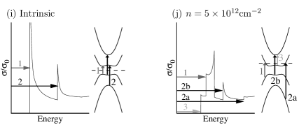
The derivation of these equations is given in Appendix B. We use and show the results in Fig. 4 for the four combinations of scattering mechanism and approximation for the self-energy. Figure 4(a)–(d) show the intrinsic case, and the origin of each of the features in the curves is sketched in Fig. 4(i). In the CI shown in Fig. 4(a–b), the peak associated with the interband transitions is shifted to lower energy with increasing disorder. In the BA [Fig. 4(a)] the sharp spike at the band edge persists even in the presence of strong disorder, while in the SCBA, [Fig. 4(b)] it is rounded off and a significant tail develops. Also, in the BA, there is a small peak near the energy which is an artifact of this approximation and is not present in the SCBA. These features directly reflect the related structure in the DOS. Comparing with the short-range interaction in Fig. 4(c–d), it is clear that the qualitative behavior of the optical conductivity near the band edge is identical to the CI. However, because the strength of the interaction remains constant at large wave vectors, the structure near the onset of the transitions including the split band is very strongly modified even for small values of the disorder.
We have taken the carrier density of as an example of the structure of the optical conductivity in the extrinsic case. Figures 4(e–h) show the results for the same parameters as for the calculations of intrinsic BLG. At this density, the Fermi energy is well above the sombrero region and therefore the effects of this low energy structure are not present. The features of the interband part of the optical conductivity are sketched in Fig. 4(j). The additional structure in comparison to the intrinsic case is due to the Fermi-blocking of some transitions, and the additional transitions from the low-energy conduction band. The large peak at low energy is the intraband contribution (called the Drude peak), and is absent in the intrinsic case. The most obvious conclusion is that all the structure that is due to the non-equal transition energies is very quickly made indistinguishable by disorder, and even at , the structures associated with the different interband transitions which include the split band become blurred into a single peak. Finally, for strong enough disorder, the interband transitions become blurred with the intraband peak making identification of the individual features of the conductivity impossible. Note that as the carrier density varies, the energies associated with transitions 1 and 2a will change, strongly modifying the optical conductivity. Therefore, accurate control of the density is essential for extracting the correct optical conductivity.
V Band gaps
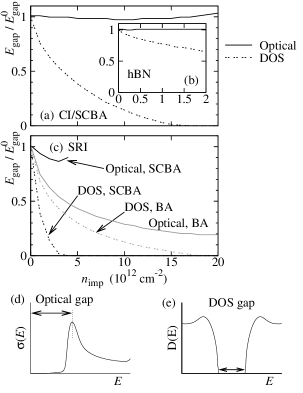
We now describe the effect of disorder on the band gap as measured by optical experiments in bilayer graphene and compare to the gap predicted by the DOS calculations. There have been several attempts to determine the band gap via measurement of the optical conductivity in absorption or reflection measurementszhang-nature2009 ; li-prl2009 ; kuzmenko-prb2009 ; mak-prl2009 . Figure 4(i) shows the transitions in the intrinsic case. The transition between the low-energy valence and conduction bands is labeled as transition 1. This transition gives a very clear peak in the optical conductivity, and since there is no Drude peak in the intrinsic case, it serves as a clear way to define the band gap. The onset of the peak occurs at in the clean limit, and therefore serves as the definition of the gap in this case. This definition is shown schematically in Fig. 5(d). Figure 4(j) shows the transitions in the extrinsic case, and we refer to this sketch in order to explain the procedure for extracting the gap. The direct transition between the low-energy conduction and valence bands [labeled transition 1 in Fig. 4(j)] is problematic for the extraction of the gap because the energy of the transition is Fermi-blocked for the lowest energy excitations and therefore does not directly give the band gap. Some experimentsmak-prl2009 instead computed the gap as the difference in energy between transition 2b and transition 3, but this is also unreliable since even a small amount of disorder masks the intricate structure of the optical conductivity. Other experiments zhang-nature2009 ; kuzmenko-prb2009 fit single particle theory with phenomenological disorder broadening to the experimental data, and while this procedure is more reliable than identifying particular peaks with individual transitions, it cannot take into account the specifics of the impurity-electron interaction, particularly at the band edge. For the purposes of the following discussion, we define the energy of the optical band gap as the top of the first peak in the optical conductivity in the intrinsic case, as indicated in Fig. 5(d). Figure 5(a) shows that this point is very robust against disorder for the CI in the SCBA [compare to the position of the top of the peak in Fig. 4(b)]. The peak in the BA moves to lower energy with disorder, implying that the measured optical gap in this approximation is not robust compared with SCBA. Similarly, the short-range interaction for the SCBA leads to such strong modification of the peak structure that it is difficult to define the optical band gap at significant impurity concentration. This information is shown in Fig. 5(a) where the optical band gap is plotted as a function of impurity density. In the main panel, a SiO2 substrate is assumed. The solid lines denote the optical gap, and we see that for the CI in the SCBA [solid black line in Fig. 5(a)], the gap does not close. In contrast, for the SRI [solid black line in Fig. 5(b)] it is only possible to define the band gap for a small range of impurity concentration, and the SRI in the BA [solid gray line in Fig. 5(b)] decreases rapidly.
We compare this to the DOS gap, which we define as the energy difference between the onset of the DOS associated with the conduction and valence bands as sketched in Fig. 5(e). This is plotted in Fig. 5(a,b) using the dashed lines as labeled in each plot. It is clear that the effect of disorder is to rapidly shrink the size of the DOS gap in all approximations. For reference, we point out that using very high quality substrates, such as hexagonal boron nitride (h-BN) dean-natnano2010 ; dassarma-prb2011 , where the impurity concentration is up to an order of magnitude smaller than in SiO2 substrates, the difference between the optical and DOS gaps defined above will be significantly smaller. This is demonstrated in the inset to Fig. 5(a), where the optical and DOS gaps for bilayer graphene on h-BN are plotted for the CI in the SCBA, for a reduced range of impurity density.
VI Summary and conclusion
In summary, we have investigated the effect of scattering from charged impurities and short-range potentials on the self-energy, density of states, and optical conductivity in gapped bilayer graphene using both the Born approximation and the self-consistent Born approximation. We have demonstrated that these two approximations give qualitatively different results for the DOS at the band edge, where the SCBA predicts that the divergence of the DOS seen in the clean limit and in the BA will be rounded off. Both approximations for the self-energy yield a DOS where the gap between the conduction and valence bands closes with increasing disorder strength. The main differences between the CI and the SRI occur at the onset of the split bands. For our choices of parameters, the SRIs are stronger at these energies and therefore the shift in the band is larger than for CI. We also introduced a self-consistent procedure to provide a computationally advantageous approximation for the low-energy properties in the CI via the SRI. We then demonstrated that the optical conductivity in the presence of disorder is a highly complicated function, the qualitative features of which depend crucially on the disorder. Our two main conclusions are that even a small level of disorder is sufficient to blur the main features of the optical conductivity of extrinsic graphene, and this makes the determination of the band gap via this measurement highly problematic. In contrast, the peak associated with the interband transition of the optical conductivity in the intrinsic case is rather robust against the effects of disorder in the CI/SCBA case. Finally, we discussed the evolution of the band gap in the DOS and extracted from optical measurements of intrinsic bilayer graphene as a function of impurity density, finding that the DOS gap is quickly reduced with increasing disorder, and eventually will be closed completely. In contrast, the gap extracted from the optical conductivity of intrinsic bilayer graphene in the SCBA is much more robust against disorder. This finding, that the DOS gap is always substantially smaller than the nominal optical gap (see Fig. 5) defined operationally for gapped BLG in the presence of disorder, may provide an explanation for why the experimental transport gap extracted for gapped BLG appears to be substantially smaller than both the theoretical single particle band gap and the experimentally extracted optical gap zhang-nature2009 ; kuzmenko-prb2009 ; li-prl2009 ; mak-prl2009 ; oostinga-natmat2007 ; zou-prb2010 ; xiao-prb2010 ; yan-nl2010 ; xia-nl2010 ; taychatanapat-prl2010 . Our results clearly indicate that this discrepancy between transport and optical gaps should disappear in systems with very little disorder such as high mobility suspended graphene or high quality graphene on h-BN substrates. It is also interesting to note that our conclusion regaring the large difference between transport and single particle (or optical) gaps is completely consistent with a recent theoretical conclusion based on percolation considerations of BLG graphene in the presence of electron-hole puddlesrossi-arXiv .
We thank US-ONR and NRI-SWAN for support.
Appendix A Approximation of Coulomb scattering by short-range scattering


In this appendix, we discuss a method for approximating the low-energy properties of the CI using the SRI. The physical mechanisms of the SRI and the CI are not related to each other since different types of disorder in the environment of the graphene will lead to each. However, as we have shown in this paper, the SRI and CI give qualitatively similar behavior for the physical observables such as the optical conductivity. If one is interested in transport characteristics, the compressibility of the electron liquid, or other quantities that depend on the carrier density, the CI is a much more time-consuming approximation to use because the screening properties vary with the carrier density and hence the self-energies also depend on it. This implies that the SCBA procedure must be implemented for every value of . This is not the case for the SRI, where the impurity interaction is constant with and so one self-energy function is valid for all carrier densities. Therefore, it would be advantageous if we could describe a method for approximating the CI by suitable choices of parameters for the SRI. In this appendix, we denote the value of set with reference to the CI by the notation . The obvious method for doing this is to set
which is still a function of via the screening wave vector. If this function is reasonably flat then a suitable constant value can be chosen as an approximation and this step removes the dependence on from the self-energy. The dashed lines in Fig. 6 (labeled ‘non-renormalized’ in the legend) show this for and . We see that for higher carrier density () there are no sharp changes in the value of determined by this method, and that the slope is relatively modest. However, at low carrier density in the gapped case, the interaction strength becomes small and this approximation will not work.
A further sophistication can be introduced to account for the effects of disorder on the density of states and hence on . In this approach, the disordered DOS is computed in the BA using the value of obtained above, and the renormalized Fermi energy is extracted by solving
where we assume that the disorder does not change the carrier density. This Fermi energy and DOS function can be used to set a new value of , and this procedure is iterated until convergence is reached for . Doing this for two disorder concentrations in the gapped and gapless cases are given in Figs. 6(a,b). These plots show that selecting will be a reasonable approximation for higher carrier density. In Figs. 6(c,d) we show a comparison of the density of states near the band edge in the SCBA for the SRI and CI for and two values of the impurity concentration. When we take and when we take . We see that the two scattering mechanisms with these parameters give almost identical results for the DOS.
Appendix B Optical conductivity
In this appendix, we present the details of the calculation of the optical conductivity in the presence of disorder. The real part of conductivity at a frequency can be calculated from the Kubo formula mahan-2000
| (11) |
where is the Fourier transform of the real-time retarded current-current correlation function defined by
| (12) |
Here is the area of the system and is the electric current operator defined by
| (13) |
where , and are creation and annihilation operators for a state , respectively.
A real-time retarded correlation function can be easily calculated from a finite-temperature correlation function through the analytic continuation in the complex space. The finite-temperature current-current correlation function is defined by
| (14) |
where is a time-ordering operator for an imaginary time , is a Matsubara frequency and .
Then the lowest-order correlation function is given by
| (15) |
where is the finite-temperature Green’s function defined by the Fourier transform of . Note that the spectral representation of is given by
| (16) |
where is a spectral weight function with . From Eqs. (15) and (16),
| (17) |
where and is the chemical potential. Here the following frequency sums for fermions at finite temperatures were used:
| (18) | |||
Through the analytic continuation of , the conductivity expression can be derived from Eqs. (11) and (17). The energy bands have rotational symmetry and by taking this into account along with the spin and valley degeneracy, we finally get the conductivity expression at zero-temperature as in Eq. (9).
References
- (1) S. Das Sarma, S. Adam, E. H. Hwang, and E. Rossi, Rev. Mod. Phys. 83, 407 (2011).
- (2) D. S. L. Abergel, V. Apalkov, J. Berashevich, K. Ziegler, and T. Chakraborty, Adv. Phys. 59, 261 (2010).
- (3) E. McCann, Phys. Rev. B. 74, 161403(R) (2006).
- (4) T. Ohta, A. Bostwick, T. Seyller, K. Horn, and E. Rotenberg, Science 313, 951 (2006).
- (5) Y. Zhang, T.-T. Tang, C. Girit, Z. Hao, M. C. Martin, A. Zettl, M. F. Crommie, Y. Ron Shen, F. Wang, Nature 459, 820 (2009).
- (6) A. B. Kuzmenko, I. Crassee, D. van der Marel, P. Blake and K. S. Novoselov, Phys. Rev. B 80 165406 (2009).
- (7) Z. Q. Li, E. A. Henriksen, Z. Jiang, Z. Hao, M. C. Martin, P. Kim, H. L. Stormer, and D. N. Basov, Phys. Rev. Lett. 102, 037403 (2009).
- (8) K. F. Mak, C. H. Lui, J. Shan, and T. F. Heinz, Phys. Rev. Lett. 102 256405 (2009).
- (9) T. Ando, A. B. Fowler and F. Stern, Rev. Mod. Phys. 54, 437 (1982).
- (10) J. B. Oostinga, H. B. Heersche, X. Liu, A. F. Morpurgo, and L. M. K. Vandersypen, Nat. Mater. 7, 151 (2007).
- (11) K. Zou and J. Zhu, Phys. Rev. B 82, 081407(R) (2010).
- (12) S. Xiao, J.-H. Chen, S. Adam, E. D. Williams, and M. S. Fuhrer, Phys. Rev. B 82, 041406 (2010).
- (13) J. Yan and M. S. Fuhrer, Nano Lett., 10, 4521 (2010).
- (14) F. Xia, D. B. Farmer, Y. Lin, and P. Avouris, Nano Lett., 10, 715 (2010).
- (15) T. Taychatanapat and P. Jarillo-Herrero, Phys. Rev. Lett. 105, 166601 (2010).
- (16) L. Jing, J. Velasco Jr., P. Kratz, G. Liu, W. Bao, M. Bockrath, and C. N. Lau, Nano Lett. 10, 4000 (2010).
- (17) For a thorough review of the effect of disorder on monolayer graphene, see in particular Ref. dassarma-rmp2011, and also E. R. Mucciolo and C. H. Lewenkopf, J. Phys.: Condens. Matter 22, 273201 (2010).
- (18) S. Das Sarma, E. Hwang and E. Rossi, Phys. Rev. B 81, 161407 (2010).
- (19) E. H. Hwang and S. Das Sarma, Phys. Rev. B 82, 081409(R) (2010).
- (20) D. S. L. Abergel, E. H. Hwang, and S. Das Sarma, Phys. Rev. B 83, 085429 (2011).
- (21) A. F. Young, C. R. Dean, I. Meric, S. Sorgenfrei, H. Ren, K. Watanabe, T. Taniguchi, J. Hone, K. L. Shepard, and P. Kim, e-print arXiv:1004.5556v2.
- (22) E. A. Henriksen and J. P. Eisenstein, Phys. Rev. B 82, 041412(R) (2010).
- (23) E. Rossi, S. Das Sarma, arXiv:1103.3012 (unpublished).
- (24) M. Koshino and T. Ando, Phys. Rev. B 73, 245403 (2006).
- (25) C. Bena, Phys. Rev. Lett. 100, 076601 (2008).
- (26) J. Nilsson, A. H. Castro Neto, F. Guinea, and N. M. R. Peres, Phys. Rev. B 78, 045405 (2008).
- (27) T. Ando, J. Phys. Soc. Jpn. 80, 014707 (2011).
- (28) A. Ferreira, J. Viana-Gomes, J. Nilsson, E. R. Mucciolo, N. M. R. Peres, and A. H. Castro Neto, Phys. Rev. B 83, 165402 (2011).
- (29) S. Yuan, H. De Raedt, M. Katsnelson, Phys. Rev. B 82, 235409 (2010).
- (30) E. V. Castro, M. P. López-Sancho, and M. A. H. Vozmediano, Phys. Rev. Lett. 104, 036802 (2010).
- (31) V. V. Mkhitaryan and M. E. Raikh, Phys. Rev. B 78, 195409 (2008).
- (32) H. P. Dahal, A. V. Balatsky, and J.-X. Zhu, Phys. Rev. B 77, 115114 (2008).
- (33) J. Nilsson and A. H. Castro Neto, Phys. Rev. Lett. 98, 126801 (2007).
- (34) H. Min, D. S. L. Abergel, E. H. Hwang, and S. Das Sarma, Phys. Rev. B 84, 041406 (2011).
- (35) E. H. Hwang and S. Das Sarma, Phys. Rev. B 75, 205418 (2007).
- (36) E. H. Hwang and S. Das Sarma, Phys. Rev. Lett. 101, 156802 (2008).
- (37) P. Blake, E. W. Hill, A. H. Castro Neto, K. S. Novoselov, D. Jiang, R. Yang, T. J. Booth, and A. K. Geim, Appl. Phys. Lett. 91, 063124 (2007).
- (38) D. S. L. Abergel, A. Russell, and V. I. Fal’ko, Appl. Phys. Lett. 91, 063125 (2007).
- (39) E. J. Nicol and J. P. Carbotte, Phys. Rev. B. 77, 155409 (2008).
- (40) H. Min and A. MacDonald, Phys. Rev. Lett. 103, 067402 (2009).
- (41) C. R. Dean, A. F. Young, I. Meric, C. Lee, L. Wang, S. Sorgenfrei, K. Watanabe, T. Taniguchi, P. Kim, K. L. Shepard, and J. Hone, Nat. Nano. 5, 722 (2010).
- (42) S. Das Sarma and E. H. Hwang, Phys. Rev. B 83, 121405(R) (2011).
- (43) G. D. Mahan, Many-Particle Physics (3rd ed.), Kluwer Academic/Plenum Publishers, New York (2000).