The Diamond SQUID
Abstract
Diamond is an electrical insulator in its natural form. However, when doped with boron above a critical level ( 0.25 at.%) it can be rendered superconducting at low temperatures with high critical fields. Here we present the realization of a micrometer scale superconducting quantum interference device (-SQUID) made from nanocrystalline boron doped diamond (BDD) films. Our results demonstrate that -SQUIDs made from superconducting diamond can be operated in magnetic fields as large as 4T independent on the field direction. This is a decisive step towards the detection of quantum motion in a diamond based nanomechanical oscillator.
Micro and nano SQUIDS01Cleziou are extremely sensitive tools for magnetization measurements on the local scale and find applications in various fields of science such as scanning SQUID microscopy02Kirtley . However, the present state of the art limits its utility to magnetic fields well below a tesla. Even though, several attempts to realize micrometer scale superconducting quantum interference devices (-SQUIDs) form materials with high critical field such as Nb3Sn 2aWu or Nb3Ge 2bDilorio ; 2cRogalla have been realized, the demonstration of a device remaining operational at high magnetic fields has been elusive to date. In this context, diamond, when doped with boron above a critical level ( 0.25 at.%) which results in a superconductor with very high critical field07Takano is an extremely promising material. In addition, recent advances in diamond thin film growth technology have paved the way toward large scale processing of high quality devices.This recently discovered material not only enables us to make -SQUIDs capable of operating at fields as high as 4T independent of the field direction, as reported in this paper, but also finds a potential application for ultra-sensitive motion detection of diamond based nanomechanical systems05Etaki .
The discovery of superconductivity in diamond03Ekimov ; 04Blase ; 06Nesladek ; 07Takano has opened the possibility to combine outstanding mechanical properties with superconductivity. Diamond is the archetype of superhard materials with the highest Young’s modulus08Dubitskiy ; 09Willchemphy . The main interest in such super-hard superconducting materials comes from their possible application to high frequency nanomechanical systems. This high stiffness and the reduced mass of nanomechanical structures made out of diamond enable GHz vibration frequencies comparable with or higher than thermal energies at milliKelvin temperatures10Gaidarzhy . This opens the possibility of studying the quantum regime of such nanomechanical resonators11Cleland ; 11aTeufel1 ; 11bTeufel2 .
Advances in nanofabrication technology have made it possible to realise complex devices involving nano-electromechanical components12Naik ; 13Knobel . But in most cases the nano-mechanical devices are compound/hybrid devices consisting of a super-hard component with high Young’s modulus generating high frequency resonators, and of a conducting component to reduce the transmission losses of the system. However, this conductive component decreases the mechanical rigidity and thus reduces the overall quality factor of the device. In this context, boron doped diamond turns out to be an excellent candidate for fabricating monolithic superconducting circuits involving nanomechanical systems with very high quality factor. One can then envision the direct integration of such nanomechanical systems into superconducting circuits such as SQUIDs05Etaki or superconducting resonators14regal for ultra sensitive motion detection.
Results and Discussions
As a first step in this direction, we fabricated diamond -SQUIDS patterned from a 300 nm thick superconducting nano-crystalline diamond film. The boron doped diamond films were grown by microwave plasma enhanced chemical vapour deposition (MWPECVD) on seeded silicon 100 wafers with a silica buffer layer of 500 nm15Williams . The thickness was monitored in situ with laser interferometry. The growth process has been discussed in detail elsewhere16Williams . The diamond thin films were patterned using standard electron beam lithography. A thin nickel mask (65 nm) was deposited for subsequent highly anisotropic oxygen plasma etching17Mandal . Titanium-platinum-gold was deposited for the contact pads (figure 1a) and the sample was annealed at 750o C to ensure good ohmic properties.
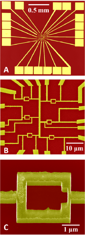
We fabricated several similar devices as depicted in figure 1 with various weak link designs of width of 250 nm, 170 nm and 100 nm. These weak links serve as the Josephson junctions in the superconducting loop17aDayem ; 17bLikharev . Here we mainly discuss data measured on a -SQUID with an area of 2.5m 2.5m with two symmetric weak links (100 nm wide if not stated otherwise). Our low field measurements were performed in a 3He closed cycle refrigerator with a base temperature of 400 mK, whereas the high field measurements have been undertaken in a dilution refrigerator at a temperature of 40 mK. The superconducting critical temperature of the bulk as well as the nanostructured diamond film was about 3K as shown in figure 2a.
The general characteristics of our -SQUIDS have been summarized in figure 2.
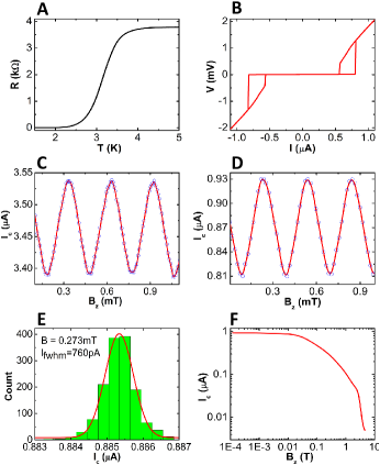
The current voltage (I-V) characteristic shows a thermal hysteresis18aSkocpol ; 18Courtois with a critical current of almost 1A and a retrapping current of about 0.55A. These parameters can be changed by tuning the geometrical aspects of the weak link. To demonstrate the performance of our diamond -SQUIDs we have measured the critical current oscillation as a function of perpendicular magnetic field. At low magnetic field we swept the current from a value slightly below the retrapping current until the switching of the SQUID was detected and recorded. This was repeated for different magnetic fields. The results for these experiments are shown in figure 2c and d. An oscillation period of approximately 3.1 G was recorded which corresponds to an effective SQUID surface area of 2.6 2.6 m2, in agreement with the geometrical dimensions of the -SQUID. The resulting modulation amplitude was about 15% for 100 nm wide weak links and around 5% for a 250 nm width comparable to what is observed for Al and Nb -SQUIDs18aHasselbach . To probe the sensitivity of our -SQUID we repeated current switching measurements at a fixed magnetic field. Taking the full width at half maximum and taking into account the sampling frequency we obtained a sensitivity of , where is the superconducting flux quantum. This sensitivity is comparable to similarly designed -SQUIDS from frequently employed superconductors such as niobium or aluminium19Hasselbach but a careful optimization of the SQUID design as well as material can lead to much higher sensitivities19aVoss . At present the sensitivity is only limited by the electronic measurement set-up or external noise as the histograms are still symmetric and not limited by quantum fluctuations even at 40 mK. The main advantage of the diamond system is that superconductivity persists up to very high magnetic field (in our case more than 4 T). This is shown by the field dependence of the critical current as depicted in figure 2f.
Various types of -SQUIDs have been reported in the literature, which are extremely sensitive magnetic flux detectors and currently used for scanning SQUID microscopy01Cleziou ; 19Hasselbach , magnetization measurements in mesoscopic systems19bRabaud ; 20Bluhm and in isolated molecules21Wernsdorfer . However, a severe drawback of these detectors is the narrow field range in which they are operable. In particular, -SQUID devices were operated at fields above 1 T only when the field is applied perfectly in the plane of the SQUID22chen . In addition, in such a parallel field configuration, the thickness of the superconducting layer has to be extremely small (of the order of few nanometers), a feature which drastically reduces the critical current. On the other hand, operating standard -SQUIDs in perpendicular field reduces severely the operational field range well below 1T. Here we demonstrate that -SQUIDs made from boron doped diamond do not suffer from such limitations and can be operated in magnetic fields as high as 4 T even when applied in perpendicular configuration. This is more than a six-fold increase on the present state of the art23Finkler .
In figure 3c-f
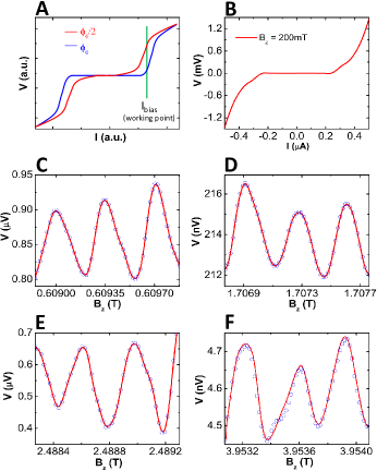
we have shown the characteristic SQUID oscillations at various fields up to 4 T. The oscillations are not perfectly periodic due to the fact that we had to use the z-coil (perpendicular to SQUID plane) for both, to apply the steady magnetic field (up to 4 T) and also to probe the SQUID oscillations (of the order of 0.3 mT). The field resolution is hence limited by the resolution of the magnet power supply ( 0.1 mT). This could be improved by adding an additional feed line next to the -SQUID to probe the SQUID oscillations independently05Etaki .
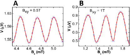
In order to demonstrate the insensitivity of our SQUID to the applied field direction we have also measured SQUID oscillations by applying a constant field with a vector magnet in the x-y plane (parallel to SQUID plane). In this configuration the SQUID oscillations were probed using a small magnetic field of a few milli Teslas in the z-coil. The voltage oscillations for a parallel field of 0.5 and 1 T, the maximal field achievable with our vector coil, are shown in figure 4.
Let us also emphasize that these oscillations were obtained for 300 nm thick superconducting boron doped diamond layers. In this case the aspect ratio is very favorable for vortex penetration, and in standard superconductors, current oscillations are usually not observed in -SQUIDS for layers thicker than a few nanometers. The fact that we are able to observe SQUID oscillations for such geometries may originate from the granularity of the material24Dahlem , which favors vortex pinning.
Let us mention that the resulting SQUID oscillations at high magnetic field have not been optimized at each field and for this reason the oscillation amplitude does not follow the field strength. Here we simply demonstrate the proof of principle that a diamond SQUID can be operated at high magnetic field and this independent on the field direction. In order to optimize the sensitivity of the diamond SQUID it would be extremely interesting to employ single crystal diamond where higher critical currents25Watanabe as well as higher critical fields (10T)07Takano can be achieved.
SQUID oscillations surviving at high magnetic fields, independent of field orientation, open the possibility to exploit these exceptional properties for HF magnetic surface probe techniques02Kirtley . Combining these exceptional superconducting and outstanding mechanical properties makes this monolithic system a highly promising tool, in particular for the detection of quantum motion in a diamond based nanomechanical oscillator when inserted within one arm of a diamond SQUID05Etaki .
Methods
Film Deposition
Prior to deposition, the wafers were cleaned by standard RCA SC1 solution and rinsed with deionized water in an ultrasonic bath. Immediately after rinsing the wafers were immersed in a colloid of mono-disperse diamond nano-particles known to have a mean size of 6 nm, and agitated by ultrasound for 30 min. Following this seeding process, the wafers were rinsed again with deionized water, blown dry in nitrogen and immediately placed inside the growth chamber which was pumped down to a vacuum lower than 10-6 mbar. The chamber was then purged with hydrogen gas and a plasma ignited with 4% methane and 6500 ppm of tri-methylboron diluted by hydrogen (better than 99.9999999% pure). The pressure was ramped to 50 mbar and the temperature was 700o C as measured by optical pyrometry.
Electronic Measurements
The SQUID measurements have been performed by current biasing the squid loop via a thermostable 1 M resistor using a 16 bit NI-USB-6229 DAC. At low magnetic field, the I-V characteristic is hysteretic as seen in figure 2b and the SQUID oscillation is measured by recording the critical current as a function of magnetic field. The critical current is determined when a voltage drop is generated across the SQUID due to its transition from the superconducting to the normal state. The voltage is amplified with a NF-LI75a low-noise voltage amplifier and recorded via a Keithley 2000 Multimeter. The SQUID oscillations shown in figure 2 are obtained with a single I-V curve at a fixed magnetic field. No averaging has been done.
Applying a large magnetic field (B500 mT) to a superconductor reduces the critical current. When the reduction of the critical current is below the value of the retrapping current, the voltage-current characteristics become non-hysteretic as shown in figure 3b. In this case, an ac measurement technique can be used to measure the SQUID oscillations. The SQUID is biased with a square wave signal by mixing a sinusoidal voltage (amplitude of 1 V and a frequency of 11.7 Hz) with the dc voltage of the NI-DAC. The voltage generated across the SQUID is amplified with a home-made ultra-low noise voltage amplifier (0.5nV/) and measured with a Lock-In amplifier (Signal recovery 7265). An I-V curve measured with this technique is displayed in figure 3b. By adjusting the DC voltage of the DAC, the bias current IB can then be set at the working point of the SQUID (see figure 3A). Sweeping the magnetic field at fixed bias current results in voltage oscillations as shown in figures 3c-f and 4a,b.
Acknowledgements
We would like to acknowledge technical assistance from the Nanofab team of the Institut Néel, in particular B. Fernandez. We also acknowledge valuable discussions with Wolfgang Wernsdorfer, Klaus Hasselbach and Vincent Bouchiat and technical assistance from Y. Baines. This work has been supported by the French National Agency (ANR) in the frame of its program in “Nanosciences and Nanotechnologies” (SUPERNEMS Project no. ANR-08-NANO-033). This work was partially supported by the Fraunhofer Attract award “Hybrid HF-MEMS Filters for GHz-Communication and capillary MEMS systems for chemical and bio-chemical Sensing - COMBIO”.
References
- (1) Cleuziou, J.-P.; Wernsdorfer, W.; Bouchiat, V.; Ondar uhu, T.; Monthioux, M. Nature Nanotechnology 2006, 1, 53.
- (2) Kirtley, J. R.; Tsuei, C. C.; Sun, J. Z.; Chi, C. C.; Yu-Jahnes, Lock See; Gupta, A.; Rupp, M.; Ketchen, M. B. Nature 1995, 373, 225.
- (3) Wu, C. T.; Falco, C. M. Appl. Phys. Lett 1977, 30, 609.
- (4) Dilorio, M.S.; de Lozanne, A.; Beasley, M. R. IEEE Trans. Mag. 1983, 19, 308.
- (5) Rogalla, H.; David, B.; Rühl, J. J. Appl. Phys. 1984, 55, 3441.
- (6) Takano, Y. J. Phys.: Condens. Matter 2009, 21, 253201.
- (7) Etaki, S.; Poot, M.; Mahboob, I.; Onomitsu, K.; Yamaguchi, H.; van der Zant, H. S. J. Nature Physics 2008, 4, 785.
- (8) Ekimov, E.A.; Sidorov, A.A.;Bauer, E.D.; Mel’nik, N.N.; Curro, N.J.; Thompson, J.D.; Stishov, S.M. Nature 2004, 428, 542.
- (9) Blase, X.; Bustarret, E.; Chapelier, C.; Klein, T.; Marcenat, C. Nature Materials 2009, 8, 375.
- (10) Nesladek, M.; Tromson, D.; Mer, C.; Bergonzo, P.; Hubik, P.; Mares, J.J. Appl. Phys. Lett. 2006, 88, 232111.
- (11) Dubitskiy, G. A.; Blank, V. D.; Buga, S. G.; Semenova, E. E.; Kul’bachinskii, V. A.; Krechetov, A. V.; Kytin, V. G. JETP Lett. 2005, 81, 260.
- (12) Williams, O.A.; Kriele, A.; Hees, J.; Wolfer, M.; M ller-Sebert, W.; Nebel, C.E. Chem. Phys. Lett. 2010 495, 84.
- (13) Gaidarzhy, A.; Imboden, M.; Mohanty, P.; Rankin, J.; Sheldon, B. W. Appl. Phys. Lett. 2007, 91, 203503.
- (14) O’Connell, A. D.; Hofheinz, M.; Ansmann, M.; Bialczak, R. C.; Lenander, M.; Lucero, E.; Neeley, M.; Sank, D.; Wang, H.; Weides, M.; Wenner, J.; Martinis, J. M.; Cleland, A. N. Nature 2010, 464, 697.
- (15) Teufel, J. D.; Li, D.; Allman, M. S.; Cicak, K.; Sirois, A. J.; Whittaker, J. D.; Simmonds, R. W. Nature, 2011, 471, 204.
- (16) Teufel, J. D.; Donner, T.; Li, D.; Harlow, J. W.; Allman, M. S.; Cicak, K.; Sirois, A. J.; Whittaker, J. D.; Lehnert, K. W.; Simmonds, R. W. arXiv:1103.2144v1 2011
- (17) Naik, A.; Buu, O.; LaHaye, M. D.; Armour, A. D.; Clerk, A. A.; Blencowe, M. P.; Schwab, K. C. Nature 2006, 443, 193.
- (18) Knobel, R. G.; Cleland, A. N. Nature 2003, 424, 291.
- (19) Regal, C. A.; Teufel, J. D.; Lehnert, K. W. Nature Physics 2008, 4, 555.
- (20) Williams, O.A.; Douheret, O.; Daenen, M.; Haenen, K.; Osawa, E.; Takahashi, M. Chem. Phys. Lett. 2007, 445, 255.
- (21) Williams, O.A.; Nesladek, M.; Daenen, M.; Michaelson, S.; Hoffman, A.; Osawa, E.; Haenen, K.; Jackman, R.B. Diamond and Related Materials 2008, 17, 1080.
- (22) Mandal, S.; Naud, C.; Williams, O. A.; Bustarret, E.; Omnès, F.; Rodière, P.; Meunier, T.; Saminadayar, L.; Bäuerle, C. Nanotechnology 2010, 21, 195303.
- (23) Anderson, P. W.; Dayem, A. H. Phys. Rev. Lett. 1964, 13, 195-197.
- (24) Likharev, K. K. Rev. Mod. Phys. 1979, 51, 101-159.
- (25) Skocpol, W. J. Phys. Rev. B 1976, 14, 1045.
- (26) Courtois, H.; Meschke, M.; Peltonen, J. T.; Pekola, J. P. Phys. Rev. Lett. 2008, 101, 067002.
- (27) Hasselbach, K.; Mailly, D.; Kirtley, J. R. J. Appl. Phys. 2002, 91, 4432-4437.
- (28) Hasselbach, K.; Veauvy, C.; Mailly, D. Physica C 2000, 332, 140.
- (29) Voss, R. F.; Laibowitz, R. B.; Broers, A. N.; Raider, S. I.; Knoedler, C. M.; Viggiano, J. M. IEEE Trans. Mag. 1981, 17, 395.
- (30) Rabaud, W.; Saminadayar, L.; Mailly, D.; Hasselbach, K.; Benoît, A.; Etienne, B. Phys. Rev. Lett. 2001, 86 3124-3127.
- (31) Bluhm, H.; Koshnick, N. C.; Bert, J. A.; Huber, M. E.; Moler, K. A, Phys. Rev. Lett. 2009, 102 136802.
- (32) Wernsdorfer, W.; Sessoli, R. Science 1999, 284, 133.
- (33) Chen, L.; Wernsdorfer, W.; Lampropoulos, C.; Christou, G.; Chiorescu, I. Nanotechnology 2010, 21, 405504.
- (34) Finkler, A.; Segev, Y.; Myasoedov, Y.; Rappaport, M. L.; Ne’eman, L.; Vasyukov, D.; Zeldov, E.; Huber, M. E.; Martin, J.; Yacoby, A. Nano Letters 2010, 10, 1046.
- (35) Dahlem, F.; Achatz, P.; Williams, O.A.; Araujo, D.; Bustarret, E.; Courtois, H. Phys. Rev. B 2010, 82, 033306.
- (36) Watanabe, M.; Kawano, A.; Kitagoh, S.; Yamaguchi, T.; Takano, Y.; Kawarada, H. Physica C 2010, 470, S613.