Large local Hall effect in pin-hole dominated multigraphene spin-valves.
Abstract
We report local and non-local measurements in pin-hole dominated mesoscopic multigraphene spin-valves. Local spin-valve measurements show spurious switching behavior in resistance during magnetic field sweeping similar to the signal observed due to spin-injection into multigraphene. The switching behavior has been explained in terms of local Hall effect due to thickness irregularity of the tunnel barrier. Local Hall effect appears due to large local magnetostatic field produced at the roughness in the AlOx tunnel barrier. The effect of this local Hall effect is found to reduce as temperature is increased above 75 K. The strong local Hall effect hinders spin-injection into multigraphene resulting in no spin signal in non-local measurements.
pacs:
XX-XX, XX-XX-XXI Introduction
Graphene and few-layer graphene has shown to be ideal material for spintronics devices because of suppressed hyperfine interaction and weak spin-orbit couplinghernando . Gate tunable conductivity along with low carrier density ( 1012 cm-2) and high mobility ( 104 cm2V-1s-1) gives opportunity to fabricate ultra-fast spintronic devices with this materialgeim . Efficient spin-polarized carrier injection into graphene is one of the essential requirements for such devices. Significant improvement has been achieved in this direction through successful demonstration of spin injection into single and few-layer graphene (also called multigraphene) at room temperature by different groups tombrosnature ; hill ; cho ; nishioka ; wang ; jo ; goto ; tb . Long spin diffusion length 2 m and spin life time 50-200 ps have been reported in single layer graphene through spin injection experimentstombrosnature . Much longer spin life time 2 ns has been observed in bilayer graphenehan ; yang . Few-layer graphene is now believed to be a more appropriate candidate for spin injection compared to single layer graphene because of the screening of scattering potentials from substrate in the formermassen ; yang ; garcia . However, experimental values of and are still an order of magnitude shorter than what is expected theoreticallyhernando . Therefore, an efficient engineering of spin-valve devices is required to realize the full potential of multigraphene spintronics devices.
Spin-valve devices for spin injection show high to low resistance switching, which depends on the relative magnetization of the two ferromagnetic electrodes. Spin polarized carriers are injected from one ferromagnet (injector) and the probability of these carriers to be collected at the other ferromagnet (detector) depends on the magnetization of the latter. Therefore, quality of interface between the ferromagnet and graphene may significantly affect the spin-polarized carrier injection into graphene. A proper understanding of the micromagnetic phenomena occurring at the interface is essential for the optimization of such devices. In order to avoid conventional Schottky barrier contact due to the large conductivity mismatch between graphene and the metallic ferromagnet, a tunneling approach has been suggestedhanprl ; jozsa . However, conventional tunnel barriers suffer from complications like pin-holes and nonuniform barrier thickness. These defects in the barrier give additional features by contributions from anisotropic magnetoresistance (AMR) and local Hall effect that obscure spin injection signalhong . In particular, stray magnetostatic fields produced at the interface due to the ferromagnet on top of it may have significant impact. Recently, spin precession and inverted Hanle effect has been reported in Si spin injection devices which arise from local magnetostatic fields at tunnel barrier roughnessdas .
In this work, we demonstrate large local Hall effects due to stray magnetostatic fields at the tunnel barrier roughness in multigraphene spin-valves. We observe resistance switching behavior due to this local Hall effect. We found that spin injection is strongly hindered by the presence of these stray magnetostatic fields. No resistance switching was observed in non-local measurements due to this.
II Fabrication and experimental details
Multigraphene samples were prepared on Si/Si3N4 substrate by rubbing small flake of highly oriented pyrolytic graphite (HOPG) from Advanced Ceramics (grade ZYA, rocking curve 0.4o). Thickness of the multigraphene flakes were measured using atomic force microscope (AFM). For device fabrication 30 nm thick and 10 m long multigraphene samples were chosen. Spin-valve devices were fabricated by conventional electron beam lithography method. Thermally evaporated Al on top of multigraphene was oxidized to form AlOx tunnel barrier. The thickness of the AlOx tunnel barrier was found out to be 2 nm from AFM measurements. For spin polarized carrier injection into multigraphene 50 nm thick Co was thermally evaporated on a pre-patterned structure of PMMA prepared by electron beam lithography. Ferromagnetic Co lines of different width (as shown in Fig. 1) were patterned using this technique. Different width of Co was used to ensure different coercive fields between electrodes. The distance between two inner Co electrode (l) was varied from 1-3 m for different spin-valve devices. A thin layer of Pt was immediately evaporated on top of Co to prevent it from oxidation. The Co lines were further contacted to larger contact pads through gold lines. Magnetoresistance measurements were done in a closed cycle refrigerator using an AC resistance bridge. For spin valve measurements magnetic field was applied in the plane of the film along the long axis of the Co line using an electromagnet with rotation option.
III Results and discussion
Temperature dependence of resistance of the spin-valve device showed a semiconducting behavior as typically observed for multigraphene samples reported elsewherearndt ; garcianjp . Current-Voltage (IV) characteristics were measured on as fabricated samples at room temperature and 15 K. Spin-valve devices showed slightly nonlinear IV with few kOhm resistance due to the presence of AlOx tunnel barrier. However, with repeated IV measurement with maximum current up to 10 A the devices showed linear IV with resistance decreasing down to 435 Ohm at 15 K. The rapid decrease of resistance with linear IV can be understood by considering formation of pin-holes during the measurement process. The resistance of the spin-valves was measured with an AC resistance bridge with 1.5 A current limit range.
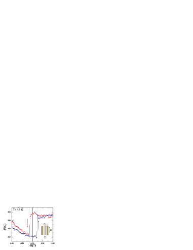
Fig. 2 shows the field dependence of the resistance of one of the spin-valve device measured at 15 K. The measurement configuration called local configuration is shown in the inset of Fig. 2. Magnetic field () is applied along the long axis of the Co line. Resistance switching can be seen at a magnetic field 0.1 T. The resistance switches from higher resistance to a lower resistance while field is swept from +0.5 T to -0.5 T. A reverse case happens while field is swept from -0.5 T to +0.5 T. The direction of field sweeping is shown by arrows in the figure.
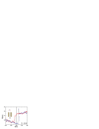
Fig. 3 shows a similar resistance switching behavior for a 3-terminal local configuration as shown in the inset. Our resistance switching behavior is significantly different from resistance switching seen in local measurements in graphene spin injection devices reported in literaturetombrosnature ; han . In spin injection devices step-like switching is seen for parallel and antiparallel orientation of the ferromagnetic electrodes. High resistance state is achieved for antiparallel configuration of inner two electrodes and a low resistance for parallel configuration. Our switching behavior is quite unusual and can be misunderstood as signature of spin injection.
The observed switching behavior can be understood by considering the presence of different stray magnetostatic fields in the spin-valve device. Magnetostatic fields in a spin-valve device appears mainly from two sources: (1) Fringe magnetostatic fields at the edges of the ferromagnetic electrodes monzon and (2) Magnetostatic fields near the multigraphene and ferromagnet (Co) interface due to finite roughness of the tunnel barrierdas .With the magnetic field applied along the long axis of the Co electrode fringe fields from the edges can be ignored in our spin-valves as the long edges of the Co electrode lie far from the multigraphene (see Fig. 1). Most of the magnetostatic fields in our device mainly originate from the AlOx roughness. As we observe a linear IV characteristics, the AlOx tunnel barrier in our spin-valve is highly nonuniform with a lot of pin-holes. So when the ferromagnetic Co electrode is magnetized due to roughness of the oxide barrier, a local magnetostatic field with a strong normal component can be generated. In a very simplified situation with one dimensional periodic roughness along axis the magnetostatic field generated from a ferromagnet with magnetization pointing along the direction can be written asdas ; nogaret ,
| (1) |
. Where and
| (2) |
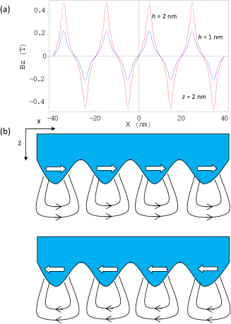
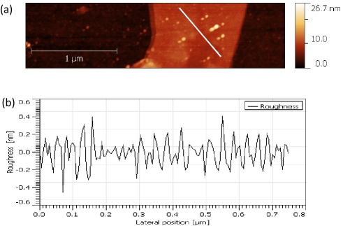
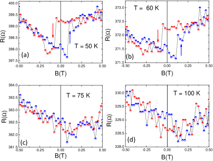
Here is the peak-to-peak roughness height and the period of the roughness profile of the barrier. To get a detailed idea about the roughness of AlOx tunnel barrier we performed AFM measurements of our spin valve as shown in Fig. 4(a). Roughness profile of AlOx on top of multigraphene along the marked line in Fig. 4(a) is shown in Fig. 4(b). Note that in our spin-valves multigrphene is covered with AlOx all over it before patterning the Co electrodes. Clearly, the roughness amplitude in the AlOx layer is 1 nm. However, considering the linear IV characteristics and the possibility to have pin-holes we can assume a maximum roughness amplitude 2 nm i.e, of the order of the thickness of the AlOx barrier. For ferromagnetic Co with T, and assuming 20 nm the out of plane component of magnetic field () calculated using Eq. (1) at = 2 nm is shown in Fig. 5 (a) for = 1 and 2 nm, respectively. The local magnetostatic fields can be as large as 0.45 T. A pictorial representation of the stray magnetostatic fields for a sinusoidal roughness of the tunnel barrier is shown in Fig. 5 (b) with magnetization pointing in two opposite direction. Therefore, when an external field 0.1 T is applied to saturate the Co electrode, the multigraphene with a tunnel barrier roughness 2 nm can experience much higher field of the order of 0.45 T in local areas. We believe these stray magnetostatic fields will provide additional voltage contribution to the measured longitudinal voltage . The value of will depend on the actual distribution of the stray magnetostatic fields, and therefore on the roughness. However, in a more qualitative way one can say that in a mesoscopic device with irregular geometry voltage between any two points can be written as a linear combination of longitudinal () and Hall () voltages . Therefore, one can write, , where and are sample dependent constants. When the magnetization of Co electrode changes direction the perpendicular component of the magnetostatic field , changes sign resulting in change in the sign of Hall voltage . Therefore, the measured voltage , for , pointing upward, can be written as,, and in this case one gets a high resistance state. Similarly, for pointing downwards one can write, and thus a low resistance state is achieved. The switching from the high resistance to low resistance state occurs at a magnetic field when magnetization of the Co electrode changes, i.e, at the coercive field of the inner Co electrode. Although one expects two resistance switching corresponding to the magnetization switching of the two inner Co electrodes, we found only one resistance switching probably because the narrower Co electrode produces too small resistance change to be observable within our experimental resolution. We also measured our spin-valves at different temperatures and we found that the resistance change produced by this local Hall effect becomes too small and in the range of experimental noise above 75 K. Field dependence of resistance measured at T = 50, 60, 75 and 100 K in the local configuration (see Fig. 2) is shown in Fig. 6.
Another possible source of switching in resistance in spin-valves can come from anisotropic magnetoresistance (AMR) of the Co electrodesfilip . However, we could not find any sharp resistance switching in spin-valves with Co electrodes without any AlOx tunnel barrierheuse . Therefore, we believe the sharp resistance switching in our spin-valves is mainly due to local Hall effect.
Clear signature of spin injection into multigraphene is usually seen in non-local measurements in a configuration as shown in the inset of Fig. 7. In this configuration, electrical charge current path is completely separated from spin current path so that signals only due to spin current can be observed. In our devices, we could not find any switching in resistance in non-local measurement done at 15 K with voltage pads placed 1.5 m away from the current path. We believe the local Hall effect due to tunnel barrier roughness significantly suppress spin injection into multigraphene. Although, there might be additional reasons for the absence of non-local signal in our spin-valves, we believe that local magnetostatic fields at the tunnel barrier roughness definitely plays a role in spin-injection. Therefore, for a clear observation of resistance changes due to spin injection into multigraphene full coverage of spin-transport channel with a smooth tunnel barrier is essential.
IV Conclusions
In summary, we have fabricated submicron spin-valve devices with few-layer graphene of different thickness. Our spin-valves showed resistance switching behavior at low temperatures in local measurement configuration. However, in non-local configuration we could not see any switching indicating reduced spin injection. The switching behavior in local measurement can be qualitatively understood in terms of large local Hall effect. The local Hall effect appears due to magnetostatic fields present in the device. We estimated that for a roughness 2 nm the local magnetostatic fields can be as large as 0.45 T. Local Hall effect can result in spurious resistance switchings, which can be confused with resistance switching due to spin injection into spin valve systems. Pin-hole free smooth barriers along with narrow ferromagnetic electrodes are prerequisite for spin-injection into multigraphene.
Acknowledgements.
This research has been supported by grants from Deutsche Forschungsgemeinschaft under Contract No. DFG ES 86/16-1.SD and AB acknowledge financial support by Graduate School of Natural Sciences BuildMoNa of the University of Leipzig.References
- (1) Huertas-Hernando D, Guinea F and Brataas A 2006 Phys. Rev. B 74 155426
- (2) Geim A K and Novoselov K S 2007 Nature Mater. 6, 183 191
- (3) Tombros N, Jozsa C, Popinciuc M, Jonkman H T and Van Wees B J 2007 Nature 448 571
- (4) Hill E W, Geim A K, Novoselov K, Schedin F and Blake P 2006 IEEE Trans. Magn. 42 2694
- (5) S Cho, Y-F Chen and Fuhre M S 2007 Appl. Phys. Lett. 91 123105
- (6) Nishioka M and Goldman A M 2007 Appl. Phys. Lett. 90 252505
- (7) Wang W H, Pi K, Li Y, Chiang Y F, Wei P, Shi J and Kawakami R K 2008 Phys. Rev. B 77 020402
- (8) Sanghyun Jo, Dong-Keun Ki, Dongchan Jeong, Hu-Jong Lee, and Stefan Kettemann 2011 Phys. Rev. B 84 075453
- (9) Goto H, Kanda A, Sato T, Tanaka S, Ootuka Y, Odaka S, Miyazaki H, Tsukagoshi K and Aoyagi Y 2008 Appl. Phys. Lett. 92 212110
- (10) Banerjee T, van der Wiel W G and Jansen R 2010 Phys. Rev. B 81 214409
- (11) Han W, McCreary K M, Pi K, Wang W H, Li Y, Wen H, Chen J R, Kawakami R K 2011 J. Magn. Magn. Mater. 324, 369
- (12) Yang T Y, Balakrishnan J, Volmer F, Avsar A, Jaiswal M, Samm J, Ali S R, Pachoud A, Zeng M, Popinciuc M, G ntherodt G, Beschoten B, and Özyilmaz B 2011 Phys. Rev. Lett. 107, 047206
- (13) Maassen T, Dejene F K, Guimaraes H M D, Józsa C, and van Wees B J 2011 Phys. Rev. B 83, 115410.
- (14) Garcia N, Yan Z, Ballestar A, Barzola-Quiquia J, Bern F and Esquinazi P 2010 J. Phys.: Condens. Matter 22, 045002.
- (15) Han W, Pi K, McCreary K M, Li Y, Wong J J I, Swartz A G, Kawakami R K 2010 Phys. Rev. Lett. 105, 167202.
- (16) Józsa C, Popinciuc M, Tombros N, Jonkman H T, and van Wees B J 2009 Phys. Rev. B 79, 081402(R)
- (17) Tang H X,Monzon F G,Jedema F J, Filip A T, van Wees B J and Roukes M L Chapter 2 Semiconductor Spintronics and Quantum Computation, edited by Awschalom D D, Loss D, and Samarth N (Springer-Verlag, Berlin, 2002)
- (18) Dash S P, Sharma S, Le Breton J C, Peiro J, Jaffrès H, George J -M, Lema tre A, and Jansen R 2011 Phys. Rev. B 84, 054410
- (19) Esquinazi P, Garcia N, Barzola-Quiquia J, Rödiger P, Schindler K, Yao J -L, and Ziese M 2008 Phys. Rev. B 78, 134516
- (20) N. Garc a, P. Esquinazi, J. Barzola-Quiquia, S. Dusari 2012 New Journal of Physics 14, 053015
- (21) Monzon F G, Patterson D S, Roukes M L 1997 Appl. Phys. Lett. 71, 3087
- (22) Nogaret A 2010 J. Phys.: Condens. Matter 22, 253201
- (23) Filip A T, Jedema F J, van Wees B J and Borghs G 2001 Physica E: Low - Dimensional Systems And Nanostructures 10, 478
- (24) Barzola-Quiquia J and Esquinazi P 2011 J. Mater. Sci. 46 4614