New mechanism for generating spin transfer torque without charge current
Abstract
A new physical mechanism for generating spin-transfer torque is proposed. It is due to interference of bias driven nonequilibrium electrons incident on a switching junction with the electrons reflected from an insulating barrier inserted in the junction after the switching magnet. It is shown using the rigorous Keldysh formalism that this new out-of-plane torque is proportional to an applied bias and is as large as the torque in a conventional junction generated by a strong charge current. However, the charge current and the in-plane torque are almost completely suppressed by the insulating barrier. This new junction thus offers the highly applicable possibility of bias-induced switching of magnetization without charge current.
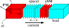
Slonczewski slon proposed a new method of switching the magnetization direction of a thin film by means of a spin-polarized current. The current is spin-polarized by passing through a thick polarizing magnet (PM), whose magnetization is assumed to be pinned, subsequently passing through a nonmagnetic metallic spacer layer of atomic planes and then through a thin magnetic switching layer (SM) into a nonmagnetic lead. We shall assume that the PM is semiinfinite and that its magnetization lies in the plane at an angle to the axis. The magnetization of the SM is assumed to be parallel to the axis. The spin polarized current (spin current) is partly or fully absorbed by the SM and the corresponding torque exerted on the SM can either switch its magnetization completely or lead to steady-state precession of the magnetizationexp1 ; exp2 . The current induced precession of magnetization results in microwave generation. Both effects have great potential for applications but the current density required for magnetization switching in a conventional junction, shown schematically in Fig.1a, is at present too large for commercial applications.
It is easy to see that there is an upper limit on what can be achieved with conventional switching junctions. The maximum spin current is obtained when all carriers are 100% spin polarized, and typical epitaxial junctions are already quite close to this theoretical limit. One way to reduce the current flowing through the switching magnet is to use a three-terminal deviceBrataas . However, a strong charge current still needs to be passed between the electrodes not involved in switching. The quest for a system in which no strong charge current flows anywhere in the system thus continues.
 |
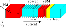 |
We propose that a very large reduction of the switching current can be achieved with a modified two-terminal junction shown in Fig1.b. The fundamental difference here is that a thin insulating layer is inserted between the switching magnet and the right lead. The charge current in such a junction is strongly reduced since it has to pass through a tunneling barrier. However, we shall show that one of the components of the spin current in the nonmagnetic spacer layer is only weakly affected by the barrier and remains large even when the barrier is thick. One can, therefore, generate a large spin-transfer torque with a very weak charge current. To calculate it, we shall use a rigorous theory of the spin currentedwards05 based on the Keldysh nonequilibrium formalism Keldysh applied to a single-orbital tight-binding model with nearest neighbor hopping and atoms on a simple cubic lattice. Generalization to a fully realistic band structure is straightforward and is described in edwards05, .
The Keldysh formalism gives us a completely rigorous prescription of how to calculate the steady-state spin and charge current from the equilibrium retarded one-electron Green’s functions and at the left and right surfaces of a junction cleaved between the planes and . It follows from Ref.edwards05 that the total spin current between atomic planes , is the sum of the equilibrium (zero bias) term and nonequilibrium (transport) term
| (1) |
| (2) |
Here, , , and is the Fermi function with chemical potential and . The summation in Eqs.(1) and (2) is over the in-plane wave vector and is the Pauli matrix. The charge current is calculated by replacing with the unit matrix. Since we only consider in the spacer where it is conserved, we drop the subscript .
In zero bias only the equilibrium component of the spin current perpendicular to the plane determined by the PM and SM magnetizations ( plane) is nonzero. It gives the equilibrium interlayer exchange coupling edwards05 . It should be noted that all occupied electron states contribute to the equilibrium coupling which is why Eq.(1) involves the integral with respect to energy. However, the equilibrium term (1) makes no contribution to the spin current linear in the bias, i.e. to first order in . In the context of current-induced switching we can thus ignore this term and focus on the transport contribution given by Eq.(2). To the lowest order in the bias (linear response), the Fermi functions in Eq.(2) are expanded to first order in . Hence the energy integral is avoided, being equivalent to multiplying the integrand by and evaluating it at the common zero-bias chemical potential . This shows explicitly that only states at the Fermi surface contribute, i.e., the term (2) is the nonequilibrium transport contribution to the spin current.
It is now well known (see e.g. edwards05 ; butler ) that the transport spin current in the NM spacer of a conventional switching junction (Fig.1a) has both in-plane and out-of-plane components. It has been argued (see e.g. Ref.butler ) that linear in vanishes so that this term exhibits a quadratic dependence on the applied bias. This is only true for a completely symmetric junction but not true for asymmetric junctions as originally pointed out in edwards05 and later confirmed in tang . Since the junction we propose (see Fig. 1(b)) is inherently highly asymmetric, linear in is nonzero, and it is this term linear in the applied bias which determines the transport out-of-plane torque.
Since the magnetization of the PM is in the plane the existence of the in-plane spin current is obvious but the origin of the out-of-plane component is less clear. Electrons emerging from the PM magnet have spin polarized in the xz-plane and, therefore, can only arise in a FM/NM/FM junction as a result of reflections from FM/NM interfaces.
This observation has lead us to consider a modified junction shown in Fig.1b in which an insulating layer (INS) is inserted between the SM and the right hand lead. When a bias is applied across the junction, bias driven electrons at the Fermi level incident from the left are strongly reflected at the SM/INS interface. The incident and reflected electron waves interfere to form almost perfect standing waves. To a very good approximation, they are described by a real note wavefunction with components and . Since and , it is obvious that the corresponding vanishes identically for real . The same argument applies to the charge current. On the other hand, is nonzero for a standing wave. It follows that the charge current and are strongly suppressed by the insulating layer but we expect that remains large and can even be enhanced by the insulating ‘reflector’. We emphasize that, for this effect to occur, it is crucial that the ‘reflector’ is placed behind the switching magnet. This is essential because incident and reflected electrons must travel across the whole trilayer and feel spin-dependent potentials of both the PM and SM. We call the junction in Fig.1b a reflecting junction.
The total transport spin current can be again evaluated from Eq.(2) where the surface Green’s functions and now include the effect of electron reflections at the SM/INS interface. In Fig.2 we plot the spin currents and , and the charge current as a function of the insulating barrier thickness . The angle between the magnetization of the PM and SM layers is taken to be and the thickness of the SM is 5 atomic planes. We have used the following values of tight-binding on-site potentials measured in units of : -2.3 and -2.8 for the majority and minority spin in the PM and in the SM, -2.0 in the spacer and the lead, and -3.1 in the insulating barrier. The thickness of the spacer is atomic planes. Such a choice of parameters models a Co/Cu/Co junction with a good matching of Co majority band with the Cu bands. For comparison, we include in Fig.2 also the results for a conventional switching junction corresponding to the insulating barrier thickness =0.
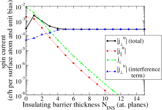
It can be seen that for a conventional junction (=0), the in-plane and out-of-plane spin currents are comparable in magnitude. However, the situation changes dramatically when an ‘reflector’ is inserted behind the switching magnet and the right lead. The in-plane component and the charge current decrease exponentially with the barrier thickness but the out-of-plane component saturates to a finite value which is quite close to the value of (and ) for a conventional junction. To understand these results, it is important to note that there are two different contributions to the out-of-plane spin current in the NM spacer. The first contribution is associated with the tunnelling charge current which carries with it an out-of-plane spin current component. This is the usual out-of-plane component of the spin current which is observed in conventional switching junctions. It is proportional to the charge current and thus decreases exponentially with the barrier thickness.
The second (interference) contribution to arises from interference between the incoming and reflected electron waves. It is shown in Fig.2 as triangles. It can be seen that it is the only contribution that remains finite for thick insulating layer. It arises because the bias driven electrons are almost totally reflected at the SM/INS interface and, therefore, almost perfect standing waves are formed in the NM spacer. The origin of the out-of-plane spin current can then be explained using the following simple model of a standing wave
| (3) |
where the coefficients and are real, is the perpendicular wave vector in the NM spacer, and is the position in the spacer. The phase shift between the majority- and minority-spin wave functions is a function of , where is the spacer thickness and is the lattice constant. The phase shift results in an out-of-plane component of the spin current
| (4) |
For a given electron state with a parallel wave vector , the interference contribution to the total out-of-plane spin current oscillates around zero as the spacer thickness increases. The oscillation period is given by . The total is obtained by summing over all states in the 2D Brillouin zone (see Eq.2). States with different have different oscillation periods and, therefore, interfere destructively. It follows Itoh that the oscillation amplitude of the integrated interference component of decreases with increasing spacer thickness. The total out-of-plane spin current is thus expected to oscillate with a decaying amplitude about a small constant background determined by the tunneling component. Since the magnitude of the spin current in the spacer of a reflecting junction decreases with the spacer thickness we need to establish that, for a realistic bias and realistic spacer thickness, the resultant torque on the switching magnet is at least as large as in a coventional junction and also that the transport torque is stronger than the equilibrium interlayer coupling torque . The torque exerted on the switching magnet is the difference between the spin currents in the spacer and right lead. To evaluate the torque, we note that the transport spin current in the right lead has only the tunneling component of which is negligible compared with the interference component of in the spacer. The equilibrium spin current in the lead is strictly zero. It follows that both torques and are given by the corresponding spin currents in the spacer. The fact that in a reflecting junction with a spacer thickness of the order of 10 atomic planes can be as large as the torque in a conventional junction is already evident from Fig.2. We, therefore, only need to compare the transport torque with the equilibrium coupling torque . Since the transport torque is proportional to the bias , it is necessary to choose for this comparison a value of small enough for the linear-response approximation adopted here to be valid. A value , where is the band width, satisfies this requirement since the voltage drop across the barrier is negligible compared with the barrier height ( in Fig.2). We note that, to the lowest order (linear) in , the equilibrium coupling torque is independent of the bias. Using , which corresponds to a bias for , we compare in Fig.3 the transport and equilibrium coupling torques assuming that the angle between the PM and SM magnetizations is . The tight binding parameters are the same as in Fig.2.
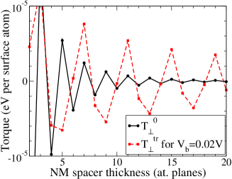
Both torques oscillate with decreasing amplitude as the thickness of the spacer increases. However, the amplitudes, periods, and decay rates of the equilibrium and transport torque oscillations are quite different, which clearly demonstrates their fundamentally different origins. We first note that, even for the very low bias of , the transport torque is much stronger than the coupling torque. There is, therefore, no problem in overcoming the static coupling term by the bias-dependent transport term. Moreover, since the two torques oscillate with different periods, one can always select a spacer thickness where the static coupling is close to zero and thus eliminate this term altogether.
We now briefly discuss the oscillation periods and decay rates of and . It is well known coupling that the static torque decays as , where is the thickness of the spacer. The corresponding oscillation period is given by the spacer Fermi surface (FS) spanning vector coupling (2 atomic planes in our case). The periods obtained from the extrema of the spacer FS are the only periods that can occur for the equilibrium coupling torque coupling . However, the transport torque can also oscillate with additional periods arising from sharp cutoffs of the sum over in Eq.(2) (the cutoff periods are removed from the equilibrium coupling term by the energy integral in Eq.(1) Itoh ). The origin of the cutoff periods was discussed by Mathon et al. Itoh in the case of charge current oscillations, and the same arguments apply here. Finally, the decay of the transport torque oscillations with spacer thickness should be slower than the decay rate of the static coupling. This is because the additional destructives interference that arises from the energy integration in the static coupling term (Eq.1) is not present in the transport term (eq.2). In the case shown in Fig.3, the oscillation period of the transport torque is clearly dominated by a cutoff period which is atomic planes for the potentials we have chosen. The decay rate of is slower than that of the coupling torque (see e.g. Itoh ).
Finally, we point out that although our results are for a switching (SM) thickness of 5 atomic planes, qualitatively similar results are obtained for other SM thicknesses. Varying the thickness of the SM has only a small effect on the transport torque , i.e. it oscillates with a small amplitude around a finite constant background as the SM thickness increase. This is because most of the interference responsible for occurs in the spacer.
The reflecting junction we propose offers huge potential advantages over the conventional junction. Firstly, a strong out-of-plane spin-transfer torque can be generated by an applied bias without the accompanying charge current. The bias strength is not limited to the linear-response regime considered here. Generalization to a strong bias simply requires energy integration in Eq.(2) between and . The applied bias is then limited only by the barrier height. The second advantage of the reflecting junction is that the magnitude and sign of the ratio can be tuned by the height/width of the reflecting barrier and by the spacer thickness. This is important since the ratio controls switching scenarios E+M . For example, with the appropriate sign of this ratio, microwave generation can be achieved without an applied magnetic field E+Mreview .
A bias controled switching was proposed earlier in suzuki . However, the physical mechanism behind this idea is completely different. It is based on a bias induced modification of the equilibrium interlayer coupling and ignores completely the transport term considered here. However, as already discussed, the modification of the equilibrium coupling by a bias is a higher order effect which vanishes to the first order in the bias.
Since the out-of-plane torque arises from interference between incident and reflected electron waves one needs good interfaces to observe and exploit it. However, the quality of the interfaces need not be any better than that required for observation of the usual interlayer exchange coupling, which is also an interference effect. In addition, the quality of the SM/INS interface may also be important. However since the main role of the insulator is to suppress the charge current, the quality of this interface may not be so crucial. Furthermore, it is known from experiments on tunneling junctions with MgO barrier that the Fe/MgO interface can be grown almost perfectly epitaxial, and we suggest that this combination would be an ideal choice for the reflecting junction. Finally, we would like to mention that an insulating barrier could be replaced by a doped semiconductor layer such as InAs which forms an ohmic contact with SM (e.g. Fe). This might allow a finer tuning of the ratio since the spin current that can flow through the junction could be controlled by doping (size of the semiconductor FS).
Acknowledgements.
We are grateful to the UK Engineering and Physical Sciences Research Council for financial support.References
- (1) J. C. Slonczewski, J. Magn. Magn. Mater. 159, L1 (1996); 195, L261 (1999).
- (2) J.A. Katine, F.J. Albert, R.A. Buhrman, E.B. Myers and D.C. Ralph, Phys. Rev. Lett. 84, 3149 (2000).
- (3) S.I. Kiselev, J.C. Sankey, I.N. Krivorotov, N.C. Emley, R.J. Schoelkopf and R.A. Buhrman, D.C. Ralph, Nature 425, 380 (2003).
- (4) K. Xia, P. J. Kelly, G. E. W. Bauer, A. Brataas, and I. Turek, Phys. Rev. B 65, 220401(R) (2002).
- (5) D. M. Edwards, F. Federici, J. Mathon, and A. Umerski, Phys. Rev. B 71, 054407 (2005).
- (6) L. V. Keldysh, Sov. Phys. JETP 20, 1018 (1965).
- (7) I. Theodonis, N. Kioussis, A. Kalitsov, M. Chshiev and W. H. Butler, Phys. Rev. Lett. 97, 237205 (2006).
- (8) Y.-H. Tang, N. Kioussis, A. Kalitsov, W. H. Butler, and R. Car, Phys. Rev. B 81, 054437, (2010).
- (9) Note that is never strictly real. It would be real only for an infinitely high insulating barrier, in which case the junction would cease to be a nonequilibrium system.
- (10) D. M. Edwards, J. Mathon, R. B. Muniz and M. S. Phan, Phys. Rev. Lett. 67, 493 (1991).
- (11) J. Mathon, Murielle Villeret, and H. Itoh, Phys. Rev. B 52, R6983 (1995).
- (12) D.M. Edwards and J. Mathon, Current induced switching of magnetization, in Nanomagnetism, ed. by D.L. Mills and J.A.C. Bland, Elsevier (2006), p. 273.
- (13) D.M. Edwards and J. Mathon, Theory of spin current in magnetic, J. Phys.: Condens. Matter 19, 165210 (2007).
- (14) C.-Y. Youa and Y. Suzuki, J. Magn. Magn. Mater. 293 (2005).