Transport Gap in Suspended Bilayer Graphene at Zero Magnetic Field
Abstract
We report a change of three orders of magnitudes in the resistance of a suspended bilayer graphene flake which varies from a few ks in the high carrier density regime to several Ms around the charge neutrality point (CNP). The corresponding transport gap is 8 meV at 0.3 K. The sequence of appearing quantum Hall plateaus at filling factor followed by suggests that the observed gap is caused by the symmetry breaking of the lowest Landau level. Investigation of the gap in a tilted magnetic field indicates that the resistance at the CNP shows a weak linear decrease for increasing total magnetic field. Those observations are in agreement with a spontaneous valley splitting at zero magnetic field followed by splitting of the spins originating from different valleys with increasing magnetic field. Both, the transport gap and field response point toward spin polarized layer antiferromagnetic state as a ground state in the bilayer graphene sample. The observed non-trivial dependence of the gap value on the normal component of suggests possible exchange mechanisms in the system.
pacs:
73.22.Pr, 72.80.Vp, 73.43.Qt, 85.30.TvI Introduction
Followed by the isolation of single layer graphene, the study of bilayer graphene (BLG) became a separate direction of research in the community of two dimensional materials. Charge carriers in bilayer graphene have a parabolic dispersion with an effective mass of about 0.054me,McCann (2006); McCann and Fal’ko (2006) but also possess a chirality. The latter manifests itself in an unconventional quantum Hall effectNovoselov et al. (2006) with the lowest Landau level (LLL) being eight fold degenerate. Compared to single layer, bilayer graphene has next, to spin and valleys degrees of freedom, an additional orbital degree of freedom, where Landau levels with numbers n = 0 and 1 (each four fold degenerate) have the same energy.Novoselov et al. (2006); McCann and Fal’ko (2006) Recent advances in obtaining suspended bilayer graphene devices with charge carrier mobility exceeding gave access to the investigation of many-body phenomena in clean bilayer graphene at low charge carrier concentration ().Feldman et al. (2009); Weitz et al. (2010); Martin et al. ; Velasco et al. (2012); van Elferen et al. (2012); Freitag et al. (2012); Mayorov et al. (2011); Bao et al. (2012)
Due to the non vanishing density of states at the charge neutrality point (CNP), bilayer graphene is predicted to have a variety of ground states triggered by electron-electron interaction. There are two competing theories describing the ground state of BLG: a transition (i) to a gapped layer polarized state (excitonic instability)Nandkishore and Levitov (2010a, b); Min et al. (2008); Zhang et al. (2010); Jung et al. (2011); Zhang et al. (2011) or (ii) to a gapless nematic phase.Vafek and Yang (2010); Lemonik et al. (2010); Tőke and Fal’ko
Excitonic instability is a layer polarization in which the charge density contribution from each valley and spin spontaneously shifts to one of the two graphene layers.Jung et al. (2011); Zhang et al. (2011) This redistribution is caused by an arbitrarily weak interaction between charge from conduction and valence band states.Nandkishore and Levitov (2010a, b) Since each bilayer flavor (spin or valley) can polarize towards either of the two layers, there are 16 possible states,Jung et al. (2011); Zhang et al. (2011) which can be classified by the total polarization as being ferromagnetic (all degrees of freedom choose the same layer), ferrimagnetic (three of the four valley-spin flavors choose the same layer), or antiferromagnetic (with no overall polarization). To make it clear, the therm should be associated to flavors (not only spin) orientation in between two layers. These states are considered as analogous to the biased bilayerCastro et al. (2007) in the sense that the charge transfer can be attributed to the (wave vector dependent) exchange potential difference between low-energy sites on the opposite layers.Jung et al. (2011) The total energy of the system is lowered by the gain in the exchange interaction via breaking of the inversion symmetry, i.e. introducing a gapped state. Antiferromagnetic polarization is electrostatically favorable due to the absence of a net charge on both layers, however, the actual ground state is theoretically undefined.Nandkishore and Levitov (2010a); Zhang et al. (2011); Jung et al. (2011) Recent experiments have suggested the evidence of the possible existence of two of the antiferromagnetic states - the anomalous quantum Hall state (AQH)Weitz et al. (2010); Martin et al. and spin polarized layer antiferromagnetic state (LAF)Velasco et al. (2012). To avoid possible confusion we note that in earlier literatureJung et al. (2011) the LAF state is also called quantum valley Hall state. The AQH has electrons being polarized in the same layer for both spins and in opposite layers for opposite valleys.Zhang et al. (2011); Jung et al. (2011) This state has spontaneously broken time reversal symmetry and therefore possess a substantial orbital magnetization exhibiting quantized Hall effect (at zero magnetic field), while its spin density is everywhere zero.Zhang et al. (2011) Due to its magnetization the AQH can be favored over other ground states in the perpendicular magnetic field. The LAF state has opposite spin-polarization for opposite layers. In contrast to AQH, the LAF state does not have topologically protected edge states, which brings its minimum conductance to zero. For both states the theoretical estimations of the gap give the value of 1.5-30 meV.Nandkishore and Levitov (2010b); Jung et al. (2011) However, the inter-valley exchange weakly favors the LAF state.Jung et al. (2011); Zhang and MacDonald One of the ways to determine the character of the bilayer ground state experimentally is to investigate the response of the gap value to the magnetic field (which couples to spin) and electrical field (which couples to layer pseudospin).Zhang and MacDonald When Zeeman coupling is included, the QAH state quasiparticles simply spin-split, leaving the ground state unchanged but the charge gap reduced. It was calculated that for a 4 meV spontaneous gap at zero-field, a field of = 35 T drives the gap to zero. On the other hand, the gap of LAF is weakly field dependent.
The second possible description for the ground state of BLG is based on a nematic phase caused by the renormalization of the low energy spectrum.Vafek and Yang (2010); Lemonik et al. (2010) Detailed tight-binding model studies showed that including next-neighbor interlayer coupling changes the band structure in bilayer producing a Lifshitz transition in which the isoenergetic line about each valley is broken into four pockets with linear dispersion.McCann and Fal’ko (2006); McCann et al. (2007) At the energies higher then 1 meV the four pockets merge into one pocket with the usual quadratic dispersion. Moreover, electron-electron interactions might result in the further energy spectrum transformation, where the number of low energy cones can be reduced to two near each of the two points.Vafek and Yang (2010); Lemonik et al. (2010) In this case the minimum conductance of the bilayer graphene is supposed to be increased comparing to bilayer with parabolic dispersion (). This scenario was also supported by the experimental result on the suspended bilayer graphene in which strong spectrum reconstructions and electron topological transitions were observed.Mayorov et al. (2011)
In this paper we present electric transport properties of suspended bilayer graphene by studying its behavior in tilted magnetic fields. At = 0 T we observe the spontaneous opening of a gap by changing charge carrier density from the metallic regime () to the CNP. At a temperature of 1 K we measure a resistance increase from 5 k up to 14 M. The observation indicates the gapped ground state of the studied bilayer graphene with a value of 6.8 meV. Measurements in tilted magnetic field showed that the resistance at the CNP decreases with an increasing of magnetic field. Based on this we propose a possible scenario of the symmetry breaking in this bilayer graphene sample: Spontaneous valley splitting at zero magnetic field followed by the splitting of the spins originating from different valleys with increasing of . Both, the gap value and its weak linear decrease with , supports LAF as the ground state of the studied sample.
II Experimental details
Suspended bilayer graphene devices were prepared using an acid free technique.Tombros et al. (2011a, b) We deposited highly ordered pyrolytic graphite on Si/SiO2 wafer (500 nm thick) which is covered with an organic resist LOR (1.15 m). A standard lithography procedure is performed in order to contact bilayer graphene flakes (determined by their contrast in optical microscope) with 80 nm of Ti/Au contacts. A second electron beam lithography step is used to expose trenches over which graphene membrane becomes suspended. To achieve high quality devices we use current annealing technique by sending a DC current through the membrane (up to 1.1 mA) at the temperature of 4.2 K. While ramping up the DC current, simultaneously, we keep track of the sample resistance. Once the resistance reaches values in the order of 10 ks we stop annealing and check the gate voltage dependence. We repeat this procedure till the appearance of a sharp resistance maximum at the CNP located close to zero . More details on the current annealing procedure can be found in Tombros Tombros et al. (2011b) The studied device was 2 m long and 2.3 m wide. All measurements were performed in four-probe geometry (with contacts across the full width of graphene) at the temperatures from 4.2 K down to 300 mK. The four-probe method allows to eliminate contact resistances. As discussed below the resistance measurements consist of a superposition of longitudinal magnetoresistance () and Hall-resistance (). The carrier density in graphene is varied by applying a DC voltage () between the back gate electrode () and the graphene flake. Based on serial capacitors model a unit capacitance of the system is 7.2 aF, which relates gate voltage with density as where is a leverage factor of . The typical current we use is around 1 nA. See Appendix.
III Temperature dependence and Quantum transport
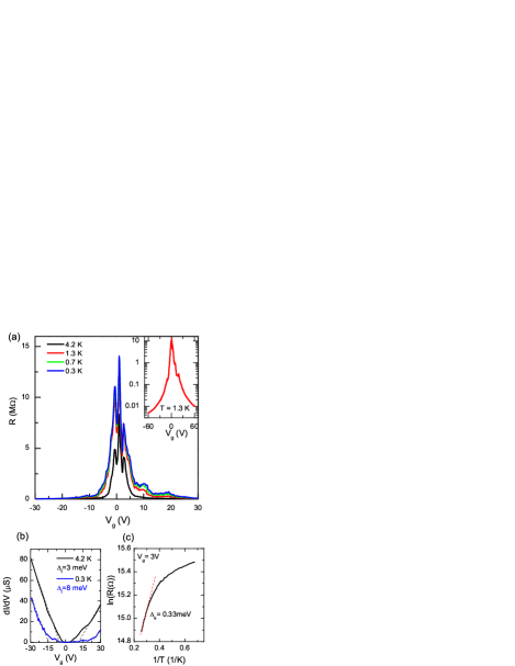
Our pristine samples are strongly p-doped with the CNP situated beyond 60 V and a metallic resistance of a few hundreds of s over the entire voltage range. Therefore we perform current annealing technique in order to obtain high quality devices. In contrast to previous samples, in which each next step of current annealing tend to cause sharper change in the resistance values within the scanned region of , the discussed bilayer sample already shows after the first current annealing step a high resistive region around the CNP (not shown). The next annealing step (1.1 mA) moves the charge neutrality point down to = 3 V. However, surprisingly the resistance around CNP becomes 14 M and reduces down to 5 k in the metallic regime at (Fig. 1a, Inset). This fact points toward opening of a gap. The temperature dependence of the membrane from 4.2 K to 300 mK is shown in Fig. 1a. There is an essential change of about 6 M in the maximum resistance () from 4.2 K down to 1.3 K, however further lowering of temperature does not change much. From an Arrhenius plot of the resistance at CNP (Fig. 1c) we can extract a thermal excitation gap of 0.33 meV.Xia et al. (2010) The saturation of resistance at lower T can be explained by a variable range hopping with different temperature dependence. We would like to point out that our excitation current value of 1 nA gave a voltage drop of mV at the CNP, which is much higher than energy at measured temperatures (0.3 meV). Therefore one has to be careful in comparing transport and thermal excitation gaps.
There might be a couple of scenarios for the observed gap formation in the gate voltage dependence: (i) A lateral confinement in membrane, where energy levels are
| (1) |
= 2.3 m - width of the flake, is integer value. However, first two levels have energies of = 1.3 eV and = 5.3 eV, which is much lower than at measured temperatures. (ii) True gap formation with zero density of states within the gap and available states at the conduction and valence bands. (iii) Transport gap, accompanied by the observation of the reproducible conductance oscillations in the region of suppressed conductance. In such regime transport is limited by the quantum confinement effect along the width (mainly originating from the impurities).Molitor et al. (2010) (iv) More complicated case, when the gap value depends on the charge carrier density, the energy of the levels changes while being filled with carriers. This situation might happen when the gap is induced by charge redistribution in between layers, which would be influenced by the applied back gate voltage. At the moment, we can not determine the exact gap type, therefore, further analysis is performed assuming a transport gap scenario, but keeping in mind that this gap value can depend on the density.
In an analogy to graphene nanoribbon studiesMolitor et al. (2010); Stampfer et al. (2009) we extract the transport gap from the gate dependence of the sample conductance as shown in Fig. 1b). From a linear approximation of conductance one gets a region of , where sample shows insulating behavior. This region relates to the wave vector as . Taking into account the quadratic dispersion of bilayer graphene, the corresponding energy scale can be calculated as
| (2) |
From conductance graphs at different we find at 4.2 and at 0.3 . The values of the transport gap are comparable to the energy gap (extracted in bias direction) values of single layer graphene nanoribbons of 50-85 nm wide,Molitor et al. (2010); Stampfer et al. (2009) where in contrast to our case the gap is created by lateral confinement. The resistance value of 5 k in metallic regime, similar to regular graphene devices, serves as an additional justification of excluding a lateral confinement as a cause of the observed transport gap. We can calculate the mobility of the charge carriers using a standard formula , where is a square resistance of the sample and is elementary charge. The mobility value at corresponds to the value of high quality bilayer graphene devices. Due to the symmetry of resistance change around CNP (Fig. 1b) and the fact that CNP itself is situated around zero gate voltage ( = 1.2 V), that corresponds to the density of at 0 V, we can also exclude the low quality ”p-doped” regions close by the contacts (which can form after current annealing) as the cause of the reported gap. In the meantime, we can not exclude a charge inhomogeneity in the sample bulk which might lead to the observed order of magnitude deference between electrical and transport gaps, in analogy to nanoribbon case.
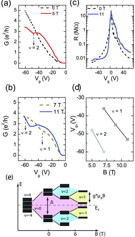
Given the fact that the resistance values reach Ms at the CNP, it is already hard to establish quantum Hall plateaus in our suspended bilayer device. However, we have achieved to observe quantum Hall transport shown in Fig. 2a,b). First quantum Hall plateau appears at 5 T on electron side (red curve), which we attribute to the filling factor . This plateau is followed by the appearance of at 7 T (Fig. 2b). The conductance values of the observed plateaus deviate from the expected ones of and , since they are affected by charge inhomogeneity. Therefore, we determine the exact values of the corresponding plateaus by the scaling of their positions in density () with magnetic field (Fig. 2d). As expected from the scaling is linear with the leverage factor of for and . In order to use the same for both filling factor sets (see Fig. 2d) the slopes of versus ; and values respectively, have to be twice as different. Therefore, we have to point out that the linear scaling will hold as well for a leverage factor of in case we assume and as an observed sequence of plateaus. From previous studiesVera-Marun et al. we know that capacitance probed by the QHE in graphene devices (especially in suspended samples) can be higher than the geometrical value, due to the deviation from the plane capacitor model. However, we attribute the observed plateaus to the filling factors 2 and 1. As we noticed before,Tombros et al. (2011a); van Elferen et al. (2012) most of the time the current annealing procedure leads to the formation of high quality annealed regions connected in series with low mobility p-doped regions close to the contacts. Therefore higher values of the conductance plateaus can be explained by a ”p-doped” slope, which increases with magnetic field . This can be also the reason of the absence of resistance quantization in the electron-side (Fig. 2c). Assuming 1 for the formation of QHE plateaus,Bolotin et al. (2008) our observation implies a lower bound for the mobility of 2,000 .
To summarize our QH transport results: At this point we have shown that a zero-field gap opens at the CNP in the studied graphene bilayer. This observation points out on a possible symmetry breaking of the ground state in bilayer graphene. The application of does not restore the broken symmetry and brings the systems in to the QH regime. In Fig. 2e) we show the hierarchy of the splitting of the 8-fold degenerate lowest Landau level in applied .Zhao et al. (2010) The development of the level structure with will be specified and discussed in section 4. In the meanwhile, if we assume that at = 0 T one of the degeneracies is already lifted, then, with increasing field, one can expect quantization at the filling factors and followed by and . However, if the initial symmetry breaking is strong enough and the scanned window in energy is limited (), then one can expect quantization at followed by . This described hierarchy of levels splitting and sequence of plateaus will be observed independent on either valleys or spin splitting first.
IV Resistance at the CNP in tilted magnetic field
In order to clarify the nature of the gapped ground state of bilayer graphene and its evolution in magnetic field we perform a tilted magnetic field experiment. In tilted experiments the total magnetic field () can be separated from its normal (to the plane of the sample) component: , where is an angle between these two vectors (Fig. 3c). This procedure allows us to distinguish between the orbital effect (QHE) and pure Zeeman energy, which has to scale with value.Zhao et al. (2010); Zhang and MacDonald ; Kurganova et al. (2011)
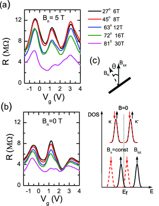
All measurements presented below were performed at a temperature of 1.3 K. The application of the magnetic field perpendicular to the sample plane leads to an increase in the resistance at the CNP, as it is expected for a QH transport in the case of broken symmetry states. To distinguish between normal component and total we perform a series of experiments with keeping fixed and gradually increasing . As an example, in Fig. 3a) we show a change in at = 5 T and increasing from 6 T up to 30 T for different angles . The actual maximum of the resistance consists of three peaks: highly resistive in the middle ( = 1.2 V) and two side peaks at the gate voltage at -0.5 and 3 V. The total magnetic field causes decrease in the resistance and the middle peak starts splitting into two peaks (or developing minimum in resistance at the CNP) when 6 T for studied values of . We observe exactly the same behavior in the experiment when = 0 and applied field is in parallel to the graphene membrane: maximum of the resistance goes down and develops a local minimum at the CNP (Fig. 3b). We attribute this change with an increase of the total magnetic field. That fact that resistance changes with indicates that observed effect is not a simple quantum localization due to inhomogeneity in the sample.

All three maxima around the CNP decrease in their resistance in applied parallel . However, only the middle maximum at = 1.2 V shows clear scaling with the total magnetic field () at different tilted angles (Fig. 4a). As one can see in the case of (, black curve in Fig. 4a) the resistance keeps on increasing up to around 14 T; further increase in magnetic field brings to lower values (Fig. 4a). Once the non zero angle is introduced the common trend for is a decrease.
We suggest that the behavior of the middle peak is caused by the many-body effect and can be explained by the Zeeman splitting closing the spontaneous gap. The hierarchy of energy levels is depicted in Fig. 2e). Once value is high enough the LLL is split in to 4 levels, each two-fold degenerate. If we assume that the latter degeneracy is spin, then after the appearance of plateau associated with filling factor we expect the value of the ground state gap to be lowered by spin splitting coupled to . Here we would like to emphasize, that we do observe appearance of and minimum of resistance at the CNP in similar magnetic field T. In a simplified way we describe resistance value at the CNP point as
| (3) |
where is an effective -factor including exchange electron interaction and a Landau level broadening.Nicholas et al. (1988); Kurganova et al. (2011); van Elferen et al. (2012) The change in ln() versus at fixed values is shown in Fig. 4b). This dependence can be the best described as linear. The slope and y-intercept of the linear fit of Fig. 4b) give the values of and . Surprisingly, these both contributions scale with component. In Fig. 4c) we show values versus . Despite the fact that the scaling seems like linear, plotting the slope as a function of does seem like fitting as well (not shown). value increases with from 1.4 meV at = 1 T up to 1.7 meV at = 25 T (not shown). This is of the same order as the measured transport gap (which can overestimate a real energy gap) and also corresponds to the theoretically predicted gap of 1.5-30 meV for the excitonic instability.Nandkishore and Levitov (2010b); Jung et al. (2011); Zhang and MacDonald
In summary, tilted magnetic field experiments show that the resistance at the CNP of studied gapped bilayer graphene decreases linearly with the total magnetic field component. This points to a many-body effect and weak reduction of the gap in applied magnetic field. The developed minimum in the resistivity in Fig. 3 can be explained by the overlapping of spin-up and spin-down levels from the adjacent Landau levels due to Zeeman splitting in applied .Nicholas et al. (1988) However, from our experiments the estimated 0.2, which is very low for spin splitting. In addition, although the resistance decreases in parallel field, the value does not change an order of magnitude. This behavior in is consistent with the layer antiferromagnetic state as a ground state of studied bilayer sample.Zhang and MacDonald Since in this state the top and bottom layers host spins with opposite orientations, their interaction with applied can not be described as a simple Zeeman splitting. Next to it, our results also open an additional question: What is the role of exchange energy and level broadening in LAF state? Naively, scaling of with can be understood from their dependence on level broadening . The value scales with , meaning the bigger the smaller is needed to observe level’s overlapping. In reality the situation can be much more complicated including possible exchange mechanisms we do not understand yet. This is also supported by the fact that the ground state gap depends on as well.
Based on these results we suggest a possible scenario of symmetry breaking in high quality bilayer graphene (Fig. 2e and Fig. 3c). First splitting is caused by valleys, which results in the observed transport gap. An application of magnetic field induces spin splitting of both and levels. When is high enough then the energy of spin-up level from will start approaching the spin-down level from . The overlapping of the levels will cause a decrease in the resistance at the charge neutrality point. Since we do observe transport gap in our sample, we exclude nematic phase transition. In addition to this, the response of the sample in tilted fits to the LAF state. The cause of the valley splitting can be a combination of two effects: electron-electron interaction (which determines the field behavior of the middle resistance maximum ) and a contamination of the sample surface with charged impurities which break inversion symmetry (via introduction of electrical field).Castro et al. (2007)
V Conclusions
We report a transport gap of 3 meV in suspended bilayer graphene at 4.2 K, which increases with decreasing of temperature. The sequence of appearance of the QHE plateaus at the filling factor followed by supports a suggestion that the observed gap caused by the symmetry breaking. Measurements in the tilted magnetic field indicates that the resistance at the CNP shows weak linear decrease with the total magnetic field component. Based on this we propose a possible scenario of the symmetry breaking in the investigated bilayer graphene: Spontaneous valley splitting at zero magnetic filed followed by the splitting of the spins originating from different valleys with increasing of . The gap value and weak response of the sample to applied magnetic field corresponds to the predicted spin polarized layer antiferromagnetic state as a ground state of the investigated sample. The observed non-trivial dependence of the gap value from the normal component of suggests possible exchange mechanisms in the system.
Acknowledgements.
We would like to thank B. Wolfs, M. de Roosz and J.G. Holstein for technical assistance. We also thank M.H.D. Guimarães for useful discussions; and I.J. Vera-Marun for creating a soft-wear program for current annealing. This work is supported by NWO (via TopTalent grant), FOM, NanoNed and the Zernike Institute for Advanced Materials.VI Appendix
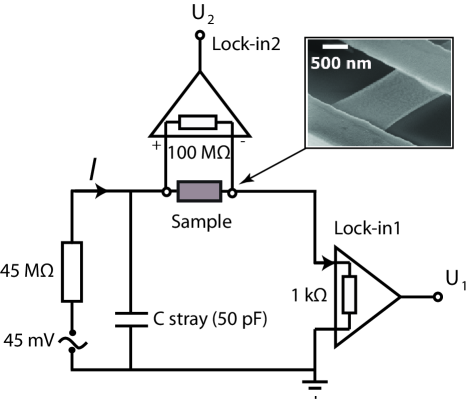
In order to minimize self-heating in graphene at the high resistive CNP we used the following scheme (Fig. 5). An AC source maintained a fixed voltage amplitude of 45 mV (1.87 Hz frequency) across the sample in series with 45 M resistor. The current through the sample is monitored by the lock-in1, whose output is proportional to the current flowing in the circuit (). Simultaneously, the four probe voltage across the sample () is phase detected by another lock-in2 connected through the preamplifier having an input resistance up to 100 M. Then the resistance of the sample is determined by . The power dissipating in the sample is . Therefore, assuming that maximum is already reached ( mV), with increasing of the dissipation in the sample will be decreasing.
References
- McCann (2006) E. McCann, Phys. Rev. B 74, 161403 (2006).
- McCann and Fal’ko (2006) E. McCann and V. I. Fal’ko, Phys. Rev. Lett. 96, 086805 (2006).
- Novoselov et al. (2006) K. S. Novoselov, E. McCann, S. V. Morozov, V. I. Fal’ko, M. I. Katsnelson, U. Zeitler, D. Jiang, F. Schedin, and A. K. Geim, Nature Phys. 2, 177 (2006).
- Feldman et al. (2009) B. E. Feldman, J. Martin, and A. Yacoby, Nature Phys. 5, 889 (2009).
- Weitz et al. (2010) R. T. Weitz, M. T. Allen, B. E. Feldman, J. Martin, and A. Yacoby, Science 330, 812 (2010).
- (6) J. Martin, B. E. Feldman, R. T. Weitz, M. T. Allen, and A. Yacoby, Phys. Rev. Lett. 105, 256806.
- Velasco et al. (2012) J. J. Velasco, L. Jing, W. Bao, Y. Lee, P. Kratz, V. Aji, M. Bockrath, C. Lau, C. Varma, R. Stillwell, D. Smirnov, F. Zhang, J. Jung, and A. MacDonald, Nature Nano. 7, 156 (2012).
- van Elferen et al. (2012) H. J. van Elferen, A. Veligura, E. V. Kurganova, U. Zeitler, J. C. Maan, N. Tombros, I. J. Vera-Marun, and B. J. van Wees, Phys. Rev. B 85, 115408 (2012).
- Freitag et al. (2012) F. Freitag, J. Trbovic, M. Weiss, and C. Schönenberger, Phys. Rev. Lett. 108, 076602 (2012).
- Mayorov et al. (2011) A. S. Mayorov, D. C. Elias, M. Mucha-Kruczynski, R. V. Gorbachev, T. Tudorovskiy, A. Zhukov, S. V. Morozov, M. I. Katsnelson, V. I. Fal’ko, A. K. Geim, and K. S. Novoselov, Sience 33, 860 (2011).
- Bao et al. (2012) W. Bao, J. Velasco, F. Zhang, L. Jing, B. Standley, D. Smirnov, M. Bockrath, A. MacDonald, and C. N. Lau, preprint , arXiv:1202.3212v1 (2012).
- Nandkishore and Levitov (2010a) R. Nandkishore and L. Levitov, Phys. Rev. Lett. 104, 156803 (2010a).
- Nandkishore and Levitov (2010b) R. Nandkishore and L. Levitov, Phys. Rev. B 82, 115431 (2010b).
- Min et al. (2008) H. Min, G. Borghi, M. Polini, and A. H. MacDonald, Phys. Rev. B 77, 041407 (2008).
- Zhang et al. (2010) F. Zhang, H. Min, M. Polini, and A. H. MacDonald, Phys. Rev. B 81, 041402 (2010).
- Jung et al. (2011) J. Jung, F. Zhang, and A. H. MacDonald, Phys. Rev. B 83, 115408 (2011).
- Zhang et al. (2011) F. Zhang, J. Jung, G. A. Fiete, Q. Niu, and A. H. MacDonald, Phys. Rev. Lett. 106, 156801 (2011).
- Vafek and Yang (2010) O. Vafek and K. Yang, Phys. Rev. B 81, 041401 (2010).
- Lemonik et al. (2010) Y. Lemonik, I. L. Aleiner, C. Toke, and V. I. Fal’ko, Phys. Rev. B 82, 201408 (2010).
- (20) C. Tőke and V. I. Fal’ko, arXiv:0903.2435v1 .
- Castro et al. (2007) E. V. Castro, K. S. Novoselov, S. V. Morozov, N. M. R. Peres, J. M. B. L. dos Santos, J. Nilsson, F. Guinea, A. K. Geim, and A. H. Castro Neto, Phys. Rev. Lett. 99, 216802 (2007).
- (22) F. Zhang and A. H. MacDonald, arXiv:1107.4727v1 .
- McCann et al. (2007) E. McCann, D. S. Abergel, and V. I. Fal’ko, Solid State Commun. 143, 110 (2007).
- Tombros et al. (2011a) N. Tombros, A. Veligura, J. Junesch, J. J. van den Berg, P. J. Zomer, M. Wojtaszek, I. J. Vera-Marun, H. T. Jonkman, and B. J. van Wees, Jour. Appl. Phys. 109, 093702 (2011a).
- Tombros et al. (2011b) N. Tombros, A. Veligura, J. Junesch, M. H. D. Guimaraes, I. J. Vera-Marun, H. T. Jonkman, and B. J. van Wees, Nature Phys. 7, 697 (2011b).
- Xia et al. (2010) F. Xia, D. B. Farmer, Y.-m. Lin, and P. Avouris, NanoLetters 10, 715 (2010).
- Molitor et al. (2010) F. Molitor, C. Stampfer, J. Güttinger, A. Jacobsen, T. Ihn, and K. Ensslin, Semicond. Sci. Technol. 25, 034002 (2010).
- Stampfer et al. (2009) C. Stampfer, J. Güttinger, S. Hellmüller, F. Molitor, K. Ensslin, and T. Ihn, Phys. Rev. Lett. 102, 056403 (2009).
- (29) I. J. Vera-Marun, P. Zomer, A. Veligura, M. H. D. Guimaraes, L. Visser, N. Tombros, H. J. van Elferen, U. Zeitler, and B. J. van Wees, arXiv:1112.5462v1 .
- Bolotin et al. (2008) K. I. Bolotin, K. J. Sikes, Z. Jiang, M. Klima, G. Fudenberg, J. Hone, P. Kim, and H. L. Stormer, Solid State Commun. 146, 351 (2008).
- Zhao et al. (2010) Y. Zhao, P. Cadden-Zimansky, Z. Jiang, and P. Kim, Phys. Rev. Lett. 104, 066801 (2010).
- Kurganova et al. (2011) E. V. Kurganova, H. J. van Elferen, A. McCollam, L. A. Ponomarenko, K. S. Novoselov, A. Veligura, B. J. van Wees, J. C. Maan, and U. Zeitler, Phys. Rev. B 84, 121407 (2011).
- Nicholas et al. (1988) R. J. Nicholas, R. J. Haug, K. v. Klitzing, and G. Weimann, Phys. Rev. B 37, 1294 (1988).