All-electrical injection and detection of a spin polarized current using 1D conductors
Abstract
All-electrical control of spin transport in nanostructures has been the central interest and challenge of spin physics and spintronics. Here we demonstrate on-chip spin polarizing/filtering actions by driving the gate-defined one dimensional (1D) conductor, one of the simplest geometries for integrated quantum devices, away from the conventional Ohmic regime. Direct measurement of the spin polarization of the emitted current was performed when the momentum degeneracy was lifted, wherein both the 1D polarizer for spin injection and the analyzer for spin detection were demonstrated. The results showed that a configuration of gates and applied voltages can give rise to a tunable spin polarization, which has implications for the development of spintronic devices and future quantum information processing.
There is considerable interest in being able to control spin dynamics, particularly in mesoscopic and nanoscale semiconductor deviceszutic_rmp04 ; fert_rmp08 as this could lead to the development of a range of electronic functions not presently available. In order to develop successfully such concepts it is necessary to controllably generate, manipulate, and detect spin currents by electrical means and so minimize, or eliminate, the use of ferromagnetic contacts or external magnetic fields. Most research towards the implementation of this electrical approach has focussed on using the spin-orbit interaction to induce spin polarized transport, as reported in various nanostructureskato_science04 ; konig_science07 ; hsieh_nature08 ; frolov_nature09 including one-dimensional (1D) conductorsdebray_naturenano09 ; qua_naturephys10 . However, it is essential to develop a more general approach in which materials with a strong intrinsic spin-orbit coupling are no longer necessary, and consequently a longer spin dephasing (relaxation) time will be obtained of crucial importance for quantum information processing.
In theory, it is possible to produce transition from anti-ferromagnetic to ferromagnetic behaviour by controlling the exchange interaction, although this can be difficult to achieve in practice. If such a mechanism could be successfully utilized for on-chip spin injection, the problems associated with conventional methods of spin injection — such as the impedance mismatch, which drastically limits the spin polarization (spin pumping efficiency) of the injected currentschmidt_prb00 — can be avoided. Furthermore, the fast-gating technique, which has been well developed in conventional microelectronics, allows it to be used for rapid control of the spin content.
Studies of quasi one-dimensional conductionthornton_prl86 have been of interest for a considerable time due to its strong electron-electron interaction, much of this work has been with reference to the spin propertiesthomas_prl96 ; micolich_jpcm11 . The variation of the current with the dc source-drain voltage has been shown to be particularly useful in providing quantitative measurements on the energies of the 1D subbands in the channel. For ballistic transport this voltage is dropped at the two ends of the channel and lifts the momentum degeneracy, and has been used, for example, to derive the value of the Lande g factor by measuring the spin splitting in a magnetic fieldpatel_prb91a ; chen_nanolett10 . It has also been used to show that there is a spontaneous lifting of the spin degeneracy in the absence of a magnetic field, which is related to the 0.7 structurechen_nanolett10 .
Furthermore, there is a feature which appears as a plateau, or structure, with increasing dc source-drain voltage at, or near, the value of in the differential conductance. Although this feature was apparent in early work on one-dimensionalitypatel_prb91b ; thomas_philmag98 ; kristensen_prb00 , it was in general regarded as a spin degenerate state with a decreased differential conductancepicciotto_prl04 ; kothari_jap08 ; ihnatsenka_prb09 . However, it was recently proposed that the feature could be a consequence of a lifting of both momentum and spin degeneracychen_apl08 . The loss of the momentum degeneracy on its own producing a value of and an absence of spin degeneracy accounting for the remaining factor of . This is a very surprising result of increasing the source-drain voltage, and in order to substantiate this conclusion it is crucial to provide direct evidence of spin polarization which does not rely on an inference from conductance plateaux, particularly because it has been suggested that it is possible for the differential conductance value to be reduced in the non-Ohmic regimepicciotto_prl04 ; kothari_jap08 ; ihnatsenka_prb09 .
In this work, we have utilized a technique of electron focusingpotok_prl02 ; folk_science03 ; rokhinson_prl04 ; rokhinson_prl06 to directly measure the degree of spin polarization of the current. The focusing device geometry is shown in Figure 1(a), wherein a small perpendicular magnetic field is applied to bend and inject ballistic electrons from an emitter, a short one dimensional region formed by split gates (quantum point contact), which acts as a spin polarizer in this work. The electrons pass through the two-dimensional base region, which is grounded, into the collector which is an identical device to the emitter; in the context of this experiment the collector acts as a spin analyzer. With current flowing into the device from the emitter, and with the base connected to ground, the collector-base voltage shows periodic peaks as a function of which is due to the focusing of electrons into the collector. These focusing peaks occur whenever an integer multiple of the cyclotron diameter, , where is the electron effective mass and is the Fermi velocity, equals the distance, , between emitter and collector.
As the collector is not connected to ground, a voltage develops between the collector and base, where is the current flowing through the collector which has conductance . Both the conductance and current can be further written as and where the arrows represent the electron spins, is the current injected from the emitter, () is down-spin (up-spin) transmission of the collector and is a parameter, accounting for spin-independent imperfections during the focusing processpotok_prl02 .
This situation has been considered by Potok et al.potok_prl02 , who have shown that a simple derivation gives the magnitude of the height of the peaks in collector-base voltage. This can be written in terms of the degree of spin polarization induced by the emitter and the spin selectivity of the collector . They found the following relation
| (1) |
which was confirmed by inducing a Zeeman spin splitting with a strong in-plane magnetic fieldpotok_prl02 ; folk_science03 . Consequently, if both emitter and collector are spin polarized the collector voltage is doubled compared to when either emitter or collector allows spin degeneracy.
Here we investigated the spin balance in the focusing stream as the conductances of both emitter and collector were varied in the absence of a magnetic field (except for the small focusing field ). The particular objective was to clarify the spin content of the current when the differential conductance was in the region of the 0.25 plateau. This work used samples comprising a high-mobility two-dimensional electron gas formed at the interface of GaAs/Al0.33Ga0.67As heterostructures. The low temperature mobility was cm2/Vs at a carrier density cm−2 giving a mean free path for momentum relaxation m. This is much longer than the focusing path, although we note that the small angle scattering length is much less and may contribute to a broadening of the focusing peak.
Measurements were performed at a temperature of 80 mK, the electrical connections are shown in Figure 1(a). Two devices were measured and gave similar and reproducible results. Simultaneous lock-in measurements of the emitter and collector conductances and the focusing signal were performed by applying two independent excitation sources of (i) a 77 Hz ac voltage 20 V with a dc bias applied to the emitter and (ii) 31 Hz ac current 1 nA with a dc bias applied to the collector. It was verified that the focusing signal was linear with current ; for clarity, all the data presented here was rescaled for nA. The current-bias excitation, i.e., source (ii), is required to prevent the collector from sinking injected current, as well as increasing the bias across the collector pushing it into the 0.25 regime.
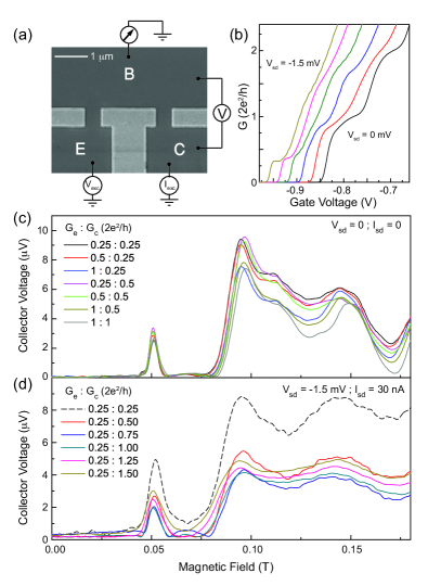
Both the emitter and collector show one-dimensional conductance quantisation and a source-drain voltage induced plateau at at chen_apl08 , as shown in Figure 1(b). The measured focusing peaks are shown in Figure 1(c) when the emitter and collector are set at the described values of conductance for . Focusing peaks appear periodically, at intervals of T, which is consistent with the cyclotron motion calculated from the two-dimensional electron concentration. The height of the focusing peaks, as anticipated, barely changes with decreasing conductance of both emitter and collector from to , indicating that there is no change in their spin polarization, i.e., and/or . As expected the peak height is independent of and for constant current injected from the emitter point contact.
When a dc bias is applied across the emitter and collector the focusing peak exhibits very different behaviour to that previously observed at zero bias. In Figure 1(d), the focusing peaks are shown for various when is fixed at , and when the dc biases across the emitter and collector were set at mV and nA, respectively. It was observed that the peak height barely changes with decreasing from to , but rises considerably when this approaches , i.e., where the anomalous plateau is found as shown in Figure 1(b). This substantial rise is predicted by Equation (1), if there is an increasing degree of spin polarization in both the emitter and collector.
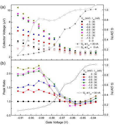
Figure 2(a) shows the height of the first peak as both the dc biases and the collector conductance were varied with the emitter conductance locked at ; this peak was chosen for investigation because of its robust structure and is seen to stay fairly constant at V, essentially independent of both and , when . However, in the low conductance region when , and nA, the focusing peaks increase as the dc bias is increased, negatively, from and then saturates when is near mV. The focusing peaks at mV are approximately twice the value of those at for every individual value of collector conductance below . This, according to Eq. (1), implies that both emitter and collector are fully spin polarized, i.e., . The saturation of the peak height is also consistent with the fact that both and cannot be larger than 1.
To further verify this bias-induced spin polarization, was decreased from 30 nA to 0 with still at mV. Figure 2(a) shows that the height of the focusing peaks drops back to almost the same value obtained when and nA as well as when both and are zero. This is again expected when either polarizer or analyzer are spin degenerate (i.e., either or equals 0). Finally, it is important to note that the value of source-drain bias mV at which the focusing peak height saturates is consistent with the bias at which the 0.25 anomaly appears, as shown in Figure 1(b).
The evolution of the focusing peaks as a function of conductancenote1 is also shown in Figure 2(a), the focusing peak rises as is reduced below , but the manner of the increase varies for different dc source-drain biases. At and nA, the peak voltage barely increases until is reduced below , in the near-pinch-off region, whereas at and nA the peak voltage starts to increase once is reduced below . The near-pinch-off increase in peak voltage with the reduced value of could be attributed to an -dependent enhancement; this has been suggested previously when is lowpotok_prl02 although the origin is not clear.
To remove nonspin related effects from the focusing peak, all the peak voltages are normalized by the values at and nAnote2 . Figure 2(b) shows the normalized peak ratio, proportional to , and the corresponding conductance as a function of gate voltage, with set to 30 nA and swept from 0 to mV. As seen the peak values rise with reducing conductance and then saturate when reaches the region of the 0.25 plateau, suggesting that has reached its maximum value of 1. Similarly, the peak ratio in the 0.25 regime rises with increasing source-drain bias applied across the emitter and then saturates. This reaches a value of , at mV when the 0.25 feature appears in the emitter conductance.
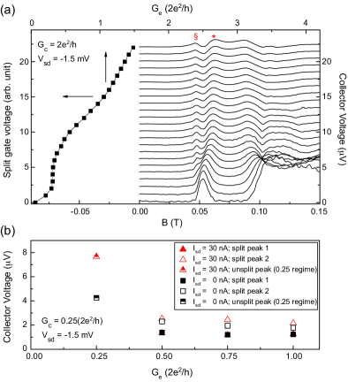
Such focusing peak enhancement was further verified by another set of measurement where was locked at as both the dc biases and were varied. Figure 3(a) shows that the focusing peak splits when the emitter conductance is above the plateau, indicating that both the source and the drain chemical potential have reached a 1D subband. The two split peaks represent focusing electrons with the source and the drain potential, respectively, whereas in the 0.25 and zero-bias regions no splitting occurs because there is only one potential across the 1D subband.
Indeed the peak enhancement, which is the evidence of spin polarization, occurs only when both and are in/below the bias-induced 0.25 plateau. Figure 3(b) clearly shows that the split focusing peaks barely changes with [only when ] and when is locked at . The enhancement only occurs when and the source-drain bias is applied. In addition, it is noteworthy that the spin-polarized plateau is very robust, nearly independent of temperatures up to K.
These results show that the emitter is functioning as a spin polarizer and the collector as a spin analyzer, demonstrating that a manipulation of the degree of polarized spin current can be achieved by tuning the source-drain bias at low values of conductance. For instance, Figure 2(b) shows that the spin polarization of the injecting current was when the emitter was set to mV and , whereas reaches for mV. We note that in the region of the 0.7 anomaly, which is found in the absence of bias, the enhancement of the peak height will be and difficult to observe unambiguously.
The effects observed here indicate that the non-equilibrium electron energy distribution and the spin coherence are maintained during the focusing transit into the collector. The transit time is sufficiently short (approximately 20 picoseconds) that phonon emission is not occurring to any significant degree, so allowing all the emitted electrons to enter the collector. The spin coherence length exceeds the path length so that the spin polarization is maintained during the focusing which augurs well for applications of this phenomenon.
Our experiments establish a link between spin and momentum which is unusual in the system with weak spin-orbit coupling. It seems most likely that the cause of the 0.25 is that a spin polarized stream of electrons is the lowest energy configuration; this configuration is retained as there is only one direction of momentum and an absence of spin scattering by electrons with the opposite momentum. A physical mechanism based on exchange interaction has recently been proposed for the 0.25 anomaly which explains the lifting of the spin degeneracylind_prb11 in the regime of non-equilibrium transport. How such exchange induced spin polarization is retained, or enhanced, by an absence of momentum degeneracy is puzzling. However, for practical applications, it is now possible to vary the degree of spin polarization in a way not previously possible. A complex arrangement of gates and applied voltages can be utilized for on-chip spin manipulation with applications in spintronics and quantum information processing.
Acknowledgements
We thank L.W. Smith, K.-F. Berggren, and C.-T. Liang for useful discussions. For technical assistance, we thank D. Anderson and S.-J. Ho. This work was supported by the Engineering and Physical Sciences Research Council (UK), EU Spinmet, and the National Science Council (Taiwan). I.F. acknowledges support from Toshiba Research Europe.
References
- (1) I. Zutic, J. Fabian, S. Das Sarma, Rev. Mod. Phys. 76, 323-410 (2004).
- (2) A. Fert, Rev. Mod. Phys. 80, 1517–1530 (2008).
- (3) Y. K. Kato, R. C. Myers, A. C. Gossard, D. D. Awschalom, Science 306, 1910–1913 (2004)
- (4) M. Konig et al., Science 318, 766–770 (2007).
- (5) D. Hsieh et al., Nature 452, 970–974 (2008).
- (6) S. M. Frolov et al., Nature 458, 868–871 (2009).
- (7) P. Debray et al., Nature Nanotechnology 4, 759 (2009).
- (8) C. H. L. Qua et al., Nature Physics 6, 336 (2010).
- (9) G. Schmidt et al., Phys. Rev. B 62, R4790 (2000).
- (10) T. J. Thornton, M. Pepper, H. Ahmed, D. Andrews & G. J. Davies, Phys.Rev.Lett. 56, 1198 (1986).
- (11) K. J. Thomas et al., Phys. Rev. Lett. 77, 135 (1996).
- (12) A. P. Micolich, J. Phys.: Condens. Matter 23, 443201 (2011).
- (13) N. K. Patel et al., Phys. Rev. B 44, 10973 (1991).
- (14) T.-M. Chen et al., Nano Lett. 10, 2330-2334 (2010).
- (15) N. K. Patel et al., Phys. Rev. B 44, 13549 (1991).
- (16) K. J. Thomas et al., Phil. Mag. B 77, 1213 (1998).
- (17) A. Kristensen et al., Phys. Rev. B 62, 10950 (2000).
- (18) R. de Picciotto, L. N. Pfeiffer, K. W. Baldwin, K. W. West, Phys. Rev. Lett. 92, 036805 (2004).
- (19) H. Kothari et al., J. Appl. Phys. 103, 013701 (2008)
- (20) S. Ihnatsenka, I. V. Zozoulenko, Phys. Rev. B 79, 235313 (2009).
- (21) T.-M. Chen et al., Appl. Phys. Lett. 93, 032102 (2008).
- (22) R. M. Potok, J. A. Folk, C. M. Marcus, V. Umansky, Phys. Rev. Lett. 89, 266602 (2002).
- (23) J. A. Folk, R. M. Potok, C. M. Marcus, V. Umansky, Science 299, 679-682 (2003).
- (24) L. P. Rokhinson, V. Larkina, Y. B. Lyanda-Geller, L. N. Pfeiffer, K. W. West, Phys. Rev. Lett. 93, 146601 (2004).
- (25) L. P. Rokhinson, L. N. Pfeiffer, K. W. West, Phys. Rev. Lett. 96, 156602 (2006).
- (26) Differential conductance of the collector was measured at a constant current.This prevents the one-dimensional channel from being fully pinched off. When the dc bias current is high ( nA) the lowest conductance is and consequently a 0.25 plateau is not observed although the spin polarization is identical. Also note that at a fixed dc current bias, , the corresponding dc voltage bias varies with the conductance.
- (27) The collector differential conductance at a particular gate voltage is dependent on source-drain bias and, therefore, normalization is not possible for different .
- (28) H. Lind, I. I. Yakimenko, & K. F. Berggren, Phys. Rev. B 83, 075308 (2011).