Synthesis of highly confined surface plasmon modes with doped graphene sheets in the mid-infrared and terahertz frequencies
Abstract
We investigate through analytic calculations the surface plasmon dispersion relation for monolayer graphene sheets and a separated parallel pair of graphene monolayers. An approximate form for the dispersion relation for the monolayer case was derived, which was shown to be highly accurate and offers intuition to the properties of the supported plasmon mode. For parallel graphene pairs separated by small gaps, the dispersion relation of the surface plasmon splits into two branches, one with a symmetric and the other with an antisymmetric magnetic field across the gap. For the symmetric (magnetic field) branch, the confinement may be improved at reduced absorption loss over a wide spectrum, unlike conventional SP modes supported on metallic surfaces that are subjected to the trade-off between loss and confinement. This symmetric mode becomes strongly suppressed for very small separations however. On the other hand, its antisymmetric counterpart exhibits reduced absorption loss for very small separations or long wavelengths, serving as a complement to the symmetric branch. Our results suggest that graphene plasmon structures could be promising for waveguiding and sensing applications in the mid-infrared and terahertz frequencies.
pacs:
73.20.Mf,73.25.i,78.66.-wI introduction
Surface plasmons raether (SPs) are charge density waves propagating at the interface between a conductor and a dielectric medium. SPs are transverse-magnetic (TM) polarized with modal fields that peak at the interface and decay exponentially away into both media. Noble metals such as gold and silver have traditionally been the material of choice to support SPs, providing for lossy but well-confined plasmon fields at visible frequencies. To achieve SP resonance in the near-infrared regime and beyond, metallic films corrugated with nanoholes spoof or nanorods, kabashin and multi-layered metmaterial structures elser ; ganol have been proposed. More recently graphene, a single layer of carbon atoms gathered in honeycomb lattice, has also been considered for supporting surface plasmon modes ranaieee ; jablanprb80 ; engheta ; mceuen ; abajoacsn12 at infrared and terahertz frequencies. The transport properties of graphene can be readily tuned by application of a gate voltage novo666 ; schedin , opening the possibilities to various plasmonic devices engheta ; ferrarinphot ; koppens ; junatnano ; avouris . Moreover, several techniques have been proposed to experimentally realize the excitation of plasmons on graphene efimovprb84 ; basovnl11 .
The SP dispersion of isolated monolayer graphene ( thick) and monolayer graphene deposited on dielectric substrates have been studied by several authors. hansonjap103 ; wunschnjp ; sarmaprb75 The plasmon dispersion for parallel graphene pairs, sarmaprb75 ; sarmaprb80 multilayer graphene stack, falkovskyprb76 and intercalated graphite shungprb34 have also been theoretically investigated. For a parallel pair, the geometry approaches the bilayer graphene when their separation is small (few angstroms), and effects of interlayer hopping could become important borghiprb80 ; sarmaprb82 .
The transport properties of graphene can be modeled with the linear response theory(Kubo formula). hansonjap103 ; falkovskyprb76 ; tobiasprb78 ; gusyninprb75 In the nonlocal random phase approximation (RPA), analytical expressions that are valid for arbitrary frequency and plasmon propagation wave vector may be derived in the limit of zero temperature. ranaieee ; wunschnjp ; sarmaprb75 ; borghiprb80 ; sarmaprb82 Alternatively in the local limit where spatial dispersion effects are negligible, falkovskyprb76 i.e., and , analytical expressions for the optical conductivity () of graphene can be obtained from the Kubo formula for finite temperatures . Here is a phenomenological electron relaxation time, is the Fermi velocity, and = . As dynamic control of the SP dispersion holds potential promise for the design of various active devices such as optical switches and modulators, it is important to study the characteristics of the SP modes such as their confinement and spatial distribution of dominant field components, so as to gain further understanding of their physical properties. In this work, further to analyzing the SP dispersion, we describe within the framework of electromagnetic waveguide theory, how the properties of the SP modes supported on monolayer graphene and parallel graphene sheets may be tuned over a broad range of frequencies for potential waveguide applications. The characteristics of the SP modes are analyzed through their associated electromagnetic mode profiles. In addition, we introduce a figure-of-merit (FOM), which in our opinion represents an optimal measure that takes into account the compromise between confinement and propagation loss of the supported SP modes to quantify the performance of the waveguide.
To describe the transport properties of graphene in our study, we calculate the local conductivity of graphene from the Kubo formula. Let us define the effective index of the supported plasmon mode as , where and is the free-space wavelength. In the local limit (), the condition translates to ( being the speed of light in vacuum), and the expression for is gusyninprb75 ; falkovskyprb76
| (1) |
where is the Fermi-Dirac distribution with as the chemical potential. In Eq. (I), the first term corresponds to contributions from intraband electron-photon scattering and the second term arises from contributions due to direct interband electron transitions. Integration of the first term leads to falkovskyprb76
| (2a) | ||||
| (2b) | ||||
For the interband term, we obtain, after evaluating the numerator of the integrand
| (3a) | ||||
| (3b) | ||||
where , and . For finite values of , the integrand in Eq. (3a) has no poles along the real axis, and is suitable for numerical integration. For , Eq. (2b) shows that is directly proportional to the chemical potential , while Eq. (3b) shows that diverges logarithmically for . Furthermore, jumps by an amount of at the interband threshold , evident of strong absorption loss for . At high frequencies, the graphene conductivity approaches a constant , which is close to the measured minimum conductivity value of geimnat438 ; sarmapnas .
For all following calculations, it is taken that (room temperature, ), and that . In this limit, Eq. (2b) and Eq. (3b) for the optical conductivity of graphene holds, and the relationship between the chemical potential and the carrier density on the monolayer graphene is
| (4) |
Since carrier density of up to has been realized in experiments yepnas108 ; efetov , we set the range of chemical potential to . Based on measured values of the carrier mobility novo666 ; efetov ; schedin which ranges from , the relaxation time is taken to be in the order of . In graphene, effects of free carrier absorption yucardona must be taken into account for photon energies above the optical phonon energy lazzeriprb73 but below . For , conservation of momentum for the free carrier absorption process can be satisfied with the emission of an optical phonon, leading to a significant decrease jablanprb80 in the relaxation time . A faster relaxation time corresponds to higher absorption losses, i.e., an increase in . The analytical expressions above for (Eqs. (I)–(3)) hold for electron and hole bands which exhibit a linear energy dispersion relation near the zero bandgap points in graphene falkovskyusp . The range of energy for which this linear dispersion relation is valid extends well into the visible spectrum, as shown by a recent experiment nairsci320 . To stay within the regime for which our analysis is valid, we limit the calculation of the graphene conductivity with Eqs. (2) and (3) to wavelengths in the range (near-infrared to terahertz regime). For long wavelengths, the conductivity is dominated by the intraband term, with the real and imaginary part scaling as and , respectively, in accordance with Eq. (2b). The conductivity decreases with wavelength until it approaches the interband threshold, where , and becomes negative. When is negative, TE (transverse electric)-polarized surface modes hansonjap103 ; zieglerteprl can be supported on graphene. This mode, whose dispersion lies close to the light line, will not be further discussed here. Instead we focus on the TM plasmon modes, which offers the potential for smaller effective mode areas compared to the noble metals, especially in the long wavelength regime where SPs supported on metals are known to be poorly confined.
The remainder of this paper is organized as follows. In Sec. II, the simplest case where monolayer graphene is sandwiched between two dielectric half-space () is re-visited. It is shown that only the antisymmetric mode (labeled as the A mode) is supported in the case when and are lossless dielectrics. By antisymmetric, we mean that the tangential magnetic field component exhibits a zero across the monolayer graphene. An approximate form for the dispersion relation for the monolayer case is derived, which is shown to be highly accurate and offers intuition to the properties of the supported plasmon mode. The case of two layers of monolayer graphene with identical chemical potential () separated by a thin dielectric medium () of thickness is investigated in Sec. III, where the separation is exploited as an additional degree of freedom to tune the properties of the SP modes. For the fully symmetric geometry () and when are purely real, the SP dispersion splits into a symmetric AS branch, and an antisymmetric AA branch, where the first A in each label refers to the antisymmetric magnetic field distribution across each monolayer graphene. The second label S (A) refers to the mode with symmetric (antisymmetric) magnetic field across the dielectric medium separating the graphene pair. The variation of the SP dispersion with wavelength (), chemical potential (), and the dielectric constant of the separating medium (), will be examined. The influence on the dispersion for an asymmetric geometry where the chemical potential on each graphene monolayer is different, will also be discussed. Finally, we offer concluding remarks in Sec. IV.
II SP modes on monolayer graphene
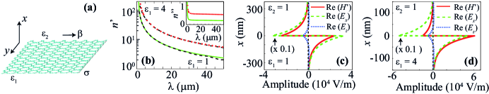
To begin, we analyze the case where monolayer graphene (at ) is sandwiched between two dielectric media () as shown in Fig. 1(a). For a guided wave with wavenumber propagating along the axis, the tangential component of -field along the axis can be expressed as
| (5) |
where is a normalization constant such that the mode has unity Poynting flux at , and
| (6) |
Here we suppress the time dependence for notation brevity. The electric field components, evaluated from Maxwell equations are
| (7a) | ||||
| (7b) | ||||
At , the continuity of the tangential electric field () yields
| (8) |
and the boundary condition for the tangential magnetic field, i.e., unit vector along ) leads to or
| (9) |
On substituting Eq. (8) into Eq. (9), we arrive at the dispersion relation
| (10) |
The dispersion relation (10) bears a striking resemblance with that for the SPs at a metal-dielectric interface. If either one of the dielectric media is a metal, then it is clear that the SP mode is almost identical to that for the metal-dielectric interface since lies in the range and is in the range . We have verified this fact numerically, which is consistent with experimental observations where carbon-on-gold substrates are used to improve the stability in SP resonance detection of DNA arrays lockett . Because of the similarity to the classical metal-dielectric interface, the metal-graphene-insulator case is not interesting in the present context and we shall focus only on the insulator-graphene-insulator (I-G-I) structure. To aid in the analysis, we note that the intraband conductivity of graphene takes the form similar to the Drude model for free electrons, i.e., , and define an effective plasmon frequency
| (11) |
where is the effective mass of the Dirac fermions geimnat438 , and is the effective thickness of the monolayer graphene. For graphene, serves as an estimate of the plasmon resonance frequency. As opposed to metals with parabolic electron dispersion where the plasmon frequency is proportional to , for graphene. junatnano ; sarmaprb75 Let us note that in Eq. (II) is not necessarily the physical thickness of the graphene layer, rather it is the effective thickness that would allow us to recover the correct dispersion relation when the monolayer graphene is treated as a thin metal film or screening layer. To estimate , we take , which gives for .
Far from the plasmon resonance frequency, the loss of the bound modes or equivalently the imaginary part of the wavenumber () is small. Consequently, Eq. (6) implies that the imaginary part of is small compared to the real part (), and . As must be positive for the bound modes, Eq. (8) implies that the -field must change sign across the monolayer graphene when both the adjacent media are lossless dielectrics, and hence only the antisymmetric mode (labeled A) is supported in the case of the I-G-I. Taking and , the real part of the SP mode effective index () for and 4 is shown in Fig. 1(b). Following the derived results of Ref. [21], we have also calculated the SP dispersion relation with the nonlocal RPA, which shows a good agreement with Eq. (10) (see black-dashed curves in Fig. 1(b)). Similar to the antisymmetric SP modes supported on thin metal films, it is seen that . As , increases rapidly. The electromagnetic field components for and , are shown in figs. 1(c) and 1(d) respectively, taking and as an example. It is evident that the -field of the A mode switches sign across the monolayer graphene, and has a maximum at the side of the dielectric with a higher permittivity (if . It is worth noting that because is relatively large compared to , the magnitude of the normal and tangential field components are comparable raether according to Eq. (7), i.e., . This is in contrast to SP modes supported on metal-air interfaces that have , and have the normal electric field component as the dominant field component. For cases where the wavenumber of the SP supported on monolayer graphene satisfy , one should be able to make the approximation (see Eq. (6)), which remains accurate provided and . Substituting the approximation into Eq. (10) yields a simple and physically intuitive solution
| (12) |
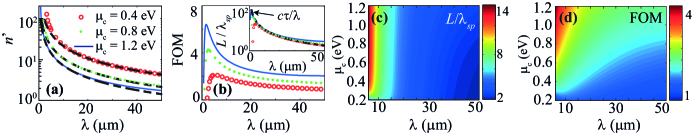
where , and the substitution has been made in the last step. jablanprb80 Separating Eq. (II) into real and imaginary parts, we find , and . This gives us some insight to the physical characteristics of the A mode. First, similar to the case of SPs supported on metal films, the A mode is better confined (larger ) for higher values of or (as seen in Fig. 1(b)), accompanied with a proportional increase in absorption loss (larger ). Second, varies as , decreasing at a rate much faster than which varies as . Therefore, where the approximation is valid, varies as and is constant, in agreement with the dispersion curves of Fig. 1(b). Third, a higher doping level decreases the confinement, which can be understood because the graphene becomes more like a perfect conductor with increased conductivity (see Eq. (2b)) and supports SP modes whose fields extends more into the dielectric media. This trend is shown in Fig. 2(a) with the case of isolated monolayer graphene (), where for different values of is shown. It can be seen that the approximate solution Eq. (II) is in excellent agreement with the exact dispersion relation (10) except near the plasmon resonance frequency. For antisymmetric A modes well-described by the approximation (II), the normalized propagation length at which the field amplitude of the SP falls to of the initial value is jablanprb80
| (13) |
which depends only on the operating wavelength and relaxation time . As seen from the inset of Fig. 2(b), the approximate form remains highly accurate for operating wavelengths up to . The slight deviation for is attributed to the inequality in the approximation (II), as the inequality is less accurate for longer wavelengths since as explained, and . The peak value of is seen to increase with according to the curve because a higher chemical potential has the effect of blue-shifting , see Eq. (II). It is worthwhile noting that the ratio can also act as a figure-of-merit (FOM) for 1D plasmonic waveguides, beriniopex and is shown in Fig. 2(c) for as a function of wavelength. However, in the case of graphene, is virtually independent of important parameters like and (see Eq. (13)). As such we propose an alternative FOM,
| (14) |
where the propagation length of the SP is normalized by the geometric mean of its effective wavelength and the free-space wavelength. The FOM as defined in Eq. (14) for as a function of wavelength is shown in Fig. 2(d). In contrast to the ratio , the FOM is clearly distinct for different values of the chemical potential and wavelength. As such, we propose the newly defined FOM as a measure of the performance of graphene plasmon waveguides. For the graphene pair studied in the next section, this FOM will also be applied to quantify its performance as a SP waveguide.
III Tuning the SP mode with a pair of parallel graphene layers
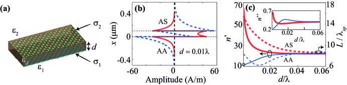
Next, we demonstrate how one may tune the confinement and propagation characteristics of the SP mode by introducing an additional layer of graphene. Here, two monolayers of graphene (at ) are separated by a thin dielectric medium () as shown in Fig. 3(a). Let us neglect the effects of absorption losses due to coupling with optical phonons () as described in Sect. I and consider the range of wavelengths . We are primarily concerned with graphene pairs whose spatial separation is sufficiently large such that effects of interlayer hopping, which can be important for closely-spaced graphene pairs (few angstroms apart) or bilayer graphene, have no significant bearing on the SP dispersion. sarmaprb82 For the following analysis, the smallest separation we consider is , i.e. .
For a parallel pair of graphene monolayers separated by a distance , the tangential -field in each of the dielectric media can be expressed as
| (15) |
where is a normalization constant similar to in Eq. (5). Matching the boundary conditions at and , we obtain for the tangential -field
| (16a) | ||||
| (16b) | ||||
and for the tangential component,
| (17a) | ||||
| (17b) | ||||
where . In Eq. (16), and are the conductivities of the graphene monolayers at and . The graphene conductivities and , which are calculated with Eq. (I), may be tuned through their respective chemical potentials and . Eliminating and from Eqs. (16) and (17) yields the dispersion relation
| (18) |
with
| (19) |
In the symmetric case where and , the dispersion relation (18) splits into two branches
| (20a) | ||||
| (20b) | ||||
where due to symmetry. Let us take the case , which is a configuration that has also been studied in the context of Casimir forces woodsprb82 and quasi-transverse electromagnetic waveguide modes hansonjap104 . Unless otherwise specified, it will be taken that the geometry is fully symmetric with , and .
For large separations of the graphene pair, both Eqs. (18) and (20) reduce to the dispersion relation (10) for the case of the I-G-I. For sufficiently small such that the SP supported on individual graphene monolayer interacts with each other, the dispersion splits into an even and an odd mode. The typical field distribution of the -field for these two modes are shown for , , and as an example in Fig. 3(b). The field displays a symmetric (antisymmetric) character across the gap for the even (odd) mode. Consistent with the analysis for monolayer graphene in Sect. II, the field is antisymmetric across each graphene layer. As such, let us label the even mode AS and the odd mode AA, where the first A in the labels refers to the antisymmetric -field distribution across each graphene monolayer. Additionally, let us note that the other two branches SA and SS (the first label S refers to the symmetric -field across the graphene), can also be supported when the dielectric layer is a thin metal film. tamir This case is verified with numerical simulations (not shown), where it was found that, similar to the case of the I-G-I, the dispersion with and without the graphene films differ only marginally. As such, we focus on the I-G-I-G-I structure.
Figure 3(c) illustrates the splitting of the SP dispersion into the AA (thin blue curves) and AS (thick red curves) modes as the separation is decreased, for the case and . Notice the difference in the vertical scales for and . For sufficiently large , both the AA and AS branches merge to the A mode supported by the monolayer graphene. As the separation is decreased, the real part of the effective index increases (decreases) monotonically for the AS (AA) branch, corresponding to improved (degraded) confinement of the SP mode. On the other hand, the imaginary part of the effective index (inset of Fig. 3(c)) for both modes exhibits a nonmonotonic behavior. While this nonmonotonic behavior is also observed in the normalized propagation length for the AA branch (dashed blue curve), it is absent for the AS branch (dashed red curve) however. This is because the SP wavelength decreases more quickly than the absorption loss increases as is decreased. At very small separations , or equivalently long wavelengths , the AS branch would be strongly suppressed due to the exponential increase in absorption.
For the AA mode, it is expected, within linear optics, that the amplitude of the -field across the dielectric gap () approaches asymptotically to a saw-tooth waveform with a near-zero amplitude as the separation decreases (see Fig. 3(b)). This implies that the electromagnetic field in the gap is squeezed out of the gap into the two dielectric half-space as decreases, explaining the decrease in the confinement () in Fig. 3(c). In the limit , the AA mode tends to the A mode for the case of the bilayer graphene. fnote1 Here we estimate the conductivity of the bilayer graphene to be twice the conductivity of the monolayer, following the approximation for few layer graphene, ferrarinphot ; hansonjap104 ; ferrarinl where is the number of layers . In Fig. 3(c), it is seen that for the AA branch approaches that of the bilayer case, marked with a circle on the vertical axis. For and , the SP dispersion of the monolayer graphene satisfies the condition (see Fig. 2(a)), and thus for the bilayer case and monolayer case are almost equal (see inset Fig. 2(b)). These observations are all in agreement with the data for the AA mode represented by the blue curves in Fig. 3(c). For the AS mode, as long as the separation is not too small ( for this example), the increase in the confinement is accompanied with reduced absorption loss (). This concomitant improvement in confinement and absorption loss, which is contrary to the trade-off between confinement and loss associated with conventional SP modes, bozhenphot is also observed for SPs supported in dielectric-loaded metallic waveguides bozheprb75 that exhibit similar dispersion characteristics as the AS mode.
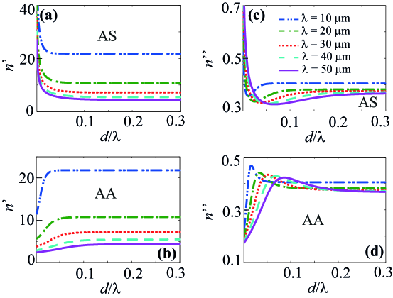
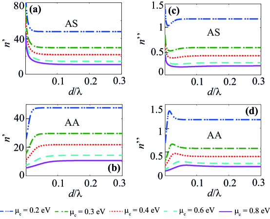
The influence of the operating wavelength () and chemical potential () on the dispersion of the AA and AS modes are shown in Figs. 4 and 5, respectively. As observed, the behavior of the AS and AA branches share a number of similar characteristics with the case of the monolayer graphene investigated above. Let us first focus on the influence of the wavelength (Fig. 4), where the chemical potential is taken to be . For both branches, Figs. 4(a) and 4(b) show that is inversely proportional to , whereas changes only weakly for different wavelengths (Figs. 4(c) and 4(d)). The result is an overall decrease in the normalized propagation length as increases. Additionally, because an increased wavelength effectively decreases the separation , the two branches begin to merge for larger values of the normalized separation .
Figure 5 shows the influence of the chemical potential on the dispersion of the two modes, where the wavelength is taken to be . Both (Figs. 5(a) and 5(b)) and (Figs. 5(c) and 5(d)) decreases as increases, i.e., a higher chemical potential increases the conductivity of graphene, thereby reducing the confinement and the absorption loss. For a higher value of the chemical potential, because of the longer effective SP wavelength (), the separation between the graphene pair is effectively decreased, and thus the two branches start merging at larger separations . A common feature of all the dispersion curves in Figs. 4 and 5 is that the change in or becomes increasingly less profound as or increases. These behaviors suggests an inversely proportional relationship between the wavenumber of each SP mode (AA or AS) and or , in a similar fashion to Eq. (II) for the monolayer case in Sect. II. From the above observations, the influence of on the dispersion curves of the two modes may also be inferred. Since increasing has the same effect of reducing the effective SP wavelength , the behavior for a greater dielectric constant of the separating medium () is qualitatively similar to a lower value of the chemical potential. As such, the AS and AA branches would merge for smaller separation for a higher value of (with all other parameters kept constant). Similar to a lower chemical potential, a higher would result in a higher maximum value of . These behaviors for different values of have been verified with calculations (not shown) .
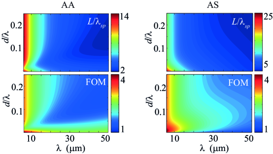
Next, let us compute the FOM as defined in Eq. (14) for the AA and AS modes. We shall make a comparison between the FOM and the ratio to see if the newly-defined FOM serves better to quantify the performance of the two modes for waveguiding operation. The two quantities and FOM for the two modes as a function of the normalized separation and wavelength are shown in Fig. 6, with the chemical potential taken to be . Except for a narrow region confined to and , Fig. 6 (top panels) reveals that the ratio varies only very weakly with for a given wavelength. Furthermore, the ratio fails to highlight the fact that the AS mode is extremely lossy for small separations . By looking at the top panels of Fig. 6, one might also be misled to believe that the AA and AS modes are not useful for waveguiding operation for the long wavelengths in the terahertz regime. These deficiencies are circumvented with the corresponding FOM shown in the bottom panels of Fig. 6. First, let us note that unlike the ratio , the FOM of the two modes for a given set of parameters lie in a similar range of values (see the scale on the colorbars). This is due to the factor in the FOM of Eq. (14) instead of in the ratio . Second, the FOM of the AA mode for very small separations , or equivalently long wavelengths, can be relatively high. This is due primarily to the smaller absorption loss as the AA mode tends to the bilayer case. On the other hand, the AS mode provides a better FOM for intermediate values and . Thus for a properly chosen separation , the parallel graphene pair offers at least one plasmon mode that is suitable for waveguide operation over the mid-infrared and terahertz spectrum. For a higher (lower) , the absorption loss decreases (increases), confinement degrades (improves), and the general trend is an increase (decrease) in the FOM with the two branches starting to merge at larger (smaller) separations .
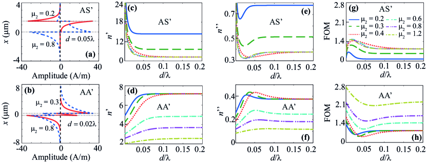
So far we have considered fully symmetric geometries. Yet another degree of freedom to tune the SP dispersion of the two branches is to control the chemical potential of one of the graphene monolayer while keeping the other one fixed. Evidently when , the symmetry is broken, and the fields of the modes no longer obey even or odd symmetry (see Figs. 7(a) and 7(b)). As such, let us define new branches AS’ and AA’ that stem from the AS and AA modes (respectively) for the symmetric case where . As an example, let us take that is fixed with adjustable for an operating wavelength . For this case, the two modes for which are the AA and AS modes, whose dispersion has been given in Fig. 4 (red dotted curves). The influence on the dispersion when is varied so that and are no longer equal is shown in Figs. 7(c) to 7(f). To aid the analysis, let us further categorized the dispersion behavior of the AS’ and AA’ branches for and . For the AS’ (AA’) branch, the dispersion is only weakly influenced for (), but changes visibly for (). Figures 7(c) and 7(d) show that generally decreases for increasing for both branches, consistent with earlier analysis on the AA and AS modes (see Figs. 4 and 5). As observed in Figs. 7(e) and 7(f), the dispersion of for the AA’ and AS’ branches exhibits a non-monotonic behavior, also similar to their symmetric counterparts. For the AS’ branch with and the AA’ branch with , both and decrease for increasing as expected.
The dispersion behavior is however a little different for the weakly influenced case. In this case, for a qualitative explanation of the dispersion, let us take the AS’ (AA’) branch with () to be a mode that has characteristics dominant of the AS (AA) mode but with a slight perturbation due to contribution from the AA (AS) mode, i.e., the two modes are mixed but with a dominant AS or AA character. For the AS’ branch, is decreased very slightly for increasing for . In the range the AS’ mode is modified with contributions from the more lossy AA mode, thus the absorption loss is increased even for . For the AA’ branch, is increased slightly for decreasing for . In the range the AA’ mode is modified with contributions from the less lossy AS mode, thus decreasing the absorption loss for .
We have shown the typical mode profile for the AS’ and AA’ modes for in Figs. 7(a) and 7(b). In agreement with the analogy of the mixed mode, it is seen that the case of the weakly influenced dispersion ( for AS’ given in dashed blue curve of Fig. 7(a) and , for AA’ given in solid red curve of Fig. 7(b)) displays a relatively stronger AS or AA behavior. On the other hand, the solid red curve in Fig. 7(a) () resembles that of the A mode (for monolayer graphene) with very little influence from the other graphene layer, and the dashed blue curve in Fig. 7(b) () also resembles that of the A mode but slightly split within the graphene pair. A complete understanding of the physical mechanism leading to the weakly dispersive behavior of the AS’ and AA’ modes for the somewhat contrasting conditions described above is a future topic of investigation. The above analysis also shows that, while an asymmetric chemical potential generally increases the absorption loss for the AS’ branch, it may serve to reduce the absorption loss for the AA’ branch quite significantly. The corresponding FOM for the two branches are shown in Figs. 7(g) and 7(h), where it is seen that the dispersion characteristics described above are well-captured with the FOM. While the highest FOM is associated with the AA’ branch for large values of (), the lowest FOM is observed for the AS’ branch for small values of ().
IV Conclusion
In summary, for this article we have revisited the plasmon disperison in monolayer graphene, followed by a thorough investigation of the dispersion of the SP modes supported in a parallel pair of graphene monolayers separated by a distance . Due to the matching of boundary conditions across the interface of the monolayer graphene, it is found that the I-G-I combination supports only the A mode (antisymmetric magnetic field across the monolayer). To quantify the waveguiding performance of the SP mode, we found that a newly-defined FOM is more optimal than the ratio because for a wide spectral range for which the approximation (II) is satisfied, the latter is almost independent of important parameters such as the chemical potential and dielectric constants of the neighboring media.
In the case of the graphene parallel pair, the separation is employed as an additional degree of freedom to tune the SP dispersion. For the fully symmetric geometry, the dispersion for the graphene pair splits into an even AS and odd AA branch for sufficiently small separations . While the AS and AA modes may be characterized based on the symmetry of each mode, they share similar characteristics as the A mode supported in monolayer graphene. For instance, the influence of the wavelength and the chemical potential on the dispersion of the AS and AA modes are similar to that of the A mode in monolayer graphene, i.e. their wavenumbers are somewhat inversely proportional to the wavelength and chemical potential, similar to Eq (II). The non-monotonic behavior of the absorption loss () means that there exist a certain range whereby the AS and AA modes are less absorptive compared to the monolayer case. By calculating the FOM, it is seen that the AA mode is optimal for small separations or equivalently, long wavelengths . On the other hand, the AS mode offers a better FOM than the AA mode for an intermediate range of separations and wavelengths where it is both less absorptive and better confined. For very small however, the AS mode is strongly suppressed as its absorption increases exponentially. It is noted that the AA and AS branches here correspond to the optical and acoustic plasmon branches (respectively) in existing literature on theoretical investigation of the plasmon dispersion relation of the parallel graphene pair. sarmaprb75 ; sarmaprb80 ; sarmaprb82 Varying the chemical potential of one of the graphene monolayers allows for yet another degree of freedom to tune the SP dispersion. Strictly speaking, the fields no longer possess symmetry in this case. However, we take the case as reference, and consider branches AS’ and AA’ that stem from the AS and AA modes respectively. Our analysis shows that, under the right conditions, an asymmetric chemical potential can significantly reduce the absorption loss for the AA’ branch. Our results demonstrate the potential to effectively tune the SP mode dispersion with a parallel pair of graphene monolayers to achieve well-confined and propagative SP modes in the mid-infrared and terahertz regime with graphene structures. This graphene plasmon waveguide platform is promising for mid-infrared and terahertz applications.
Acknowledgements
This work was supported by the Agency for Science and Technology Research (A*STAR), Singapore, Metamaterials-Nanoplasmonics research program under A*STAR-SERC grant No. 0921540098.
References
- (1) H. Raether, Surface Plasmons on Smooth and Rough Surfaces and on Gratings, (Springer, Berlin, 1988).
- (2) J. B. Pendry, L. Martín-Moreno, and F. J. Garcia-Vidal, Science 305, 847 (2004).
- (3) A. V. Kabashin, E. Pevans, S. Pastkovsky, W. Hendren, G. A. Wurtz, R. Atkinson, R. Pollard, V. A. Podolskiy, and A. V. Zayats, Nat. Materials 8, 867 (2009).
- (4) J. Elser, A. A. Govyadinov, I. Avrutsky, I. Salakhutdinov, and V. A. Podolskiy, J. Nanomat. 2007, 79469 (2007).
- (5) C. H. Gan and P. Lalanne, Opt. Lett. 35, 610 (2010).
- (6) F. Rana, IEEE Trans. Nanotech. 7, 91 (2008).
- (7) M. Jablan, H. Buljan, and M. Soljačic, Phys. Rev. B 80, 245435 (2009).
- (8) A. Vakil and N. Engheta, Science 332, 1291 (2011).
- (9) S. F. Shi, X. Xu, D. C. Ralph, and P. L. McEuen, Nano Lett. 11, 1814 (2011).
- (10) J. Christensen, A. Manjavacas, S. Thongrattanasiri, F. Koppens, F. J. García de Abajo, ACS Nano 6, 431 (2012).
- (11) K. S. Novoselov, A. K. Geim, S. V. Morozov, D. Jiang, Y. Zhang, S. V. Dubonos, I. V. Grigorieva, and A. A. Firsov, Science 306, 666 (2004).
- (12) F. Schedin, A. K. Geim, S. V. Morozov, E. W. Will, P. Blake, M. I. Katsnelson, and K. S. Novoselov, Nat. Materials 6, 652 (2007).
- (13) F. Bonaccorso, Z. Sun, T. Hasan, and A. C. Ferrari, Nat. Photon. 4, 611 (2010).
- (14) F. Koppens, D. E. Chang, and F. J. García de Abajo, Nano Lett. 11, 3370 (2011).
- (15) L. Ju, B. Geng, J. Horng, C. Girit, M. Martin, Z. Hao, H. A. Bechtel, X. Liang, A. Zettl, Y. R. Shen, and F. Wang, Nat. Nanotech. 6, 1 (2011).
- (16) P. Avouris, Nano Lett. 10, 4285 (2011).
- (17) K. A. Velizhanin, and A. Efimov, Phys. Rev. B 84, 085401 (2011).
- (18) Z. Fei, G. Andreev, W. Bao, L. M. Zhang, A. S. McLeod, C. Wang, M. K. Stewart, Z. Zhao, G. Dominguez, M. Thiemens, M. M. Fogler, M. J. Tauber, A. H. Castro-Neto, C. N. Lau, F. Keilmann, and D. N. Basov, Nano Lett. 11, 4701 (2011).
- (19) G. Hanson, J. Appl. Phys. 103, 064302 (2008).
- (20) B. Wunsch, T. Stauber, F. Sols, and F. Guinea, New J. Phys. 8, 318 (2006).
- (21) E. H. Hwang, and S. Das Sarma, Phys. Rev. B 75, 205418 (2007).
- (22) E. H. Hwang, and S. Das Sarma, Phys. Rev. B 80, 205405 (2009).
- (23) L. A. Falkovsky and S. S. Pershoguba, Phys. Rev. B 76, 153410 (2007).
- (24) K. W. -K. Shung, Phys. Rev. B 34, 979 (1986).
- (25) G. Borghi, M. Polini, R. Asgari, and A. H. MacDonald, Phys. Rev. B 80, 241402(R) (2009).
- (26) R. Sensarma, E. H. Hwang, and S. Das Sarma, Phys. Rev. B 82, 195428 (2010).
- (27) T. Stauber, N. M. R. Peres, and A. K. Geim, Phys. Rev. B 78, 085432 (2008).
- (28) V. P. Gusynin, S. G. Sharapov, and J. P. Carbotte, Phys. Rev. B 75, 165407 (2007).
- (29) K. S. Novoselov, A. K. Geim, S. V. Morozov, D. Jiang, M. I. Katsnelson, I. V. Grigorieva, S. V. Dubonos, and A. A. Firsov, Nature 438, 197 (2005).
- (30) S. Adam, E. H. Hwang, V. M. Galitski, and S. Das Sarma, Proc. Natl. Acad. Sci. 104, 18392 (2007).
- (31) J. Ye, M. F. Craciun, M. Koshino, S. Russo, S. Inoue, H. Yuan, H. Shimotani, A. F. Morpurgo, and Y. Iwasa, Proc. Natl. Acad. Sci. 108, 13002 (2011).
- (32) D. K. Efetov and P. Kim, Phys. Rev. Lett. 105, 256805 (2010).
- (33) P. Y. Yu and M. Cardona Fundamentals of Semiconductors: Physics and Materials Properties, 4th ed. (Springer, Heidelberg, 2010).
- (34) M. Lazzeri, S. Piscanec, F. Mauri, A. C. Ferrari, and J. Robertson, Phys. Rev. B 73, 155426 (2006).
- (35) L. A. Falkovsky, Physics-Uspekhi 51, 887 (2008).
- (36) R. R. Nair, P. Blake, A. N. Grigorenko, K. S. Novoselov, T. J. Booth, T. Stauber, N. M. R. Peres, and A. K. Geim, Science 320, 1308 (2008).
- (37) S. A. Mikhailov and K. Ziegler, Phys. Rev. Lett. 99, 016803 (2007).
- (38) M. R. Lockett, S. C. Weigel, M. F. Phillips, M. R. Shortreed, B. Sun, R. M. Corn, R. J. Hamers, F. Cerrina, and L. M. Smith, J. Am. Chem. Soc. 130, 8611 (2008).
- (39) P. Berini, Opt. Exp. 14, 13030 (2006).
- (40) D. Drosdoff and L. M. Woods, Phys. Rev. B 82, 155459 (2010).
- (41) G. Hanson, J. Appl. Phys. 104, 084314 (2008).
- (42) J. J. Burke, G. I. Stegeman, and T. Tamir, Phys. Rev. B 33, 5186 (1986).
- (43) Actually, the hyperbolic dispersion of the electron and hole bands and effects of interlayer tunneling for bilayer graphene should be taken into account for quantitative calculations of the plasmon dispersion, see Sensarma et al. sarmaprb82 for instance. In Ref. sarmaprb82 , it was also shown that the plasmon dispersion of the bilayer graphene would behave like monolayer graphene for carrier density , corresponding to chemical potential . For the example in Fig. 3, the carrier density is for (see Eq. (4)), and thus the system can be treated effectively as monolayer graphene with linear band dispersion.
- (44) C. Casiraghi, A. Hartschuh, E. Lidorikis, H. Qian, H. Harutyunyan, T. Gokus, K. S. Novoselov, and A. C. Ferrari, Nano Lett. 7, 2711 (2007).
- (45) D. K. Gramotnev and S. I. Bozhevolnyi, Nat. Photon. 4, 83 (2010).
- (46) T. Holmgaard and S. I. Bozhevolnyi, Phys. Rev. B 75, 245405 (2007).