Strain-tunable band gap in graphene/h-BN hetero-bilayer
Harihar Behera***E-mail: harihar@phy.iitb.ac.in; harihar@iopb.res.in and Gautam Mukhopadhyay†††Corresponding author’s E-mail: gmukh@phy.iitb.ac.in; g.mukhopa@gmail.com
Department of Physics, Indian Institute of Technology, Powai, Mumbai-400076, India
Abstract
Using full-potential density functional calculations within local density
approximation (LDA), we predict that mechanically tunable band-gap and
quasi-particle-effective-mass are realizable in graphene/hexagonal-BN
hetero-bilayer (C/h-BN HBL) by application of in-plane homogeneous biaxial
strain. While providing one of the possible reasons for the experimentally
observed gap-less pristine-graphene-like electronic properties of C/h-BN HBL, which theoretically has a narrow band-gap, we suggest a schematic experiment for
verification of our results which may find applications in
nano-electromechanical systems (NEMS), nano opto-mechanical systems (NOMS) and
other nano-devices based on C/h-BN HBL.
Keywords : Nanostructures, Ab initio calculations, Electronic structure, Transport properties
1 Introduction
Recent experiments [1, 2] at Columbia University showing the successful
fabrication of hexagonal BN (h-BN) gated graphene field effect transistors
(BN-GFETs), consisting of both mono-layer graphene (MLG) and bilayer graphene
(BLG) on h-BN gate/substrate which could be made arbitrarily thin (down to a
mono-layer of h-BN), are among the important developments in the physics and material science of graphene [3, 4, 5, 6]. Graphene supported on h-BN exhibits superior electrical
properties with performance levels comparable to those observed in suspended
samples [1, 2, 6, 7]. On the other side, in the context of strain
engineering of electronic properties of graphene, another significant
experimental development [8] utilizes piezoelectric actuators to apply
tunable biaxial compressive as well as tensile stresses to graphene on h-BN
substrate, which allows a detailed study of the interplay between the graphene
geometrical structures and its electronic properties. In this scenario, it is
useful and interesting to explore the effect of biaxial strain on the band gap, Fermi-velocity and the quasi-particle-effective-mass of a graphene/h-BN hetero-bilayer
(representing the smallest and the simplest form of BN-GFET), which is not only feasible but also desirable, since
strain-engineering [9] of Si, SiGe, Ge has been successfully used in the
semiconductor industry to impressively improve the performance levels of
conventional metal-oxide-semiconductor field-effect transistors (MOSFETs),
and recently [10] strain is seen as a solution for higher carrier mobility
in nano MOSFETs.
In this paper, we theoretically explore the effect of symmetry preserving
homogeneous in-plane biaxial strain (which mimics an experimental
condition [8] in which a flexible substrate supported graphene can be
strained in a controllable way by piezoelectric actuators) on a hetero-bilayer
(C/h-BN HBL) consisting of an MLG (C) and a mono-layer of h-BN, which is the
smallest and simplest form of BN-GFET. Previous theoretical studies on
graphene on h-BN substrate [11] and C/h-BN HBL [12, 13] reported the
opening of a small energy band gap in graphene which varies with (a) the
stacking order,
(b) the separation distance of graphene from the h-BN, and (c) the externally
applied perpendicular electric field. Other graphene/h-BN heterostructures
such as MLG [14] and BLG [15] sandwiched between two mono-layers of
h-BN have also been theoretically shown to have (external)
electric-field-tunable electronic properties. However, a detailed study of
strain-engineered band gap of C/h-BN HBL is not available, although the
effects of various strain distributions on mono-layer h-BN [16] and
graphene [17, 18, 19, 20] have been reported recently. Theoretically it is
shown that the high band gap of mono-layer h-BN is strain-tunable [16],
the gap-less nature of graphene is robust against small and moderate
deformations [17, 18, 19, 20]. On the experimental side, Raman
spectroscopy studies [8, 21, 22, 23, 24] of graphene reveal that both
biaxial [8] and uni-axial [21, 22, 23, 24] strains affect
the Raman Peaks; the transport properties of strained graphene have been
investigated by depositing samples on stretchable substrates [25].
Insights from these studies suggest a detectable strain-controlled band-gap
in a composite structure like C/h-BN HBL. This expectation has, in fact, been
borne out by the results of our present study. It is shown that the ground
state direct band gap ( meV) of C/h-BN HBL increases with biaxial
tensile strain and decreases with compressive strain, whereas the Fermi
velocity of charge carriers follows a reverse trend. Moreover, the variation
of computed average effective masses () of charge carriers
(electrons or holes) with strain is more pronounced with increasing
trend for tensile strain and decreasing trend for compressive strain.
These should affect the carrier mobility, conductivity and optical properties
of C/h-BN HBL which may be verified experimentally for which we propose
schematically a realistic experimental set-up.
2 Computational Methods
Our first-principles study of electronic structure of C/h-BN HBL is based on full-potential (linearized) augmented plane wave plus local orbital (FP-(L)APW+lo) method[26], which is a descendant of FP-LAPW method[27]. We use the elk-code[28] and the Perdew-Zunger variant of LDA[29], the accuracy of which has been successfully tested in our previous work [30] on graphene and silicene (silicon analog of graphene). The plane wave cut-off of (a.u) ( the smallest muffin-tin radius) was chosen for plane wave expansion in the interstitial region. The Monkhorst-Pack [31] point grid of is used for structural optimization and of for electronic calculations of C/h-BN BLG with simulated homogeneous in-plane biaxial strains up to . Our consideration of strains up to is motivated by recent theoretical calculations as well as experiments which demonstrated that graphene can sustain in-plane tensile elastic strain in excess of ; Kim et al. have measured resistances of graphene films transferred to pre-strained and unstrained PDMS substrates with respect to uni-axial tensile strain ranging from to . Although in-plane homogeneous biaxial strains up to have been considered theoretically in , the maximum compressive strain graphene can sustain is unclear to us. However, for the sake of symmetry and as a matter of curiosity, we have considered strains up to . The total energy was converged within eV/atom. We simulate the 2D-hexagonal structure of C/h-BN BLG as a 3D-hexagonal super-cell with a large value of -parameter ( a.u.) by considering the primitive vectors of the unit cell as
| (1) |
| (2) |
| (3) |
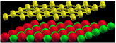
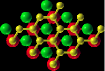
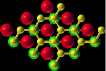
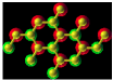
where is the in-plane lattice parameter and other symbols have their usual meanings. The value of was varied to simulate the application of homogeneous in-plane biaxial stress (since = = a) to C/h-BN HBL. Figure 1 schematically shows the structure of C/h-BN HBL in which (a) represents a typical structure, (b)-(d) represent top-down views of three different configurations.
3 Results and Discussions
Our calculated LDA lattice constants of graphene and h-BN mono-layer
respectively turned out as (C) = 2.445 Å and (BN) = 2.488 Å,
which are in excellent agreement with the reported values for graphene
((C) = 2.445 Å in Ref. (11), 2.4426 Å in Ref (17), 2.4431 Å
in Ref (37)) and mono layer h-BN ((BN) = 2.488 Å in Ref. (16), 2.4870 Å
in Ref (37)) based on plane wave pseudo-potential method. Graphene turned out
as gap-less, while mono-layer h-BN with its valence-band maximum and the conduction
band minimum located at K point of the Brillouin Zone (BZ), revealed a direct
band gap of 4.606 eV, in agreement with previous calculations of 4.613 eV in
Ref. [16], 4.35 eV in Ref. [37]. Our estimated band gap energy of h-BN mono-layer
is about 23% less than the experimental [38] direct band gap energy of
5.971 eV.
The calculations for the composite structure of C/h-BN HBL were done as
follows, unlike the earlier authors [11, 12] who used the LDA value of
lattice constant of graphene ((C)= 2.445 Å) for the
three configurations of C/h-BN HBL.
As per the previous studies [11, 12], B1 configuration of C/h-BN HBL
(henceforth we call it C/h-BN HBL(B1) or simply B1) is the most stable
configuration with equilibrium interlayer spacing (B1) = 3.22 Å at
an assumed (B1) = 2.445 Å. For B1, with which we are concerned in
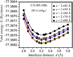
the present paper, the calculated ground state total
energies at different “” values for five fixed values of “” ( = 2.445, 2.450,
2.460, 2.470, 2.480 Å ) were obtained as depicted in Figure 2; from this
we estimated the optimized values of “” and “” as (B1) = 2.47 Å
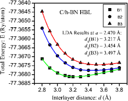
and (B1) = 3.217 Å. Similar calculations for B2 and B3 are required for
a comparison of the relative stability of B1, B2 and B3. However, like
previous authors [11, 12, 13], we got the relative stability and minimum
interlayer distance of B1, B2 and B3 at constant “” Å
as depicted in Figure 3, which corroborate the reported results[11, 12, 13].
The interlayer spacing of B2 and B3 at a common value of = 2.47 Å
were estimated as (B2) = 3.454 Å, (B3) = 3.497 Å which agree
with the reported results [11, 12] of (B2) = 3.4 Å and
(B3) = 3.5 Å.
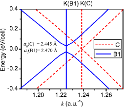
The band structures of unstrained graphene and unstrained C/h-BN HBL(B1)
near the K point of the BZ are depicted in Figure 4 for comparisons.
As seen in Figure 4, graphene is gap-less, whereas C/h-BN HBL(B1) has a
direct band gap of E= 59 meV which is of same order of
magnitude as that of graphene on a hexagonal BN
substrate [11] (E = 53 meV) in the same configuration.
Therefore, the number of h-BN layers below graphene mono-layer has little
impact on the band structure of C/h-BN heterostructure.
It is to be noted that E is under-estimated here because of the LDA.
However, in experiments involving graphene on h-BN substrates, there is
no evidence of this gap from transport measurements and this absence of gap has
been attributed to randomly stacked graphene on h-BN . The fabrication of a
graphene/h-BN heterostructure with a desired alignment seems to be a technological
hurdle at present. However, we note that Fan et al. have investigated one
type of misalignment of graphene to h-BN layer (along with the three aligned structures
B1, B2 and B3 we have considered), which they have achieved by translating BN
mono-layer a distance of ( is the lattice constant of graphene)
with respect to graphene along the C-C bond orientation from a pattern that corresponds
to the B3 configuration of our present study. This misaligned heterostructure with
an estimated equilibrium interlayer distance of Å is energetically
shown to be unstable with respect to the most stable configuration that
corresponds to the B1 configuration of our present study. Further,
this misaligned structure is pictorially shown to have a small band gap which
vanishes when the interlayer distance reaches Å. It is to be noted that the
theoretical study in is concerned with the effect of interlayer
spacings on electronic structure of graphene/h-BN hetero-bilayer and
there is no consideration of biaxial strain effects. We also note that
since our simulated homogeneous biaxial strain preserves the hexagonal
symmetry of an aligned C/h-BN HBL (say B1), a misalignment is not expected to occur
in such C/h-BN HBL under homogeneous biaxial strain which only affect the size but not the shape of the hexagonal structure under study.
The energy dispersion around K point of BZ is linear for graphene and
therefore the low energy quasi-particles mimic the massless Dirac fermion
behavior[3, 4], i.e.,
| (4) |
where is Fermi energy, is Fermi velocity of quasi-particles,
and is the momentum. In case of B1, low energy dispersion is not only linear
in but also parallel to the low energy dispersion of graphene, while very
low energy dispersion within an energy window of (-0.06 eV , +0.06 eV) around
(= 0.0 eV) seems quadratic. Since the major portion of the energy
dispersions around the K point (Dirac point) have identical slopes
(hence identical values) for graphene and C/h-BN HBL(B1),
we attribute this to one of the reasons for B1 (in spite of having a small energy gap) behaving like free standing graphene as observed experimentally.
From the linear energy dispersion portion of the plot, the calculated average
value of turned out as m/s for both graphene and
C/h-BN HBL(B1), in agreement with other calculated
result[13] and in close proximity of the experimental value m/s
for graphene [3, 4, 39]. Assuming that the
effective mass () of charge carriers of C/h-BN HBL at Dirac point
given by the relation [13] , we estimated
for B1
(where is the free electron mass), which is much smaller than
the effective Dirac fermions’ mass of 0.03 in bilayer
graphene [40]. The high value of (equal to the value
in graphene), a very low value of can render C/h-BN HBL pristine
graphene-like electronic properties. However, it is to be noted that the observed pristine graphene-like electronic properties of C/h-BN HBL(B1) can not be attributed to these factors alone. This is due to the fact that experimentally the graphene/h-BN systems are fabricated by mechanical ex-foliation and transfer, so the stacking between graphene and BN can not be pre-determined and relaxed in such techniques.
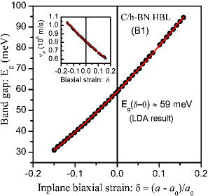
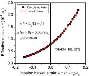
For C/h-BN HBL(B1), the calculated variation of (i) E
with in-plane homogeneous biaxial strain is depicted in
Figure 5, the inset shows the variation of with ; (ii)
with is depicted in Figure 6.
Our predicted strain-induced modifications of E, and
should affect the transport and optical properties of C/h-BN HBL, which may be probed
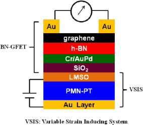
experimentally in a set-up (thought of as a specific amalgamation of the reported experimental [1, 2, 8] designs) like the one schematically shown in Figure 7.
Although further improvements in the design and materials of Figure 7 are
possible, the important message is that such an experiment is feasible with
the available technology as applied successfully in the experiments
[1, 2, 8]. In Figure 7, a simple h-BN back-gated BN-GFET[1, 2]
is rigidly fixed on a variable biaxial strain inducing system (VSIS) like
the one described in Ref. [8]. By applying a definite voltage across the VSIS,
a biaxial strain of definite magnitude can be induced in BN-GFET. The
current-voltage characteristics of the back-gated BN-GFET at different strain
conditions may be studied to see to what extent the biaxial strain affects
the transport properties of BN-GFET. Moreover, an optical probe of the direct
band-gap of C/h-BN HBL may be performed at different strained states of
BN-GFET in such a set-up. This opto-mechanical probe may ascertain if C/h-BN
HBL can be used in designing nano opto-mechanical systems (NOMS).
4 Conclusions
In conclusion, we have studied and compared the band structures of graphene and C/h-BN HBL (in biaxially strained and unstrained states) using density functional theory based FP-(L)APW+lo method. From the parallel slopes of the energy dispersion bands near K point of the BZ of these structures, we estimated identical values of Fermi velocity of the low energy charge carriers in them. From this and an estimated small value of effective mass , we infer the pristine graphene-like electronic properties of narrow-gapped C/h-BN HBL. However, these results do not necessarily reflect the measured transport properties of actual devices. In particular, the other important factors determining the actual device performance include the flatness of the substrate, surface phonon energy and scattering, and the trap charges as in the oxide substrates. The strain-induced modifications of the energy band gap, Fermi velocity and effective mass of charge carriers in C/h-BN HBL in its most stable configuration was studied in detail with output of some testable results for which a schematic experimental set-up has been proposed. The results, if verified, may find applications in future graphene-based NEMS, NOMS and other nano-devices.
References
- [1] I. Meric, C. Dean, A. Young, J. Hone, P. Kim, K.L. Shepard, Technical Digest International Electron Devices Meeting, IEDM, 2010, 23.2.1.
- [2] C.R. Dean, A.F. Young, I. Meric, C. Lee, L. Wang, S. Sorgenfrei, K. Watanabe, T. Taniguchi, P. Kim, K.L. Shepard, J. Hone, Nat. Nanotechnol. 5 (2010), 722.
- [3] A.K. Geim, Science 324 (2009) 1530.
- [4] A.H. Castro Neto, F. Guinea,N.M.R. Peres, K.S. Novoselov, A.K. Geim, Rev. Mod. Phys. 81 (2009) 109.
- [5] N.M.R. Peres, Rev. Mod. Phys. 82 (2010) 2673.
- [6] S.D. Sarma, E.H. Hwang, Phys. Rev. B 83 (2011)121405(R).
- [7] R.T. Weitz, A. Yacoby, Nat. Nanotechnol. 5 (2010) 699.
- [8] F. Ding, H. Ji, Y. Chen, A. Herklotz, K. Dörr, Y. Mei, A. Rastelli, O.G. Schmidt, Nano Lett. 10 (2010) 3453.
- [9] M. L. Lee, E.A. Fitzgerald, M.T. Bulsara, M.T. Currie, A. Lochtefeld, J. Appl. Phys. 97 (2005) 011101.
- [10] M. Chu, Y. Sun, U. Aghoram, S.E. Thompson, Annu. Rev. Mater. Res. 39 (2009) 293.
- [11] G. Giovannetti, P.A. Khomyakov, G. Brocks, P.J. Kelly, van den J. Brink, Phys. Rev. B 76 (2007) 073103.
- [12] J. Sławińska, I. Zasada, Z. Klusek, Phys. Rev. B. 81 (2010) 155433.
- [13] Y. Fan, M. Zhao, Z. Wang, X. Zhang, H. Zhang, Appl. Phys. Lett. 98 (2011) 083103.
- [14] J. Sławińska, I. Zasada, P. Kosiński, Z. Klusek, Phys. Rev. B 82 (2010) 085431.
- [15] A. Ramasubramaniam, D. Naveh, E. Towe, Nano Lett. 11 (2011) 1070.
- [16] J. Li, G. Gui, J. Zhong, J. Appl. Phys. 104 (2008) 094311.
- [17] R.M. Ribeiro, V.M. Pereira, N.M.R. Peres, P.R. Briddon, A.H. Castro Neto, New J. Phys. 11 (2010) 115002.
- [18] M. Farjam, H. Rafii-Tabar, Phys. Rev. B 80 (2009) 167401.
- [19] G. Gui, J. Li, J. Zhong, Phys. Rev. B 80 (2009) 167402.
- [20] Seon-M. Choi, Seung-H. Jhi, Young-W. Son, Phys. Rev. B 81 (2010) 081407(R).
- [21] Z.H. Ni, T. Yu, Y.H. Lu, Y.Y. Wang, Y.P. Feng, Z.X. Shen, ACS Nano 2 (2008) 2301.
- [22] T.M.G. Mohiuddin, A. Lombardo, R.R. Nair, A. Bonetti, G. Savini, R. Jalil, N. Bonini, D.M. Basko, C. Galiotis, N. Marzari, K.S. Novoselov, A.K. Geim, A.C. Ferrari, Phys. Rev. B 79 (2009) 205433.
- [23] M. Huang, H. Yan, T.F. Heinz, J. Hone, Nano Lett. 10 (2010) 4074.
- [24] O. Frank, M. Mohr, J. Maultzsch, C. Thomsen, I. Riaz, R. Jalil, K.S. Novoselov, G. Tsoukleri, J. Parthenios, K. Papagelis, L. Kavan, C. Galiotis, ACS Nano 5 (2011) 2231.
- [25] K.S. Kim, Y. Zhao, H. Jang, S.Y Lee, J.M. Kim, K.S. Kim, Jong-H. Ahn, P. Kim, Jae-Y. Choi, B.H. Hong, Nature 457 (2009) 706.
- [26] E. Sjöstedt, L. Nordström, D.J. Singh, Solid State Commun. 114 (2000) 15.
- [27] E. Wimmer, H. Krakauer, M. Weinert, J.A. Freeman, Phys. Rev. B 24 (1981) 864.
- [28] Elk is an open source code: http://elk.sourceforge.net/
- [29] J.P. Perdew, A. Zunger, Phys. Rev. B 23 (1981) 5048.
- [30] H. Behera, G. Mukhopadhyay, AIP Conf. Proc. 1313 (2010) 152.
- [31] H.J. Monkhorst, J.D. Pack, Phys. Rev. B 13 (1976) 5188.
- [32] F. Liu, P. Ming, J. Li, Phys. Rev. B 76 (2007) 064120.
- [33] E. Cadelano, P. L. Palla, S. Giordano, L. Colombo, Phys. Rev. Lett. 102 (2009) 235502.
- [34] X. Wei, B. Fragneaud, C. A. Marianetti, J. W. Kysar, Phys. Rev. B 80 (2009) 205407.
- [35] C. Lee, X. Wei, J. W. Kysar, J. Hone, Science 321(5887) (2008) 385.
- [36] G. Cocco, E. Cadelano, L. Colombo, Phys. Rev. B 81 (2010) 241412.
- [37] S. Wang, J. Phys. Soc. Jpn. 79 (2010) 064602.
- [38] K. Watanabe, T. Taniguchi, H. Kanda, Nat. Mater. 3 (2004) 404.
- [39] K.S. Novoselov, A.K. Geim, S.V. Morozov, D. Jiang, M.I. Katsnelson, I.V. Grigorieva, S.V. Dubonos, A.A. Firsov, Nature 438 (2005) 197.
- [40] E.V. Castro, N.M.R. Peres, J.M.B.L. dos Santos, F. Guinea, A.H. Castro Neto, J. Phys.: Conf. Ser. 129 (2008) 012002.