Aharonov-Bohm effect in an electron-hole graphene ring system
Abstract
Aharonov-Bohm oscillations are observed in a graphene quantum ring with a top gate covering one arm of the ring. As graphene is a gapless semiconductor this geometry allows to study not only the quantum interference of electrons with electrons or holes with holes but also the unique situation of quantum interference between electrons and holes. The period and amplitude of the observed Aharonov-Bohm oscillations are independent of the sign of the applied gate voltage showing the equivalence between unipolar and dipolar interference.
One of the best known effects that can be used
to observe and control quantum interference is the
Aharonov-Bohm (AB) effect AharonovBohmEffektFP1959[5] ; Exp4[9] .
During the last years the AB effect was intensively studied for two-dimensional systems in semiconducting
heterostructuresqdring1 ; qdring2 ; qdring3 . The introduction of graphene Erscheinungspaper2004[1]
opened new ways to study electronic and phase coherent transport in a two-dimensional system.
Therefore, several theoretical studies concerning the AB effect in graphene were
published in recent years Theorie2[11] ; Theory1[10] ,
but only very few experimental works were carried out Expr1[6] ; Exp2[7] ; Exp3[8] . One of the remarkable
effects in graphene is that both charge carrier types, electrons and holes,
can be induced in one and the same sample with local gates BandTheoryOfGraphite[2] ; TG4[17] ; TGsusp[18] . In such experiments new effects, like the rise of the
values of Quantum Hall plateaus TG(QHETHEORIE) ; Kleintunnelingtheorie[20]
and the non-perfect Klein tunneling Falko2006 ; Katsnelson2006 were observed.
In this paper we present an experiment where it is possible to combine the AB-effect
and Klein tunneling. While using a local gate to create a pnp-junction
we are able to show the AB-effect not only for an unipolar system
but also for an electron-hole system. Such interference between electrons and holes can only be observed due to our special sample structure and due to the unique bandstructure of graphene.
The sample was fabricated via a standard procedure: the graphene flake
was produced by mechanical exfoliation from natural graphite and
deposited on a thin layer of
on top of a heavily p-doped silicon wafer, which was used as a backgate (BG)
during the measurements. The sample was found to be a monolayer graphene
flake by optical microscopy using the light intensity contrast
shift analysis method in the green channel blake:063124 .
Electron beam lithography and oxygen plasma etching were used to define
a ring with an inner radius of and an outer radius of .
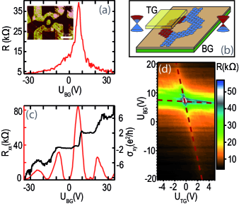
Figure 1 shows an image
of the etched device. In a second step Chromium/Gold contacts were evaporated.
In the third step another layer of Polymethylmethacrylate (PMMA) was
deposited on top of the flake to enable the fabrication of a topgate (TG)
using the PMMA as an insulator TG1[14] ; schmidt:Paper ; TG2[15] .
The Chromium/Gold topgate was evaporated over one arm of the ring (see Fig. 1(b)).
Before the measurements, the sample was annealed for more than eight
hours with an average temperature of to
reduce doping and increase mobility.
All measurements presented in this paper are four probe measurements and have been performed in a - cryostat with a base temperature of . A perpendicular magnetic field of up to was applied. The resistance was measured with a lock-in amplifier with a current of .
Figure 1(a) shows the measured resistance of the ring versus the backgate voltage. The charge neutrality point (CNP) is observed at a gate voltage of . We attribute this small but non-zero gate voltage to doping that has not been removed through the annealing process and to the extra layer of PMMA that was deposited on top of the sample. The sample was identified as monolayer graphene also by magnetotransport measurements which show the typical half integer Quantum Hall effect HIQHE_THEO ; QHE1[4] (see in Fig. 1(c)). The mobility for holes and for electrons was calculated from the backgate dependent resistance measurements, taking into account the geometric factor of the sample. The mean free path is approx. which is much smaller than the ring circumference . This means that the measured system is in the diffusive regime.
Such transport measurements are also used to characterize the topgate coupling. Figure 1(d) shows the colour intensity plot of the ring resistance as a function of backgate and topgate voltage. One can clearly see both CNPs (indicated by dashed red lines), which divide the color plot in four different regions: two unipolar (electrons-electrons, holes-holes) and two bipolar regions (electrons-holes, holes-electrons). The coupling factor is in good agreement with the expected parallel capacity coupling model based on the distance of between flake and topgate.
Figure 2 shows the AB effect measurements for a fixed backgate voltage and vanishing topgate voltage corresponding to . The magnetic field was swept in a limited range around zero magnetic field in order to avoid the occurrence of Shubnikov-de Haas oscillations. Figure 2(a) shows the ring resistance as a function of magnetic field. A peak can be observed at zero Tesla which is attributed to weak localization. Small oscillations are seen over the whole shown magnetic-field range. These oscillations have an average visibility of and can be identified as AB oscillations. Figure 2(b) shows the AB oscillations with the background subtracted. The background resistance was obtained by a running average over a number of AB periods with a minimum of one period Expr1[6] ; Exp2[7] .
Figure 2(c) shows the Fourier spectrum of the oscillations presented in Fig. 2(b). The Fourier spectrum has a peak at which corresponds to a period of . The expected period for a ring with an average radius of is , so the measured oscillations match the first harmonic and fit the size of the ring. The black curve is a Gaussian fitted to the Fourier spectrum. The curve illustrates the period of the oscillations and the spreading which can be a hint towards the different paths possible within the geometric width of the ring. In the Fourier spectrum we observe a tail around , which can be an indication towards the second harmonic and explains the strong modulation of the oscillations. The phase coherence length of our system has to be shorter than two times the ring circumference, since there appear only indications of a second harmonic.
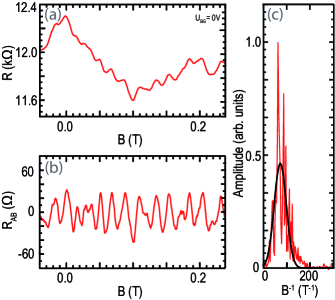
AB measurements are reported with comparable results in Refs. Exp2[7] ; Exp3[8] ; Expr1[6] . For comparison in Ref. Expr1[6] oscillations were measured with a visibility of less than 1% in low magnetic fields which was attributed to a possible defect in one arm of the ring. Other experiments showed AB oscillations with a visibility of up to 5% for a sample with a side gate Exp2[7] . In both experiments no second harmonics oscillations were observed in low magnetic fields. Our observed visibility is comparable with the results presented in Expr1[6] but we cannot connect the results with a defect in our sample.
In contrast to the previous experiments, our experimental set-up allows the generation of different charge carriers in the two arms of the ring by varying the topgate voltage. The topgate-dependent measurements are performed as follows: Firstly the backgate voltage was fixed at a certain value to define the carrier type and the concentration in the leads and one arm of the ring. Secondly the topgate voltage was set to define the charge carriers in the second arm of the ring. Thirdly the magnetic field was swept and the voltage was measured and the resistance calculated. The AB oscillations were obtained by subtracting the background resistance as described before and the absolute amplitude of the resulting oscillations are analyzed by the root mean square (RMS) value.
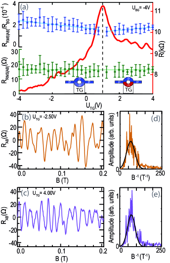
A typical measurement is presented in Fig. 3(a). It shows the resistance of the ring versus the topgate voltage with a fixed backgate voltage (red line), so that one side of the ring and the leads have holes as charge carriers with a concentration of due to the fixed backgate voltage, whereas the other side of the ring has a different charge concentration due to the influence of the topgate voltage. The resistance of the topgate dependent CNP at with is much lower in comparison to the backgate dependent CNP (Fig. 1(a)) with approx. . This behavior is attributed to the small topgate-covered area which is only one arm of the ring and is essentially smaller than the sum of the other arm and the leads of the sample.
The CNP divides the graph into two regions with different charge carriers in the second arm of the ring: holes on the left and electrons on the right side. The asymmetry of the resistance is based on the non-perfect Klein tunneling which depends strongly on the smoothness of the potential step Falko2006 ; Katsnelson2006 . The higher resistance on the right side of the graph shows the existence of the pnp junction created in one arm of the ring. So Fig. 3(a) presents an unipolar system on the left and a bipolar system on the right side of the CNP.
Whereas there is no clear observation of the AB oscillations at the CNP, oscillations are observed away from the CNP.
Two sets of oscillations with a subtracted background are shown in Fig. 3(b) (unipolar) and 3(c) (dipolar). The charge carrier concentrations used in these two measurements are of similar magnitude but different polarity. In both situations the absolute amplitude is quite similar. The period of the oscillations is also not affected by the unipolar or dipolar situation as seen from the Fourier spectra shown in Fig. 3(d) and 3(e). The AB oscillations were analyzed for a number of different topgate voltages. The RMS values of the absolute amplitude is analyzed as described before and plotted versus the topgate voltage in Fig. 3(a) as green dots. The measured RMS of the absolute amplitude is more or less constant with an average value of as indicated in Fig. 3(a) by the horizontal green line. It does not change for different charge carrier type and concentrations. The period of the oscillations is observed to be also constant in these topgate dependent measurements.
The relative amplitude is the absolute amplitude divided by the mean of the background resistance and can be used to characterize the visibility of the oscillations. The relative amplitudes are shown as blue dots versus the topgate voltage in Fig. 3(a) for our measurements. One observes a linear decrease towards the topgate dependent CNP in both regions due to the overall increase in resistance. The absolute value of the slope is higher in the unipolar region than in the bipolar by a factor of . The minimum visibility in these measurements is approx. 0.2% while the maximum visibility reaches 0.3%. This behavior is caused by the asymmetry of the overall resistance while the actual absolute amplitude of the oscillations being almost constant in both regions. In Ref. TheorieKleintunneling[13] the difference in visibility for the unipolar and bipolar situation was explained by the tunneling of the charge carriers through the junction and their interference with themselves. The resulting difference in the relative amplitude is observed in our experiment, but the astonishing fact remains that the absolute amplitude of the observed oscillations is independent of whether holes interfere with holes or electrons interfere with holes.
In conclusion we have reported AB oscillations in a monolayer graphene ring with a period that fits the geometry of the ring. Our measurements show that AB oscillations are possible in a ring system with a pnp junction. No changes of period or amplitude are observed for this dipolar regime.
We acknowledge discussions with P. Recher. This work was supported
by the DFG via SPP 1459, the excellence cluster QUEST and the NTH
School for Contacts in Nanosystems.
References
- (1)
- (2) Y. Aharonov and D. Bohm, Phys. Rev. 115, 485, 1959.
- (3) R. A. Webb, S. Washburn, C. P. Umbach, and R. B. Laibowitz, Phys. Rev. Lett. 54, 2696, 1985.
- (4) R. Schuster, E. Buks, M. Heiblum, D. Mahalu, V. Umansky, and H. Shtrikman, Nature 385, 417, 1997.
- (5) A. Fuhrer, S. Lüscher, T. Ihn, T. Heinzel, K. Ensslin, W. Wegscheider, and M. Bichler, Nature 413, 822, 2001.
- (6) U. F. Keyser, C. Fühner, S. Borck, R. J. Haug, M. Bichler, G. Abstreiter, and W. Wegscheider, Phys. Rev. Lett. 90, 196601, 2003.
- (7) K. S. Novesolelov, A. K. Geim, S. V. Morozov, D. Jiang, Y. Zhang, S. V. Dubonos, I. V. Grigorieva, and A. A. Firsov, Science 306, 666, 2004.
- (8) R. Jackiw, A. I. Milstein, S. Y. Pi, and I. S. Terekhov, Phys. Rev. B 80, 033413, 2009.
- (9) P. Recher, B. Trauzettel, A. Rycerz, Ya. M. Blanter, C. W. J. Beenakker, and A. F. Morpurgo, Phys. Rev. B 76, 235404, 2007.
- (10) S. Russo, J. B. Oostinga, D. Wehenkel, H. B. Heersche, S. S. Sobhani, L. M. K. Vandersypen, and A. F. Morpurgo, Phys. Rev. B 77, 085413, 2008.
- (11) M. Huefner, F. Molitor, A. Jacobsen, A. Pioda, C. Stampfer, K. Ensslin, and T. Ihn, New Journal of Physic 12, 043054, 2010.
- (12) J. S. Yoo, Y. W. Park, V. Skakalova, and S. Roth, Appl. Phys. Lett. 96, 143112, 2010.
- (13) P. R. Wallace, Phys. Rev. 71, 622-634, 1947.
- (14) B. Özyilmaz, P. Jarillo-Herrero, D. Efetov, D. A. Abanin, L. S. Levitov, and P. Kim, Phys. Rev. Lett. 99, 166804, 2007.
- (15) G. Liu, J. Velasco Jr., W. Bao, and C. N. Lau, Appl. Phys. Lett. 92, 203103, 2008.
- (16) D. A. Abanin, and L. S. Levitov, Science 317, 641, 2007.
- (17) J. R. Williams, L. DiCarlo, and C. M. Marcus, Science 317, 638, 2007.
- (18) V. V. Cheianov, and V. I. Fal’ko Phys. Rev. B. 74, 041403, 2006.
- (19) M. I. Katsnelson, K. S. Novoselov and A. K. Geim, Nat Phys 2, 620, 2006.
- (20) P. Blake, E. W. Hill, A. H. Castro Neto, K. S. Novoselov, D. Jiang, R. Yang, T. J. Booth, and A. K.Geim, Appl. Phys. Lett. 91, 063124, 2007.
- (21) B. Huard, J. A.Sulpizio, N. A.Stander, K. Todd, B.Yang, and D. Goldhaber-Gordon, Phys. Rev. Lett. 98, 236803, 2007.
- (22) H. Schmidt, T. Lüdtke, P. Barthold, E. McCann, V. I. Fal’ko, and R. J. Haug, Appl. Phys. Lett. 93, 172108, 2008.
- (23) T. Lüdtke, H. Schmidt, P. Barthold, and R. J. Haug, Physica E 42, 695, 2010.
- (24) V. P Gusynin and S. G. Sharapov, Phys. Rev. Lett. 95, 146801, 2005.
- (25) K. S. Novoselov, A. K. Geim, S. V. Morozov, D. Jiang, M. I. Katsnelson, I. V. Grigorieva, S. V. Dubonos, and A. A. Firsov, Nature 438, 197, 2005.
- (26) J. Schelter, D. Bohr, and B. Trauzettel, Phys. Rev. B 81, 195441, 2010.