Mechanical annealing of metallic electrodes at the atomic scale
Abstract
The process of creating an atomically defined and robust metallic tip is described and quantified using measurements of contact conductance between gold electrodes and numerical simulations. Our experiments show how the same conductance behavior can be obtained for hundreds of cycles of formation and rupture of the nanocontact by limiting the indentation depth between the two electrodes up to a conductance value of approximately in the case of gold. This phenomenon is rationalized using molecular dynamics simulations together with density functional theory transport calculations which show how, after repeated indentations (mechanical annealing), the two metallic electrodes are shaped into tips of reproducible structure. These results provide a crucial insight into fundamental aspects relevant to nano-tribology or scanning probe microscopies.
pacs:
62.25.-g, 73.63.Rt, 73.22.-fAn important source of uncertainty in electrical measurements at the atomic scale is rooted in the indefinite structure of the metallic electrodes, regardless of whether they are created by mechanical, electrical, or electrochemical meansTsong90 ; Mel90 . Many technological applications and fundamental studies would benefit from atomically defined, stable, and reproducible metallic electrodes down to the nanoscale. For example, often before a measurement using scanning tunnelling microscopy (STM), the tip has to be prepared by indenting several times on a surface until a clear image can be obtained. To date, despite the importance of this process, there is no rigorous study or quantification of the underlying physical mechanisms.
The formation of atomic scale contacts between two metallic systems is usually performed by STM AgrRod93 ; PasMen93 or by mechanically controlled break junctions (MCBJ) MulRui92 . The evolution of the minimum cross section of these contacts can be followed by recording traces of conductance while the electrodes are displaced with respect to each other. Generally, the conductance traces obtained differ between different experimental runs and a statistical approach is used, recording conductance histograms in order to identify preferential configurations OleLag95 ; KraRui95 . This phenomenon has been extensively studied both experimentally and theoretically AgrLev03 .
There are, however, certain situations where the same conductance traces are recurrent during hundreds of cycles of compression or traction. It was shown UntRub97 that when a 100 atom thick contact is properly trained through repeated indentation, it is possible to improve its crystallinity and aspect-ratio as long as the wire is not broken during this process. In the opposite limit, Trouwborts et al TroHui08 showed that they could form stable one-atom contacts by gently cycling the formation of a one-atom contact from rupture. These results have been recently modelled through molecular dynamics simulations Wang11 .
In this paper we present, using both experiments and simulations, a comprehensive study of the formation process of an atomically defined stable gold tip through repeated indentations. Experiments allow us to quantify the indentation values for the formation of a robust tip, while electronic and atomic structure simulations provide an explanation to this fact. Remarkably, we show that reproducible traces can be obtained even when the tips are indented up to a conductance of , where plastic deformation was expected to occur. The results presented here shed light on the process of preparation of STM tips and, in general, on the formation of stable and reproducible metallic electrodes.
To produce atomic contacts we have used a low temperature STM where tip and sample consist of two gold electrodes of purity above 99.995% . Prior to the experiments the samples are carefully cleaned in an acetone bath. All experiments are performed at low temperatures (4.2K) under a cryogenic vacuum atmosphere, to ensure cleanness. Applying a constant bias voltage of to the junction the electronic current is measured while displacing the two electrodes with respect each other. In this way, conductance vs. electrode displacement is constructed during the formation and rupture of the contact, reflecting its structural evolution. We have done a systematic study of the evolution and reproducibility of these traces, comparing their behaviour for different values of the maximum conductance during indentation, .
Figure 1(a) shows 286 consecutive conductance traces during the formation and rupture of gold nanocontacts when we limit the maximum value of conductance to . The inset shows a three dimensional graph of the rupture cases. One can clearly observe that the traces remain unchanged during hundreds of cycles with most of them showing the same height and length for the different steps. This is a remarkable result considering that these conductance values correspond to cross sections of a few atoms where one would expect plastical deformation to occur. In Figure 1(b) the conductance traces for formation and rupture of the gold contact are shown when the maximum conductance is limited to a value of . The inset figure shows the three dimensional plot of the same traces. The difference between the traces in Fig. 1(a) and (b) are outstanding: for the larger indentation the traces are not reproduced for consecutive cycles.
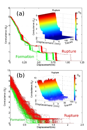
Two major conclusions can be drawn from these experimental results. On one hand, if one is interested in obtaining a representative histogram of the conductance behavior of a particular metal, exploring many different configurations, it is important to indent the two electrodes to values higher than a threshold conductance ( in the case of gold). Otherwise, one might end up in a stable configuration that will bias the statistical result. On the other hand, these results also show a quantitative way to obtain a robust STM tip or electrode: one must indent the tip several times to a conductance value not higher than a given threshold value. The values of conductance provided here are for the case of gold, but experiments in other materials are currently being performed.
These experiments, however, do not provide atomic scale information or the mechanism that gives rise to this behaviour. Numerical simulations are now used in order to gain some understanding and provide an explanation consistent with the experimental results. Molecular dynamics (MD) with empirical potentials is the computational tool most commonly used to study the breaking and formation process of a nanocontact Landman ; Sorensen98 ; HasMed01 ; GarPel05 ; Palacios05 ; DreHeu04 ; PauDre06 ; CalCat08 . The conductance is expected to be proportional to the minimum cross section of the contact in an MD simulation. Therefore, histograms of minimum cross sections can be correlated, more or less accurately, with conductance histograms. Usually this correlation is better done through other computational methods such as density functional theory (DFT) Palacios05 or tight-binding DreHeu04 ; PauDre06 electronic transport calculations. In these MD simulations different traces are obtained varying slightly the initial conditions, generally changing the initial velocity distributions, but using the same initial geometry.
We have performed MD simulations of breaking and formation of gold nanocontacts using the embedded atom potential developed by Zou et al. PotentialGold . This potential is fitted to reproduce basic materials properties such as lattice constant, elastic constant, bulk moduli, and vacancy formation energy. The initial configuration is a neck, following the work of Sorensen et al Sorensen98 . The ratio between the length of the neck and the narrowest cross section is 5 for simulations with 525 atoms and 2 for simulations with 2804 atoms. In this way we mimic a long and narrow nanowire and a short and wide constriction. Three atomic layers at the top and at the bottom of the simulation cell are displaced by a fixed distance ( every time step, with characteristic strain rates between and Sorensen98 . The temperature in the simulations is controlled in two different ways: it is kept constant by scaling the velocities of all atoms every time step (every femtosecond) as done in other works HasMed01 ; GarPel05 ; PauDre06 , or the temperature is not fixed during the calculation but it is scaled in every cycle, after the contact is broken. In this last case the maximum raise in temperature is 70K. The initial temperature for both cases is 4.2 K. Unlike previous works HasMed01 ; GarPel05 ; DreHeu04 ; PauDre06 ; CalCat08 , calculations are performed in cycles, following the experimental procedure. A tension along the direction is applied to the initial structure until it breaks. Computing the minimum cross section Brat of the nanocontact while stretching allows us to identify when then contact is broken. Once the contact is broken, the system is allowed to evolve during another 200 steps to ensure that the two tips are well separated. Then the two tips are brought in contact again (by applying a compression) until a given cross section (which has varied) is reached. This cycle is repeated at least 20 times for each case.
Figure 2, top section, shows 6 snapshots of the nanocontact during the formation and breaking process for the case of the narrow nanowire. The results presented are the initial configuration and the configuration of the system before cycles 2, 5, 10, 15 and 20. In this particular calculation the temperature was not kept fixed and the two nanoelectrodes are brought together until the minimum cross section reaches a size of 15 atoms. The atoms have been colored according to the following procedure: after the nanocontact is broken for the first time, atoms in the top nanoelectrode and in the bottom one are labeled differently, as shown in the configuration for cycle 2. Therefore, the number of atoms that are exchanged between electrodes, with respect to the original configuration, can be followed (see cycles 5 to 20). Figure 2 shows the percentage of atoms on one nanoelectrode that were originally on the second one, for the two nanoelectrodes, as a function of the indentation cycle. The figure shows how this number reaches a constant value after 7 - 8 cycles. Note that during the second cycle the nanocontact breaks from a different point leaving only one nanoelectrode with mixed atoms. This can be seen more clearly in the movie of the complete calculation Movie1 .
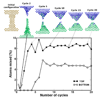
The first interesting feature that can be observed from the different configurations in Figure 2 is the re-shaping of the two sides with the indentation cycles. The second cycle shows the formation of long chains, in this case a double chain, which have been already identified and described by other authors Double_ch . However, as the indentation process continues, stable tips are formed which remain almost unchanged for cycles 10, 15 and 20. The constant value in the atomic mixing between tips for these cycles also points to the formation of a stable configuration. The tips formed have a pyramidal shape with faces, which is consistent with energetic considerations.
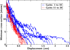
The formation of a robust tip after repeated indentations can also be observed in the traces of the minimum cross section (in number of atoms) obtained from the simulations. In figure 3 traces for all 20 indentations for the case of stretching the nanocontact until rupture are presented. It is clear from this figure that while the first 10 traces are very different from each other, the last 20 traces are quite similar, just like the experimental data shown in Fig. 1.
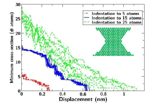
The reproducibility of the traces in the simulations depends, at least, on two factors. On one hand, if the temperature is kept fixed in the simulations as done in previous calculations Sorensen98 ; HasMed01 , traces are much more similar to each other than if no heat dissipation is included. However, there is also less relaxation of the atoms in the two tips and that results, in some cases, in the formation of unlikely structures. Note that keeping the temperature fixed is equivalent to an almost instant dissipation of heat (femtoseconds). A second factor that influences the reproducibility of the traces is the initial atomic configuration. When the initial structure is a short and wide constriction, the two pyramidal tips are easily formed after the first indentation and all subsequent traces are very similar as long as the maximum indentation value is kept low. Figure 4 shows the minimum cross section for the case of 2804 atoms, with fixed temperature and for three different indentation values: cross section of 5, 15 and 25 atoms. The inset in this figure shows the initial configuration in this simulation. This result clearly shows that if the indentation is kept low, below a minimum cross section of 15 atoms, the traces are nicely reproduced, just like in the experiments shown in Fig. 1(a). However, when the indentation is up to a section of 25 atoms, the traces are very different from one cycle to the next, even in the case where heat is dissipated. This is also in agreement with the experimental data shown in figure 1(b). This behavior is the result of the sliding between the two tips. For small indentations the tips can accomodate each other by simply sliding along the faces with almost no disorder of any of the two tips. However, as the indentation proceeds disorder of the tips increases, changing their shapes and consequently the traces obtained (see movies2and3 for movies of these calculations.
MD simulations, however, do not provide precise information about conductance of these systems and therefore cannot be directly compared with the experimental measurements. For the case of gold, which has a single valence orbital half occupied, one could use a simple rule of thumb and consider that the cross section in atoms is equal to the conductance in units of . However, this might not be the case when the minimum cross section has several atoms and the lattice is disordered. Therefore, we have performed DFT electronic transport calculations to obtain the conductance values for the atomic configurations obtained with the MD simulations. We have used our code ANT.G, which is part of the package ALACANT ALACANT and implements the non-equilibrium Green’s function formalism with the help of the popular code GAUSSIAN09 GAUSSIAN09 .
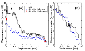
Figure 5 shows two conductance traces for the first and tenth ruptures along with the minimum cross section for the case of the narrow wire (525 atoms). Here, due to the large number of atoms, we have employed a very basic basis set consisting only of one orbital and one electron, the remaining 78 electrons being part of the pseudopotential. For reassurance, we have also computed a few MD snapshots with a larger basis set consisting of orbitals and 11 electrons (diamonds, in figure 5(a)). These calculations show that for small cross sections, up to , there is an equivalence between conductance and number of atoms in the minimum cross section. However, for larger cross sections this correspondence does no longer holds, which can be attributed, in part, to the disordered structure. In this particular case the conductance of a cross section with atoms is reduced to only . This could explain why in the molecular dynamics simulations described above we obtain stable traces for indentation up to cross sections of atoms, while experimentally the indentation must be limited to .
In summary, our experiments show that it is possible to create stable and atomically well-defined tips by repeated indentation of an electrode into a surface as long as the indentation is limited to a few conductance quanta: in the case of gold. Our simulations show how, under repeated indentations, two pyramidal tips with faces form. When the indentation is small, the tips will slide on each other producing almost no distortion and, therefore, reproducible traces. As the indentation increases so does the disorder and the reproducibility disappears.
This work was supported by the Spanish government through grants FIS2010-21883 and CONSOLIDER CSD2007-0010.
References
- (1) T.T. Tsong. Atom-Probe Field Ion Microscopy. Cambridge University Press, (1990)
- (2) A.J. Melmed, J. Vac. Sci. Technol. B 9 601(1991)
- (3) N. Agrait, J.G. Rodrigo, and S. Vieira, Phys. Rev. B 47, 12 345 (1993)
- (4) J.I. Pascual, J. Mendez, J. Gomez-Herrero, A.M. Baro, and N. Garcia, Phys. Rev. Lett. 71, 1852 (1993)
- (5) C.J. Muller, J.M. van Ruitenbeek, and L.J. de John, Physica C 191, 485 (1992)
- (6) L. Olesen,E. Lagsgaard, I. Stensgaard, F. Besenbacher, J. Schiotz, P. Stoltze, K. W. Jacobsen, J. K. Norskov, Phys. Rev. Lett. 74, 2147 (1995)
- (7) J. M. Krans, J. M. van Ruitenbeek, V. V. Fisun, I. K. Yanson, L. J. de Jongh, Nature 375, 767 (1995)
- (8) N. Agrait, A. Levy-Yeyati, J. M. van Ruitenbeek, Phys. Rep. 377, 81 (2003)
- (9) C. Untiedt, G. Rubio, S. Vieira and N. Agrait, Phys. Rev. B 56, 2154 (1997)
- (10) M. L. Trouwborst, E. H. Huisman, F. L. Bakker, S. J. van der Molen and B. J. van Wees1, Phys. Rev. Lett. 100, 175502 (2008)
- (11) H. Wang and Y. Leng, Phys. Rev. B 84, 245422 (2011)
- (12) U. Landman, W. D. Luedtke, N. A. Burnham and R. J. Colton, Science 248, 454 (1990).
- (13) M. R. Sorensen, M. Brandbyge, and K.W. Jacobsen, Phys. Rev. B 57, 3283 (1998)
- (14) A. Hasmy, E. Medina, P. Serena, Phys. Rev. Lett. 86, 5574 (2001)
- (15) P. Garcia-Mochales, X. Pelaez, P. A. Serena, E. Medina, A. Hasmy, Appl. Phys. A-Materials Science and Processing 81, 1545 (2005)
- (16) A. Hasmy, A. J. Pérez-Jiménez, J. J. Palacios, P. García-Mochales, J. L. Costa-Krämer, M. Díaz, E. Medina, and P. A. Serena, Phys. Rev. B 72, 245405 (2005).
- (17) M. Dreher, F. Pauly, J. Heurich, J. C. Cuevas, E. Scheer, P. Nielaba, Phys. Rev. B 72, 075435 (2005)
- (18) F. Pauly, M. Dreher, J.K. Viljas, M. Hafer, J.C. Cuevas, P. Nielaba, Phys. Rev. B 74, 235106 (2006)
- (19) A. R. Calvo, M. J. Caturla, D. Jacob, C. Untiedt, J. J. Palacios, IEEE TRANSACTIONS ON NANOTECHNOLOGY 7, 165 (2008)
- (20) Zhou et al, Act. Met. 49, 4005 (2001).
- (21) A. M. Bratkovsky et al., Phys. Rev. B 52 5036 (1995)
- (22) Movie for 525 atoms and indentation up to 15 atoms (Movie1).
- (23) H. Ohnishi, Y. Kondo, and K. Takayanagi, Nature, 395, 780 (1998).
- (24) Movies for 2804 atoms and indentation up to 25 atoms (Movie2) and 15 atoms (Movie3).
- (25) ALicante Atomistic Computation Applied to NanoTransport. Package publicly available at http://alacant.dfa.ua.es.
- (26) M. J. Frisch et al., Gaussian 09 revision a.1, Gaussian Inc. Wallingford CT 2009.