Molecular-beam epitaxial growth of a far-infrared transparent electrode for extrinsic Germanium photoconductors
Abstract
We have evaluated the optical and electrical properties of a far-infrared (IR) transparent electrode for extrinsic germanium (Ge) photoconductors at 4 K, which was fabricated by molecular beam epitaxy (MBE). As a far-IR transparent electrode, an aluminum (Al)-doped Ge layer is formed at well-optimized doping concentration and layer thickness in terms of the three requirements: high far-IR transmittance, low resistivity, and excellent ohmic contact. The Al-doped Ge layer has the far-IR transmittance of % within the wavelength range of 40–200 m, while low resistivity (5 cm) and ohmic contact are ensured at 4 K. We demonstrate the applicability of the MBE technology in fabricating the far-IR transparent electrode satisfying the above requirements.
1 Introduction
Bulk germanium extrinsic photoconductors (Ge PCs) have been widely used in far-infrared (far-IR) astronomical observations in the 50–120 m wavelength range (e.g. Haegel et al., 1985). The spectral response of p-type Ge PCs can be extended to longer wavelengths (200 m) by applying a uniaxial compressive stress (Kazanskii et al., 1977). In order to provide high quantum efficiency, broad spectral response, and low cosmic-ray hitting rates compared to those for the bulk Ge PCs, germanium blocked impurity band (Ge BIB) detectors have been developed as next-generation far-IR detectors replacing the bulk Ge PCs (Watson & Huffman, 1988; Wu et al., 1991; Watson et al., 1993; Huffman & Casey, 1993; Bandaru et al., 2002; Beeman et al., 2007; Kaneda et al., 2011).
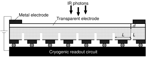
BIB detectors require electrodes with not a transverse but a longitudinal, and thus transparent configuration to obtain high responsivity, because a far-IR absorbing thin layer ( m) is formed underneath an electrode. And, the construction of a large-format array for both PCs and BIB detectors is indispensable to improve observational efficiency and measurement accuracy. The array as shown in Fig. 1 also needs electrodes with the far-IR transparent configuration. Although such transparent electrodes have been applied to Ge PC arrays, performance of transparent electrodes is not optimized (eg. Fujiwara et al., 2003).
The transparent electrode requires high far-IR transmittance, while it must ensure high conductivity and an excellent ohmic contact at temperatures below 4 K. To obtain high far-IR transmittance, a thin layer with a low doping concentration is desirable. On the other hand, a low resistivity layer equipped with excellent ohmic contact can be achieved by a degenerately doped (– cm-3), thick, and epitaxially grown Ge layer. Thus, the doped Ge layer should be epitaxially grown with optimally-controlled doping concentration and thickness.
Most commonly used technique to fabricate the transparent electrode is ion implantation on one surface of a device. However, its doping concentration often shows a graded profile. Therefore, the formation of the decreasingly-doped layer as a function of implant depth is inevitable. Such a broad doping profile significantly degrades far-IR transmittance due to photon absorption within the thick-implanted layer by free carriers and doped impurities (Hadek et al., 1985; Fujiwara, 2000). Nevertheless, there are few investigations in terms of abruptness for the doping profile.
To improve far-IR transmittance, an alternative process technology with precise control of a doping profile, a doping concentration and a layer thickness should be introduced. A promising candidate technology is molecular beam epitaxy (MBE) that is an Ultra-High-Vacuum (UHV)-based technique for producing high quality epitaxial structures with monomolecular layer (monolayer) thickness control. MBE technology allows us to accurately control doping profiles, doping concentrations, and interfaces, thanks to the lower growth rate and temperature compared to other epitaxial growth technologies such as liquid phase epitaxy. In this paper, we show the properties of the far-IR transparent electrode fabricated by the MBE technology.
2 Requirements for a far-IR transparent contact
In this section, we search optimized solutions for the doping concentration and the layer thickness , considering the following requirements: high far-IR transmittance, low resistivity, and excellent ohmic contact. Note that we assume all the dopants are electrically activated; , where is activated doping concentration.
2.1 Far-IR transmittance
The far-IR transmittance through a sample is defined as , where and are intensities of incident and transmitted far-IR light, respectively. We consider two samples; Sample-1 is a non-doped Ge wafer with a doped Ge layer, while Sample-2 is a non-doped Ge wafer without a doped Ge layer. Hereafter, we call the relative transmittance between the two samples as the far-IR transmittance of the doped Ge layer .
We require at K and m. To calculate , we take into account the free-carrier absorption and photoionization processes in the doped Ge layer with multiple refraction at the doped layer based on Hadek et al. (1985). They presented a theoretical analysis of the far-IR transmittance through ion-implanted Ge samples taking into account free-carrier absorption in the doped Ge layer with its impurity concentration range of cm-3. In their analysis, they introduced an absorption parameter in the Fresnel coefficients to calculate the transmittance from the vacuum to the non-doped Ge medium through the doped Ge layer and the reflectance from the doped Ge layer surface (see Fig. 4 of Hadek et al., 1985). In our calculation, to include the photoionization process, the absorption parameter is redefined as , where , , and are a photoabsorption coefficient, the complex refractive index of Ge, and the speed of light, respectively; Hadek et al. (1985) case corresponds to the case of . The photoabsorption coefficient is , where is a photoionization cross-section of a dopant. The complex refractive index depends on the infrared conductivity = , where and are the dc conductivity and a single relaxation time, respectively (Hadek et al., 1985).
The layer thickness and doping concentration at =0.95 are calculated by considering the DC conductivity dependence on impurity concentration at 4 K in Hadek et al. (1985) and assumed to be 10-14 cm-2 (Bratt, 1977; Wang et al., 1986). As a result, as can be seen in Fig. 2, smaller thickness and lower doping concentration than those on the solid line are required to achieve .
2.2 Resistivity
The requirement for the resistivity is that the resistance of the doped Ge layer () is much lower than that of a Ge PC pixel () for a voltage drop to become negligible at the layer. The requirement is particularly stringent for the large-format array to uniformly apply a detector bias voltage to pixels. Here, we consider an -pixel array that has the same electrode configuration as that in Fig. 1; the array has a common doped Ge layer for the pixels. A common metal electrode is formed on the doped Ge layer of pixels on the outermost circumferential sides. At the central pixel of the array, which is farthest from the metal electrode, the fraction of the bias voltage drop is expressed as . To obtain , the resistivity of the doped Ge layer at 4 K should be , where and are the resistivity of the Ge PC pixel at 4 K and the pixel size, respectively. The experimental relation between and is obtained from Fritzsche & Cuevas (1960). The dashed line in Fig. 2 is derived from the above equation on condition that , , and are cm (Hiromoto et al., 1989), cm, and 128, respectively.
2.3 Ohmic contact
To make an ohmic contact, a contact resistance needs to be sufficiently small compared with . Sze & Ng (2007) introduced the characteristic energy to categorize a carrier transport process for metal-semiconductor contacts. For p-type Ge with doping concentration of cm-3, is estimated to be eV by applying the hole effective mass of 0.075 (Hadek et al., 1985). Under the operation temperature ( K) of Ge PCs, is much higher than , which means a pure tunneling process through a Schottky barrier dominates. In this process, higher doping concentration is required. Also, the thickness of the doped Ge layer should be larger than that of the depletion width due to the metal/Ge contact.
As a typical pixel of Ge PCs, is estimated to be by using and at 4 K. Under the tunneling process, the specific contact resistance () depends strongly on , the carrier effective mass (), and the barrier height (), but virtually independent of temperature (Sze & Ng, 2007). Based on for a metal/n-type Ge contact measured by Gallacher et al. (2012) ( cm2 for cm-3 and eV), by applying effective masses of hole and electron (0.2 , Kahn, 1955), we roughly estimate for a metal/p-type Ge contact as
| (1) |
For an Al/Ge contact, since is 0.5 eV at 4 K (Thanailakis & Northrop, 1973; Sze & Ng, 2007), is estimated to be cm2 for cm-3. Therefore, we obtain by dividing by , which is much lower than ; the condition of is satisfied for cm-3.
In the case of , which means a voltage drop at the contact is negligible, is simply expressed as , where and (0.5 V at 4 K) are the permittivity of Ge and built-in voltage, respectively. In Fig. 2, the dash-dotted line corresponds to the condition of for the Al/Ge contact.
From the above three requirements, the enclosed area by the three lines in Fig. 2 shows optimized solutions for the fabrication of the far-IR transparent electrode for Ge PCs.
3 Experiments
3.1 Molecular beam epitaxial growth
Our MBE system is built inside a growth chamber, and contains effusion cells for source materials, a substrate holder and heater, a pumping system to achieve UHV (– Torr), liquid N2 cyropanels, and in-situ analysis tools: a reflection high energy electron diffraction (RHEED) gun and a mass spectrometer. A RHEED pattern on a screen and its brightness are measured by a CCD camera.
The source Ge was prepared from a non-doped Ge ingot with a resistivity of 49–51 cm, which means that its impurity concentration is much less than the room-temperature intrinsic carrier concentration in Ge ( cm-3). As for a dopant, since the non-doped Ge shows a p-type conduction below K by Hall effect measurements, the dopant is selected from p-type materials for Ge; we chose aluminum (Al, 6N purity). Crucibles for Ge and Al are pyrolytic boron nitride (PBN). The effusion cell temperature for Ge is set to be 1250 °C at which we observe the Ge beam flux of cm-2 sec-1. Since the fraction of electrical activation of Al in Ge is % for our MBE system (), the target Al doping concentration is 4–5 cm-3 to give wider acceptable range in thickness (see Fig. 2). The effusion cell temperature for Al is set to be 690 °C, which corresponds to the Al beam flux of cm-2 sec-1.
We prepared a mirror-polished Ge(100) substrate ( mm2) with thickness of 300 m, which was obtained from the non-doped Ge ingot. The substrate was degreased in methanol with ultrasonic for 10 min. After degreasing, the substrate was ultrasonically rinsed in deionized water (18 M cm) for 10 min to dissolve the native Ge oxide and then (I) dipped into HF (49 % HF:H2O =1:3) solution for 10 min. After the process, (II) the substrate was blown dry in dry N2 and then exposed to 8 mW cm-2 of radiation from a UV Hg arc lamp ( nm) in air for 10 min to remove carbon (C) atoms and grow a fresh Ge oxide layer. Then we repeated processes (I) and (II) but with duration time of 70 min with UV irradiation. The cleaned substrate was immediately introduced through a load lock into a UHV chamber. Prior to MBE growth, we checked carbon coverage of the substrate surface by X-ray photoelectron spectroscopy (XPS) analysis. By measuring intensities of Ge3d and C1s XPS lines, carbon coverage is estimated to be 0.08 monolayers that corresponds to the value for the HF treatment method in Sun et al. (2006). After the XPS analysis, the substrate was loaded into the MBE chamber. The chamber base pressure was Torr, and increased by up to Torr. The substrate was heated at 600 °C to remove the Ge oxide layer. The heating process was stopped when brightness contrast between a diffraction spot and a diffuse component on the RHEED screen was maximum. Finally, an Al-doped Ge layer was grown on the front side of the substrate for 3 hours. During the growth, when we confirmed the change of a RHEED pattern from 3D to 2D growth mode, the substrate temperature was set to be 500 °C from 600 °C. The processed sample was cut into two pieces for providing samples for optical and electrical measurements.
3.2 Optical and electrical measurements
Far-IR transmittances of Sample-1 and -2 were measured at 4 K by using Fourier transform infrared spectroscopy. Geometries of the two samples are summarized in Table 1. To cool them down to 4 K, the samples were installed into a cryostat in which there are a wheel to rotate the samples in and out of the beam, a Si bolometer detector, and a preamplifier. Far-IR transmittance measurements for both samples were performed by measuring this transmission relative to that of a blank aperture. The reproducibility of the measurement was 3–5 %.
To measure resistivity of the Al-doped Ge layer formed on the non-doped Ge substrate (Sample-1), four-point probe measurements were performed with bias current of 10 A at 4 K. Since most of carriers in the substrate are trapped into impurity levels and hence the charged impurity atoms are neutralized at 4 K (carrier freeze-out), the resistivity of the substrate is expected to be much higher than that of the Al-doped Ge layer at 4 K. Therefore, measured values can be regarded as the resistivity of the Al-doped Ge layer itself.
The condition that is much lower than should be satisfied to make an ohmic contact. If not (), current-voltage (-) curves show Schottky diode behavior. In oder to investigate - curves, we prepared Sample-3, an Al layer with thickness of 0.2 m was formed on the Al-doped Ge layer (see Table 1). The Al and Al-doped Ge layers were then electrically split into two parts by chemical etching. By using the two metal contact pads, we measured - curves for Sample-3 with the four-terminal method at temperatures between 5 and 20 K.
4 Results and Discussions
Figure 3 shows the depth profile of Al concentration for Sample-1, which is obtained from a secondary ion mass spectroscopy analysis. The detection limit of the Al concentration is about cm-3. As can be seen in Fig. 3, the thickness of the Al-doped Ge layer is 0.22 m. The Al doping concentration of cm-3 is within the range of the target values, whose variation is 20 % () in the depth range of 0.02 to 0.18 m. Activated doping concentration is measured by a spread resistance analysis at 300 K, and is % of the Al doping concentration. The large variation around the depth of 0.2 m seems to be caused by the change in the substrate temperature from 600 °C to 500 °C; higher substrate temperature increases the rate of Al re-evaporation from the substrate surface and thus decreases its concentration. The local peak of the Al concentration at the depth of 0.21–0.23 m indicates the growth interface.
At the growth interface, the profile shows an exponential decrease with the scale length of m, which is about an order of magnitude lower than that obtained from the ion-implantation technology (Fujiwara, 2000). In our MBE system, we demonstrated high controllability for both doping concentration and profile. In Fig. 2, the obtained parameter set for the Al-doped Ge layer is shown as the filled star. Polarized Raman spectroscopy in the scattering configuration was applied to investigate the crystal structure of the Al-doped Ge layer. For Ge(100), if , , and axises are set to be [100], [010], and [001], respectively, the Raman line intensity should be minimum at the angle of 0°between the [100] axis and the light polarization and maximum at the angles of 45°. Figure 4 shows dependence of the Raman line intensity on the angle for the Al-doped Ge layer (filled circle) and the non-doped Ge substrate (open circle). The results confirm that the Al-doped Ge layer is epitaxially grown on the substrate.
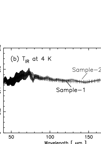
Figure 5(a) shows the far-IR transmittance of the Al-doped Ge layer at 4 K, which is obtained by dividing of Sample-1 by that of Sample-2 as shown in Fig. 5(b). Measured data distribute around ( m), whereas those for ion-implanted samples show – (e.g. Fujiwara, 2000). Thus, there is no significant far-IR absorption in the Al-doped Ge layer. In Fig. 5(b), ’s of both samples are 0.51 at m. By using the refractive index of 3.7 at 4 K, which is estimated by measuring the interference fringes around m, transmittance of the samples is calculated to be 0.50, which is in good agreement with the measured value.
The resistivity of the Al-doped Ge layer is cm at 4 K, which is consistent with that of p-type Ge with cm-3 (Fritzsche & Cuevas, 1960). Although the resistivity of the Al-doped Ge layer is much higher than that of an ion-implanted layer ( cm, Fujiwara, 2000), it meets the resistivity requirement of 38 cm for m.
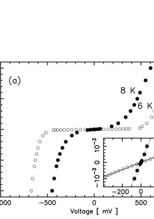
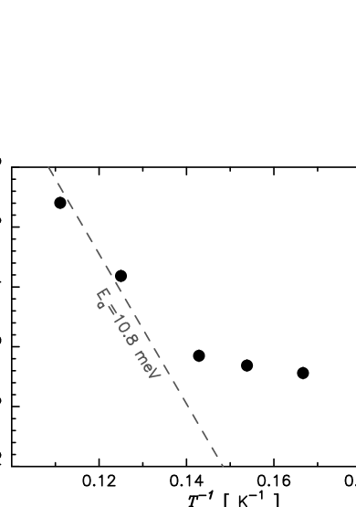
At temperatures lower than 10 K, obtained - curves in Fig. 6(a) show symmetry around mV. In particular, in the inset that shows the - curves within the range of mV, they show excellent symmetry and a linear dependence as indicated by the best-fit linear regression lines. The - curves exhibit that a linear ohmic dependence at lower voltage is followed by nonlinear increase in slope at higher voltage. These properties are typical - curves obtained for pure Ge crystals ( cm-3, Teitsworth & Westervelt, 1986). To further confirm that the - curves come from the electrical characteristic of the non-doped Ge, we investigate the relation between the current and temperature. Under low temperatures, the non-doped Ge is known to show p-type conduction that is attributed to residual gallium (Ga). Since Ga acceptors in Ge have the binding energy of 10.8 meV, the current is expected to increase with temperature in proportion to exp(). Figure 7 shows the dependence of the current on the inverse of temperature at =100 mV. At higher temperatures, the current exponentially increases with as indicated by the dashed line. Therefore, the result shows that the electrical characteristics are dominated by those of the non-doped Ge implying that an excellent ohmic contact () is realized below K.
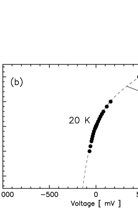
However, - curves within the temperature range of 10–20 K clearly show asymmetry around mV as seen in Fig. 6(b). Because the resistivity of the non-doped Ge exponentially decreases as temperature increases from 4 K to 10 K, the ohmic contact condition for an electrode seems to be broken (). In this condition, - curves should be asymmetric. Here, we regard an equivalent circuit for one of the Al/Ge contacts as a circuit that consists of a Schottky diode and a resistance connected in parallel; the equivalent circuit for the other Al/Ge contact is considered to be a resistance. The theoretical - curve expected from the equivalent circuit model shows the dashed line in Fig. 6(b) and fits the measured data. The result means one of the Al/Ge contacts is not the ohmic contact condition at K.
From the fact that at K, we can roughly estimate the specific contact resistance. By using the measured resistivity (10 cm) of the non-doped Ge at 10 K and considering the structure geometry of Sample-3, () is roughly estimated to be . Thus, the specific contact resistance is cm2 by multiplying with the area of the metal electrode (0.16 cm2). Under the tunneling process through a Schottky barrier (), the specific contact resistance is less sensitive to temperature (Sze & Ng, 2007). Thus, cm2 can also be applied at temperatures below 10 K and is roughly in agreement with the expected value of ( cm2) obtained from Eq.(1) with cm-3 and eV.
5 Conclusions
As a far-IR transparent electrode for Ge PCs, the Al-doped Ge layer is epitaxially formed on the non-doped Ge substrate by using the MBE technology. The activated doping concentration and layer thickness of the Al-doped Ge layer are cm-3 and 0.2 m, respectively, which are within the range of optimized solutions for the three requirements: high far-IR transmittance, low resistivity, and ohmic contact. We have evaluated the optical and electrical properties of the Al-doped Ge layer at 4 K. We obtained the far-IR transmittance of % within the wavelength range of 40–200 m, while resistivity is low enough (5 cm) compared to the requirement value of 38 cm for m. We also confirm ohmic contact between the Al-doped Ge layer and the Al electrode. We demonstrate that the MBE technology is well applicable in fabricating an excellent far-IR transparent electrode for Ge PCs.
References
- Bandaru et al. (2002) Bandaru, J., Beeman, J. W., Haller, E. E., Samperi, S., & Haegel, N. M. 2002, Infrared Phys., 43, 353.
- Beeman et al. (2007) Beeman, J. W., Goyal, S., Reichertz, L. A., & Haller, E. E., 2007, Infrared Phys., 51, 60.
- Bratt (1977) Bratt, P. R., 1977, Semiconductors and Semimetals, 12, 39.
- Fujiwara (2000) Fujiwara, M., 2000, Appl. Phys., 77, 3099.
- Fujiwara et al. (2003) Fujiwara, M., Hirao, T., Kawada, M., Shibai, H., Matsuura, S., Kaneda, H., Patrashim, M., & Nakagawa, T., 2003, Appl. Opt., 42, 2166
- Fritzsche & Cuevas (1960) Fritzsche, H. & Cuevas, M, 1960, Phys. Rev. B, 119, 1238.
- Gallacher et al. (2012) Gallacher, K., Velha, P., Paul, D. J., MacLarlen, I., Myronov, M., & Leadley, D. R. 2012, Appl. Phys. Lett., 100, 22113.
- Hadek et al. (1985) Hadek, V., Watson, D. M., & Beichman, C. A. 1985, Phys. Rev. B, 31, 3630
- Haegel et al. (1985) Haegel, N. M., Hueschen, M. R., & Haller, E. E., 1985, Infrared Phys. 25, 273
- Hiromoto et al. (1989) Hiromoto, N., Itabe, T., Aruga, T., Okuda, H., Matsuhara, H., Shibai, H., Nakagawa, T., & Saito, M. 1989, Infrared Phys., 29, 255
- Huffman & Casey (1993) Huffman, J. E., & Casey, N. L. 1993, J. Cryst. Growth 129 525.
- Kahn (1955) Kahn, A. H., 1955, Phys. Rev., 97, 1647.
- Kaneda et al. (2011) Kaneda, H., Wada, T., Oyabu, S., Kano, R., Kiriyama, R., Hattori, Y., Suzuki, T., Ide, K., Kato, M., & Watanabe, K. 2011, JaJAP, 50, 66503.
- Kazanskii et al. (1977) Kazanskii, A. G., Richards, P. L., & Haller, E. E., 1977, Appl Phys. Lett., 31, 496.
- Sun et al. (2006) Sun, S., Sun, Y., Liu, Z., Lee, D., Peterson, S., & Pianetta, P., 2006, Appl. Phys., 88, 21903.
- Sze & Ng (2007) Sze, S. M., & Ng, K. K., A Wiley-Interscience Publication, New York: Wiley, 2007, 3rd ed.
- Teitsworth & Westervelt (1986) Teitsworth, S. W. & Westervelt, R. M., 1986, Physica 23D, 181.
- Thanailakis & Northrop (1973) Thanailakis, A., & Northrop, D. C., 1973, Solid-State Electronics, 16, 1383.
- Wang et al. (1986) Wang, J. Q., Richards, P. L., Beeman, J. W., Haegel, N. M., & Haller, E. E., 1986, Appl. Opt., 25, 4127.
- Watson & Huffman (1988) Watson, D., M., & Huffman, J. E. 1988, Appl. Phys. Lett. 52, 1602.
- Watson et al. (1993) Watson, D., M., Guptill, M. T., Huffman, J., E., Krabach, T., N., Raines, S., N., & Satyapal, S. 1993, Appl. Phys. 74, 4199.
- Wu et al. (1991) Wu, I., C., Beeman, J., W., Luke, P., N., Hansen, W., L., & Haller, E., E. 1991, Appl. Phys. Lett. 58, 1431.
| Sample | Measurement | Ge substrate | Al-doped Ge layerccSizes of the Al-doped Ge and Al layers for Sample-3 are those of two split electrodes. | Al layerccSizes of the Al-doped Ge and Al layers for Sample-3 are those of two split electrodes. |
|---|---|---|---|---|
| 1 | OMaaOptical measurement, EMbbElectrical measurement | mm3 | mm3 | None |
| 2 | OM | mm3 | None | None |
| 3 | EM | mm3 | mm3 | mm3 |