Theoretical investigation of direct and phonon-assisted tunneling currents in InAlGaAs-InGaAs bulk and quantum well interband tunnel junctions for multi-junction solar cells
Abstract
Direct and phonon-assisted tunneling currents in InAlGaAs-InGaAs bulk and double quantum well interband tunnel heterojunctions are simulated rigorously using the non-equilibrium Green’s function formalism for coherent and dissipative quantum transport in combination with a simple two-band tight-binding model for the electronic structure. A realistic band profile and associated built-in electrostatic field is obtained via self-consistent coupling of the transport formalism to Poisson’s equation. The model reproduces experimentally observed features in the current-voltage characteristics of the device, such as the structure appearing in the negative differential resistance regime due to quantization of emitter states. Local maps of density of states and current spectrum reveal the impact of quasi-bound states, electric fields and electron-phonon scattering on the interband tunneling current. In this way, resonances appearing in the current through the double quantum well structure in the negative differential resistance regime can be related to the alignment of subbands in the coupled quantum wells.
pacs:
72.20.Dp,73.40.Gk,73.40.Kp,88.40.jpInterband tunnel junctions (TJ) are essential components in multi-junction solar cell devices, allowing for the series connection of single junction subcells with different band gaps as used for an enhanced utilization of the solar spectrum yamaguchi:05 ; king:07 . In a recent publication, the use of a double quantum well (DQW) structure in the junction region was shown to enhance considerably the peak tunneling current in an InAlGaAs-InGaAs TJ, at moderate loss of transparency lumb:12 . For a proper analysis of the potential of this approach and to enable further optimization of the junction design, an accurate and comprehensive theoretical description of the physical processes involved in the transport is required. However, conventional models for tunnel junction as used for the simulation of multi-junction solar cells are usually limited in this respect by a large number of simplifying assumptions on the density of states participating in the tunneling, the occupation of these states and the assisting scattering mechanisms hermle:08 ; hauser:10 .
In this paper, the tunnel junction is simulated using a rigorous quantum transport approach based on the non-equilibrium Green’s function (NEGF) formalism as used in the nano-electronics community for the simulation of interband tunneling transistors ogawa:00_2 ; rivas:01 ; rivas:03 ; luisier:10 ; knoch:10 . In combination with atomistic electronic structure theory and self-consistent coupling to a Poisson solver, the approach is able to provide a realistic picture of the relevant density of states and associated current flow under non-equilibrium conditions, by accurately reflecting the effects of internal fields, carrier confinement and elastic as well as inelastic scattering mechanisms.
| In0.52Al0.33Ga0.15As | In0.53Ga0.47As | |
| [eV] | 1.04 | 0.74 |
| [eV] | -0.14 | 0.0 |
| [eV] | 2.54 | 2.6 |
| 0.065 | 0.041 | |
| 0.087 | 0.052 | |
| 13.2 | 14.2 | |
| 10.7 | 11.0 | |
| [eV] | 0.038 | 0.033 |
| [eV] | 5 | 5 |
The present approach is based on the implementation of the NEGF formalism for III-V quantum well (QW) structures with photvoltaic applications as introduced in Ref. [ae:prb_08, ], with the material parameters of the nearest-neighbor two-band tight-binding (TB) model and interactions adjusted to the InAlGaAs-InGaAs system of Ref. [lumb:12, ], as presented in Tab. 1. The orbital basis, in difference to a band basis like , enables a consistent and unified description of electrons independent of their position in energy with respect to conduction and valence bands and is thus ideally suited for interband tunneling processes. The TB parameters are adjusted to reproduce the zone center band gaps and effective masses of the bulk component materials, choosing the light hole mass for the description of the valence band. Among the various existing scattering mechanisms for electrons and holes, elastic coupling to acoustic phonons is considered within the deformation potential approximation, and inelastic interaction with polar optical phonons is included via the corresponding Fröhlich Hamiltonian, with parameters also displayed in Tab. 1. While the former process results in a broadening of the spectral quantities in both energy and transverse momentum domain, the latter is essential for the description of the phonon mediated tunneling current at vanishing overlap of electron and hole states in the injector regions. At the present stage, no trap-assisted tunneling relying on additional defect states is included, which potentially leads to an underestimation of the dark interband current, especially at higher forward bias voltages.
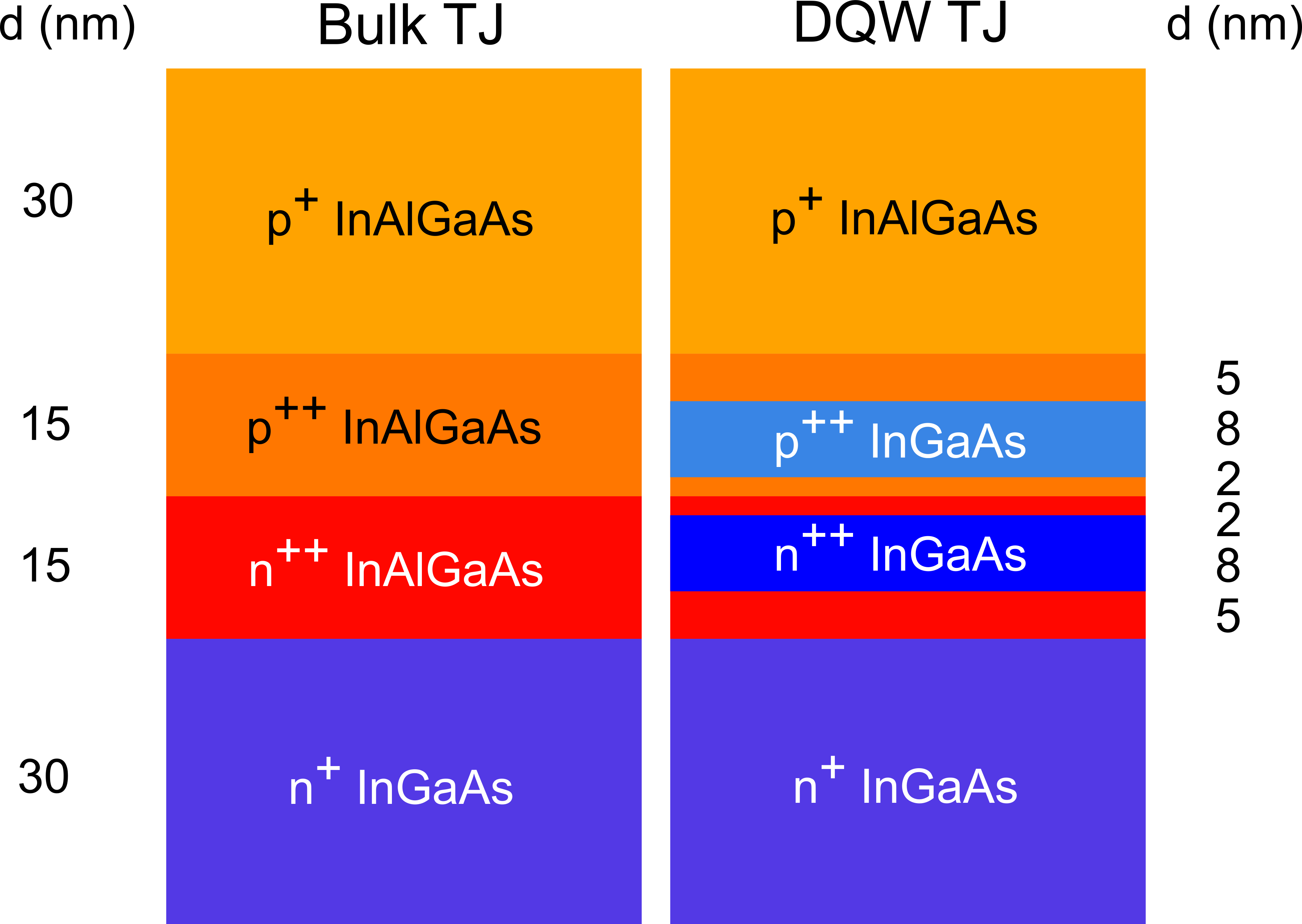
The device structures under consideration are displayed in Fig. 1 and correspond to the central region of the devices discussed in Ref. [lumb:12, ]. The tunnel junction consists of two adjacent 15 nm thick layers of In0.52Al0.33Ga0.15As with high doping level of cm-3. In the DQW structure, 8 nm of In0.53Ga0.47As are inserted on each side of the junction to form the potential wells leading to a local constriction of the interband tunneling barrier. For the present simulation, the size of the lightly doped ( cm-3) buffer layers on top and bottom of the tunnel junction is reduced to 30 nm, and neither the p-doped InGaAs capping layer nor the n-doped InP substrate present in the original structures are included.
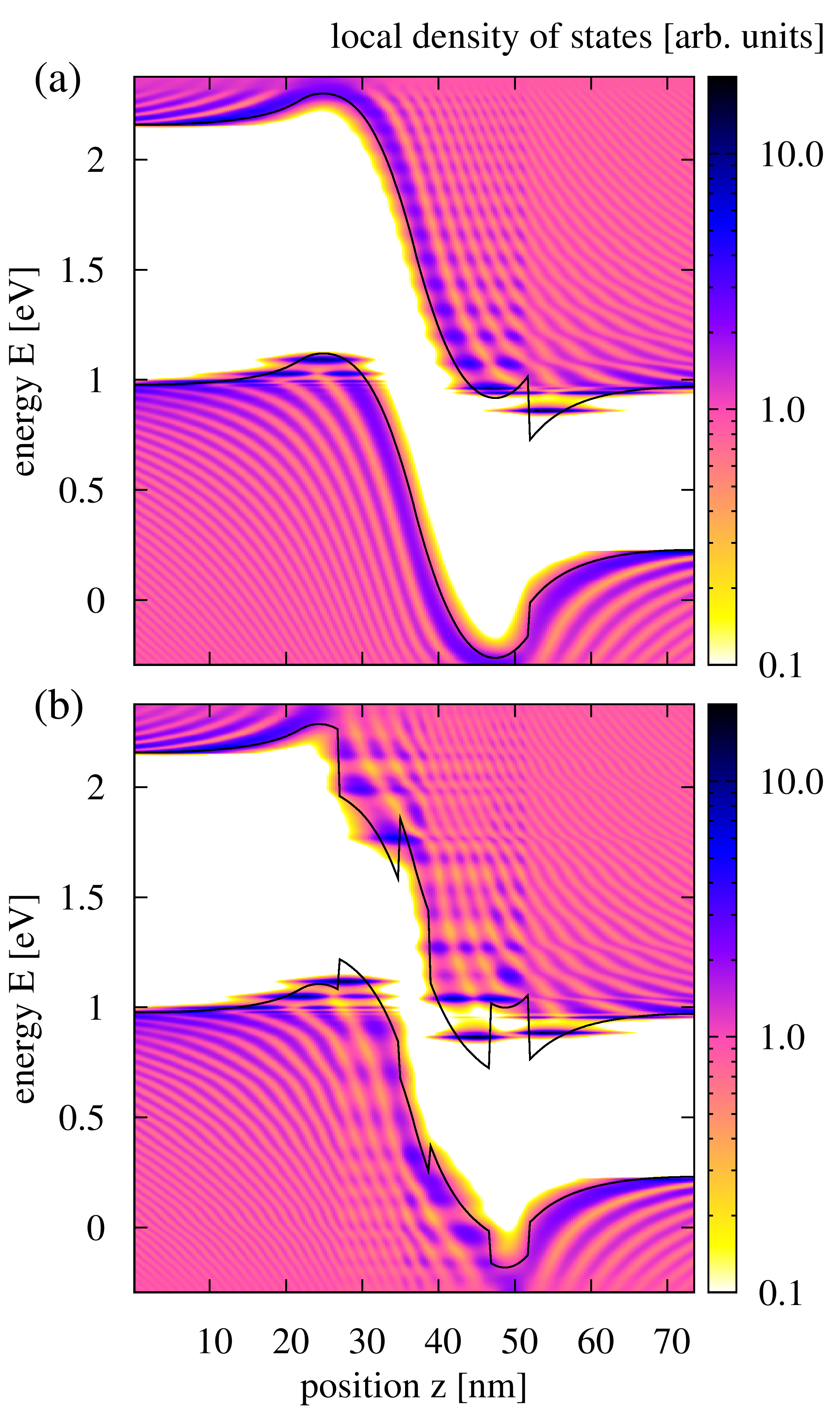
The equilibrium band edge profiles and associated local density of states (LDOS) at vanishing transverse momentum () corresponding to the above layer structures and doping levels are shown in Fig. 2. In the bulk heterojunction case, displayed in Fig. 2(a), the strong band bending close to the junction results in the appearance of bound states in both electron and hole emitter regions. While these states feed the tunneling current, they are themselves not accessible from the contacts without energy relaxation. Hence, there is only a vanishingly narrow forward bias regime with finite energetic overlap of bulk electrode states at the low doping levels of the n+ and p+ regions, where ballistic transport from one contact to the other via exclusively direct tunneling in the junction region is possible, in spite of the lower band gap at the -contact. As a consequence, any description based on a ballistic picture of direct tunneling will severely underestimate current flow even close to zero bias. There is, however, an extended forward bias regime with finite energetic overlap of interface states close to the junction via which the tunneling can proceed. In the DQW case, displayed in Fig. 2(b), both the energetic overlap and spatial extension of interface states is increased due to the presence of the additional confined subgap states in the quasi two-dimensional QW regions close to the junction. The extremely strong band bending results in a partial unbinding of the higher QW states, such that the LDOS is no longer well described by the states of a square well potential, but rather a new confinement potential reflecting the effects of both band bending and band offsets. In combination with the confined states at the heterojunction interface, the injector regions thus provide a complex combination of bound, quasibound and continuum states participating in the interband tunneling process.
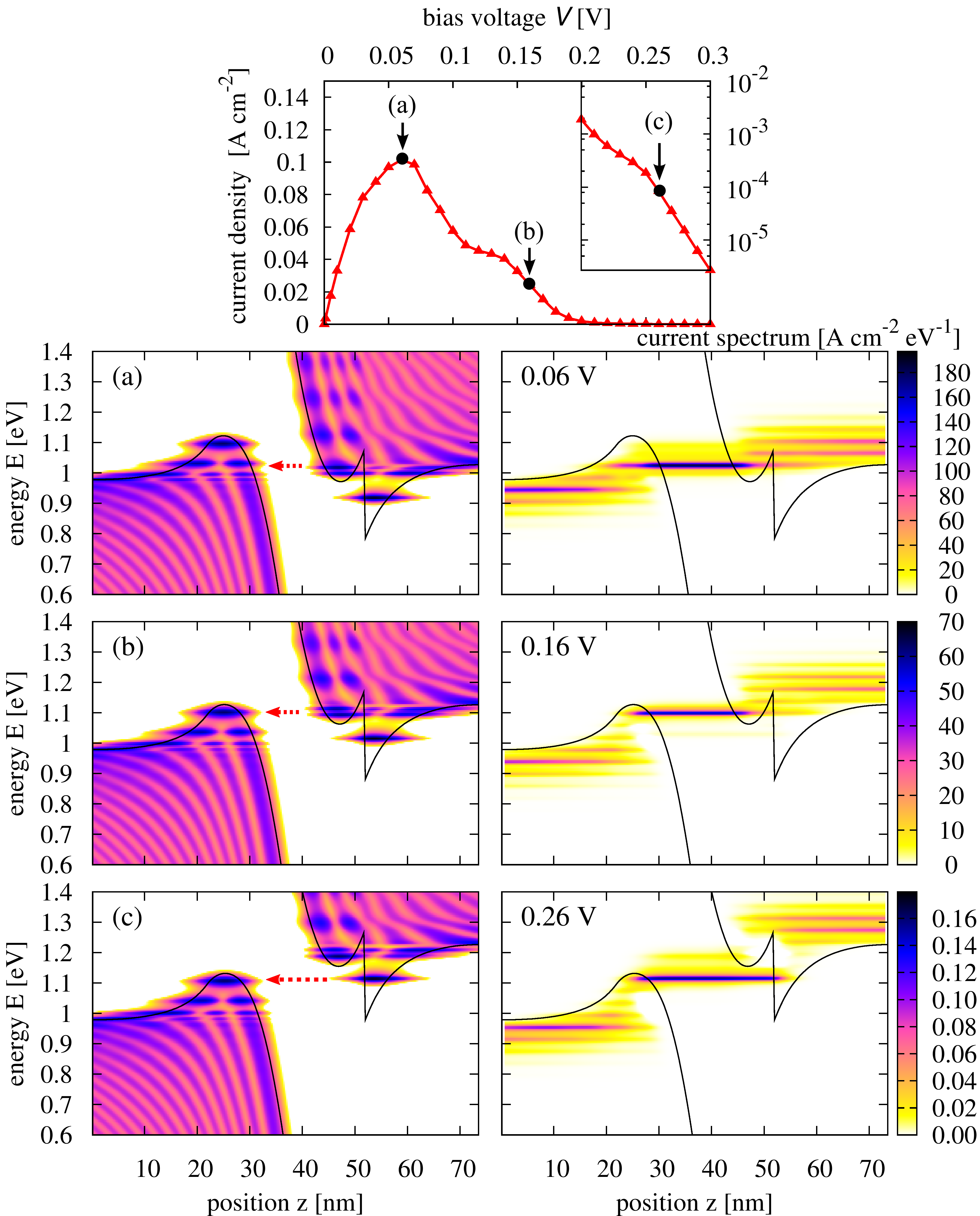
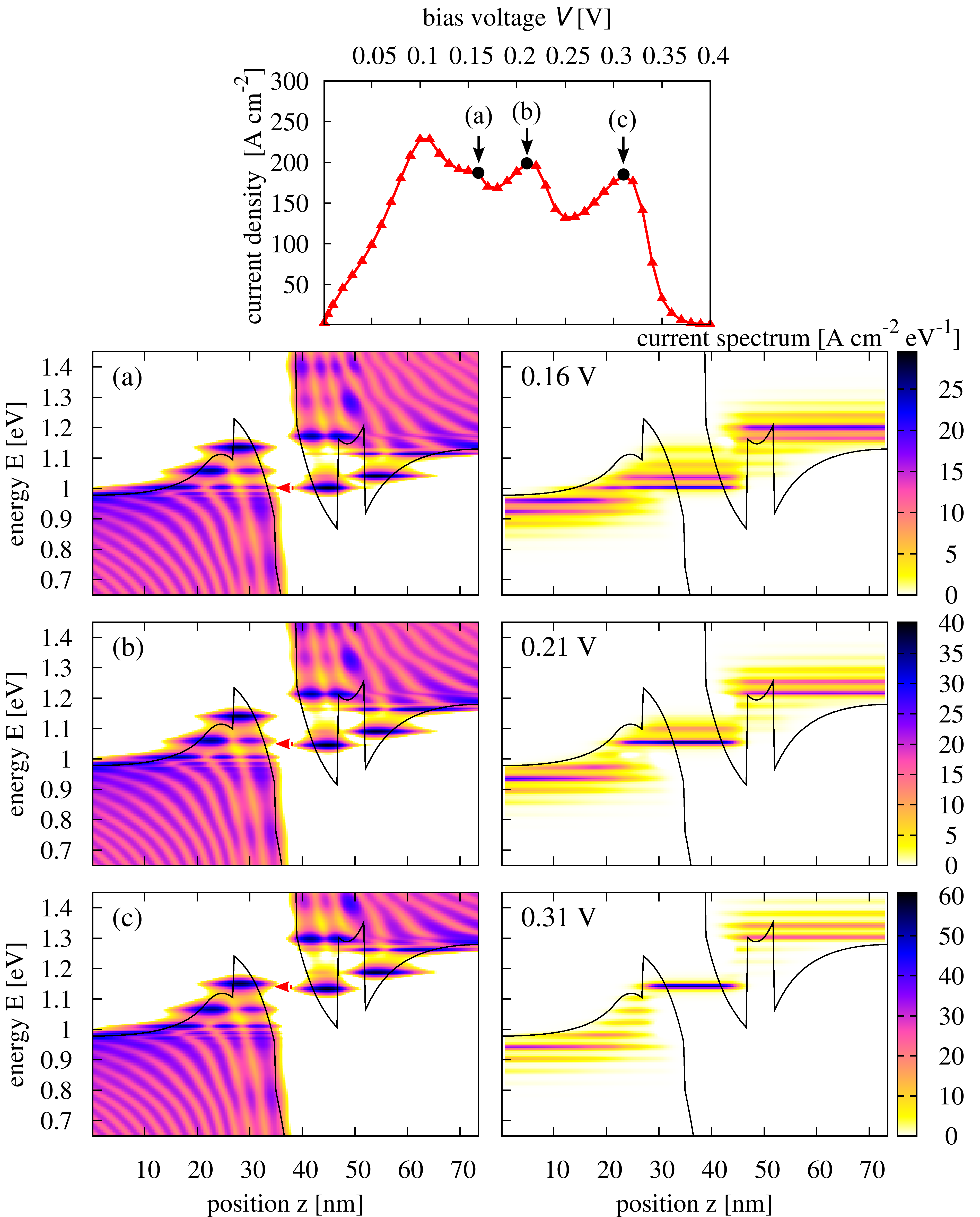
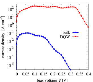
Fig. 3 displays the current-voltage characteristics of the interband charge transport in the bulk and DQW heterojunctions as computed with the NEGF model. The current-voltage characteristics reproduce the qualitative features of the experimental data in Ref. [lumb:12, ] in terms of significantly higher peak current and peak voltage, resulting from the lower effective barrier potential, but lower negative differential resistance (NDR) for the DQW TJ as compared to the bulk TJ. As can be inferred from Fig. 2 (a), the structure appearing in the NDR region of the IV characteristics for the bulk heterojunction is due to discretization of the longitudinal DOS in the injection regions adjacent to the junction. In the DQW sample, the local current maxima are much more pronounced and are identified as the signatures of resonant tunneling between different QW states.
In order to analyze the current flow in the two structures in more detail with respect to the different extended and localized states involved, the current spectrum at different bias voltage is computed for the full spatial extent of the device. In the case of the bulk heterojunction, the result displayed in Fig. 4, together with the corresponding LDOS (), allows the distinction of different regimes of interband charge transport depending on the applied bias: (a) At the peak voltage of 0.06 V, current flow is dominated by carriers first tunneling through the triangular barrier of the hetero-interface at the electron contact into the lowest subband of the doping-induced potential well at the n-side of the junction and then into the second subband of the doping-induced potential well at the p-side, from where escape to the hole contact proceeds via electron-phonon scattering. A minor contribution is due ballistic transport above the triangular barrier into the subband associated with the lowest localized state at the p-side; (b) At a bias of 0.16 V, after initial relaxation close the contacts mediated by multiple scattering events with phonons, current flow proceeds again predominantly via tunneling through the triangular barrier from the n-side, but now into the lowest subband of the doping-induced potential well at the p-side; (c) At even larger bias voltage of 0.26 V, the major part of the current flows via the lowest subband of the triangular potential well at the hetero-interface into the lowest subband at the p-side, overcoming a substantially thicker tunneling barrier, while only a small fraction of carriers are transported via phonon-assisted tunneling from the higher interface states. Beyond this transport regime, i.e., for considerably larger separations of contact Fermi levels, there are no more available current paths in terms of energetically overlapping states in the injection regions, and current breaks down exponentially, until thermionic emission sets in, or, in more realistic cases, defect-assisted tunneling takes over. In the DQW TJ, as shown in Fig. 5 the dominant role in the transport process is played by the QW states, which in case of energetic alignement at specific values of the bias voltage give rise to resonant tunneling. On the n-side, current flow proceeds over the whole bias regime via tunneling into the second subband of the QW and subsequent relaxation into the lowest subband, while the states in the triangular well at the heterointerface seem to be irrelevant for transport. On the p-side, there is a strong bias dependence of the specific subband involved in the interband tunneling process: (a) at 0.16 V, the alignement is between the lowest subband at the n-side and the third subband state at the p-side, (b) at 0.21 V, the second subband is resonant and (c) at 0.31 V, carriers are transferred between the lowest subbands of the QW. Again, beyond this point, energetic overlap is limited to phonon sidebands, which results in an exponential decay of the current with increasing forward bias voltage. Finally, in both tunnel junction devices, due to the prominent role of narrow bands with enhanced transmission, the current spectrum close to the contacts shows a pronounced structure depending on the phonon energy, in spite of the bulk-like, continuous DOS in these regions.
In conclusion, we have presented a rigorous approach to the simulation of carrier transport in interband tunnel junctions with applications in multi-junction solar cells, which is able to account for both direct and phonon-assisted contributions under consideration of realistic spatial potential variations, including arbitrarily shaped quantum well structures. By consideration of the local maps of DOS and current spectrum, a microscopic picture of the current flow at different values of forward bias voltage is obtained. Apart from providing insight into the dominant transport mechanisms at given bias, the simulation results are in qualitative agreement with the experimentally found large increase in peak current and peak voltage as well as a decrease of NDR by the insertion of a double quantum well structure in the junction region. The quantitative agreement of the tunneling currents with the measured values is expected to be improved by the use of a larger tight-binding basis such as jancu:97 , a more accurate treatment of the scattering processes and, most notably, the inclusion of defect-assisted tunneling processes. The latter is essential to extend the present approach to multi-junction solar cell devices based on disordered and defect-rich materials, such as the micromorph silicon thin-film tandem solar cell.
References
- (1) M. Yamaguchi, T. Takamoto, K. Araki, and N. Ekins-Daukes, Sol. Energy 79, 78 (2005)
- (2) R. R. King, D. C. Law, K. M. Edmondson, C. M. Fetzer, G. S. Kinsey, H. Yoon, R. A. Sherif, and N. H. Karam, Applied Physics Letters 90, 183516 (2007),
- (3) M. P. Lumb, M. K. Yakes, M. González, I. Vurgaftman, C. G. Bailey, R. Hoheisel, and R. J. Walters, Applied Physics Letters 100, 213907 (2012),
- (4) M. Hermle, G. Létay, S. P. Philipps, and A. W. Bett, Progress in Photovoltaics: Research and Applications 16, 409 (2008),
- (5) J. R. Hauser, Z. Carlin, and S. M. Bedair, Applied Physics Letters 97, 042111 (2010),
- (6) M. Ogawa, R. Tominaga, and T. Miyoshi, Simulation of Semiconductor Processes and Devices (SISPAD), 66(2000)
- (7) C. Rivas, R. Lake, G. Klimeck, W. R. Frensley, M. V. Fischetti, P. E. Thompson, S. L. Rommel, and P. R. Berger, Appl. Phys. Lett. 78, 814 (2001),
- (8) C. Rivas, R. Lake, W. R. Frensley, G. Klimeck, P. E. Thompson, K. D. Hobart, S. L. Rommel, and P. R. Berger, J. Appl. Phys. 94, 5005 (2003),
- (9) M. Luisier and G. Klimeck, Journal of Applied Physics 107, 084507 (2010),
- (10) J. Knoch and J. Appenzeller, Electron Device Letters, IEEE 31, 305 (april 2010),
- (11) U. Aeberhard and R. Morf, Phys. Rev. B 77, 125343 (2008)
- (12) J. M. Jancu, R. Scholz, F. Beltram, and F. Bassani, Phys. Rev. B 57, 6493 (1998)