e-mail adyrdal@amu.edu.pl, Phone: +48-61-8296 396, Fax: +48-61-8295 298
2 Institute of Molecular Physics, Polish Academy of Sciences, ul. M. Smoluchowskiego 17, 60-179 Poznań, Poland
XXXX
Intrinsic spin Hall effect in silicene: transition from spin Hall to normal insulator
Abstract
\abstcolIntrinsic contribution to the spin Hall effect in a two-dimensional silicene is considered theoretically within the linear response theory and Green function formalism. When an external voltage normal to the silicene plane is applied, the spin Hall conductivity is shown to reveal a transition from the spin Hall insulator phase at low voltages to the conventional insulator phase at higher voltages. This transition resembles recently reported phase transition in a bilayer graphene. The spin-orbit interaction responsible for this transition in silicene is much stronger than in graphene, which should make the transition observable experimentally.
keywords:
spin transport, spin Hall effect, silicene1 Introduction
There is currently a great interest in two-dimensional IVA materials like graphene and silicene. The peculiar electronic transport properties of these materials, which follow from their unusual band structure, make them promising for applications in future nanoelectronics. As the properties of graphene are already rather well known [1, 2], the silicene – a two-dimensional silicon lattice – has been synthesized only very recently [3] and attracts great attention both theoretical and experimental [4].
Similarly to graphene, the silicene is a material with linear electronic energy spectrum near the Fermi level. The intrinsic spin-orbit interaction, however, opens an energy gap, which in silicene is relatively wide. The corresponding intrinsic gap in graphene is rather negligible and therefore the effects due to its presence are not observable experimentally. The large energy gap as well as compatibility with silicon-based conventional electronics make the silicene a very interesting material – also for spin electronics.
In this paper we study the spin Hall effect [5, 6] in silicene, induced by intrinsic spin-orbit interaction. This contribution to the spin Hall conductivity follows from a nontrivial trajectory of charge carriers in the momentum space due to the spin-orbit contribution of a perfect crystal lattice to the corresponding band structure, and therefore it is also called topological spin Hall effect (for review of SHE see e.g. Refs. [7, 8]).
The buckled structure of silicene (see Fig.1) makes the corresponding spin-orbit interaction rather strong. Moreover, in additon to the usual intrinsic spin-orbit interaction, there is also an intrinsic Rashba like term, and both terms contribute to the spin Hall conductivity. For simplicity, we neglect here the role of structural defects, assuming perfect crystalline two-dimensional lattice. As in the case of graphene, the spin Hall conductivity is shown to be finite when the Fermi level is in the gap. Since the Rashba type interaction is rather small, the intrinsic spin Hall conductivity in silicene is almost quantized. We also show that electric field (gate voltage) normal to the silicene plane leads to a transition from the spin Hall insulator phase to the normal insulator state, in agreement with predictions by Ezawa [9, 10]. We also note that the transverse spin current in systems with spin-orbit coupling may be generated by a temperature gradient instead of electric field, and the effect is then known as thermal spin Hall or spin Nernst effect.
2 Model
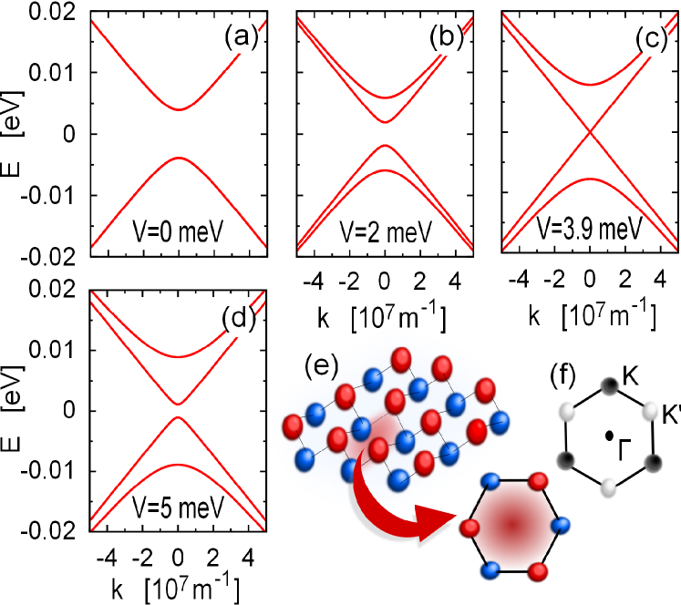
The crystallographic structure of silicene is shown schematically in Fig.1 and is similar to graphene except that the planes corresponding to the two atomic sublattices are now spatially separated. The buckled atomic arrangement has two important consequences. First, such a structure gives rise to a relatively large intrinsic spin-orbit coupling responsible for a sizable energy gap. This spin-orbit coupling also includes the Rashba like term. Second, since the planes of the corresponding two sublattices are separated, by applying perpendicular voltage one can modify and control the electronic band structure. In the following considerations we calculate the spin Hall conductivity taking into account both terms in the intrinsic spin-orbit coupling as well as the effects due to perpendicular external voltage.
To describe electronic states in silicene we use an effective Hamiltonian that was derived within the tight-binding method and first-principle calculations [11]. In the sublattice space, the matrix form of this Hamiltonian for the K point of the Brillouin zone takes the form
| (1) |
where with being the Fermi velocity, and
| (2) |
The parameters and describe the two terms of the intrinsic spin-orbit interaction, is the perpendicular voltage (in energy units), and are the unit () and Pauli () matrices in the spin space. The corresponding energy spectrum near the K point is shown in Fig.1(a-d) for indicated gate voltages. It is evident that gate voltage first closes the gap and then opens it again when increases further.
Density of spin current in the silicene plane can be written as (for ), where is the spin conductivity with being the -th component () of electron spin, and is the th component of the in-plane electric field. The quantum-mechanical operator of spin current density may be defined as , where is the velocity operator (). In the linear response theory, the zero-frequency spin Hall conductivity is given by the formula [12],
| (3) |
where is the Green function corresponding to the Hamiltonian (1) of the system.
3 Spin Hall conductivity
We consider now spin Hall conductivity, separately for the case without vertical bias and for the case with a vertical voltage applied. Let us begin with the former case.
The case of
Calculating the appropriate Green functions and following the general procedure [12], one finds the spin Hall conductivity from Eq.(3). When the Fermi level (measured fom the middle of the gap) is located either in the valence or conduction bands, the spin Hall conductivity is given by
| (4) |
When, in turn, the Fermi level is inside the energy gap, one finds
| (5) |
One can note, that due to the intrinsic Rashba type spin-orbit coupling, the spin Hall conductivity for the Fermi level in the energy gap is generally not quantized. However, the parameter meV in silicene is relatively small, so the main contribution to the spin-orbit coupling is due to the term proportional to . Indeed, assuming the relevant parameters one finds . Thus, the influence of intrinsic Rashba spin-orbit interaction on the spin Hall conductivity is rather minor and will be neglected in the following. Accordingly, assuming one may rewrite Eqs (4) and (5) as
| (6) |
| (7) |
for the Fermi level in the conduction/valenece bands and in the energy gap, respectively. The latter formula shows that spin Hall effect in silicene is quantized when the Fermi level is in the gap.
3.1 SHE with biased voltage
When the external vertical voltage is applied, one finds
| (8) |
if the Fermi level crosses both valence or both conduction bands, . In turn, the spin Hall conductivity for is given by
| (9) |
while for the Fermi level inside the energy gap, , one finds
| (10) |
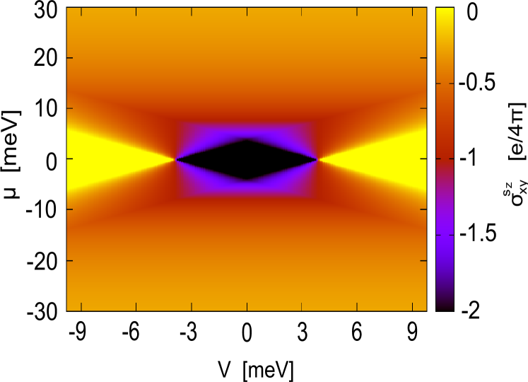
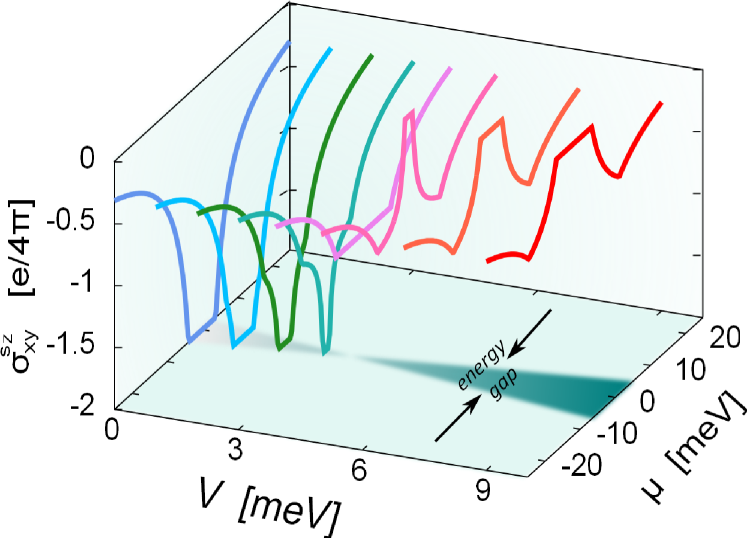
Behavior of the spin Hall conductivity with increasing voltage and position of the Fermi level is shown in Fig.2, where contributions from both points of the Brillouin zone are included. This figure clearly shows that the energy gap, where the spin Hall conductivity is finite and quantized, shrinks with increasing voltage . At some critical value of the gap becomes closed, and then opens again with increasing further. However, the spin Hall conductivity vanishes then for in the gap. This behavior is also evident in Fig.3, where some cross-sections of Fig.2 for selected values of the voltage are plotted. Both figures clearly indicate a transition from spin Hall insulator phase at voltages smaller than the critical voltage to conventional insulating behavior at voltages larger than the critical one.
4 Summary
To summarize, we have derived some analytical formula for spin Hall conductivity in silicene due to intrinsic spin-orbit interaction. We have shown that the intrinsic Rashba type term in spin-orbit interaction has a negligible influence on the spin Hall conductivity, so the latter is quantized when the Fermi level is inside the gap. Furthermore, we have shown that there is a transition from the spin Hall insulator phase to the conventional insulator one with increasing external gate voltage applied perpendicularly to the layer plane.
This work has been supported by the European Union under European Social Fund - Operational Programme ’Human Capital’ - POKL.04.01.01-00-133/09-00.
References
- [1] A. H. Castro Neto, F. Guinea, N. M. R. Pers, K. S. Novoselov, and A. K. Geim, Rev. Mod. Phys. 81, 109 (2009).
- [2] D. S. L. Abergel, V. Apalkov, J. Berashevich, K. Ziegler, and T. Chakraborty, Advances in Physics, 59, No. 4, 261 (2010).
- [3] B. Lalmi, H. Oughaddou, H. Enriquez, A. Kara, S. Vizzini, B. Ealet, and B. Aufray, Appl. Phys. Lett. 97, 223109 (2010).
- [4] A. Kara, H. Enriquez, A. P. Seitsonen, L. C. L. Y. Voon, S. Vizzini, B. Aufray, H. Oughaddou, Surface Science Reports 67, 1-18 (2012).
- [5] M. I. Dyakonov, V. I. Perel, Pis’ma Z. Eksp. Teor. Fiz. 13, 657 (1971); JETP Lett. 13, 467 (1971).
- [6] J. E. Hirsch, Phys. Rev. Lett. 83, 1834 (1999).
- [7] H. A. Engel, E. I. Rashba, B. I. Halperin, in Handbook of Magnetism and Advanced Magnetic Materials, edited by H. Kronmuller, S. Parkin, vol. 5: Spintronics and Magnetoelectronics, John Willey, New York, 2007.
- [8] M. I. Dyakonov and A. V. Khaetskii, in Spin Physics in Semiconductors edited by M. I. Dyakonov, Chap. 8, Springer-Verlag, Berlin, Heidelberg, 2008.
- [9] M. Ezawa, arXiv:1201.3687v1 (2012).
- [10] M. Ezawa, arXiv:1202.1357 (2012).
- [11] C.-C. Liu, H. Jiang, and Y. Yao, Phys. Rev. B 84, 195430 (2011).
- [12] A. Dyrdał, V.K. Dugaev, J. Barnaś, Europhysics Letters 85, 67004 (2009)