Supplemental Material
Gate-tuned two-channel Kondo screening by graphene leads:
Universal scaling of the nonlinear conductance
Tsung-Han Lee1, Kenneth Yi-Jieh Zhang1, Chung-Hou Chung1,2, Stefan Kirchner3,41Department of Electrophysics, National Chiao-Tung University,
HsinChu, Taiwan, 300, R.O.C.
2National Center for Theoretical Sciences, HsinChu, Taiwan, 300, RO.C.
3Max-Planck-Institut für Physik komplexer Systeme, 01187 Dresden, Germany
4Max-Planck-Institut für chemische Physik fester Stoffe, 01187 Dresden, Germany
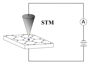
Figure 1: The STM measurement of the magnetic adatom in graphene.
The magnetic adatom is located at the center of the honeycomb lattice
of graphene.
I A: Non-equilibrium NCA
The extension of the non-crossing approximation onto the Keldysh contour has been discussed
in several papers kroha ; Meir . It is customary to neglect the bias voltage dependence of the conduction electron density of states (DOS) ,
This is justified provided is well approximated by a constant in a region around the
Fermi energy that is large compared to the applied bias voltage. When the DOS vanishes in a power-law fashion at or near the Fermi energy,
this is no longer possible and the equations have to be generalized appropriately.
The full set of equations to be solved for the two-channel pseudogap problem becomes
for the pseudo-boson and
for the pseudo-fermion. The DOS ( and ) of the two leads do not have to be identical.
The bias voltage applied across the system is
, where and are the chemical potentials of the left and right leads.
II B: Fano-lineshapes
An experiment reminiscent of the situation considered by us has been performed recently, where
magnetic adatoms on graphene where investigated via scanning tunneling microscopy (STM), see Ref. Mattos, .
Our analysis can be extended to include the current-voltage characteristics measured by an STM (see Fig.1). In this case,
one of the two fermionic leads represents the STM tip and it is necessary to explicitly allow for the different tunneling paths between the STM tip, the
adatom and the substrate which will act as the second lead. An important difference between the STM setup and our analysis so far is that
the STM tip is a good metal, e.g. a single-channel lead with constant DOS at its Fermi energy. We here will model it by a two-channel lead with constant
DOS at its Fermi energy. This is justified provided the coupling between the STM tip and the system is small as the RG scaling equations for two and one-channel
case are identical up to fourth order in the tunneling matrix element.
The theory of STM on
magnetic adatoms on a metal surfaces has been worked out by Schiller and Hershfield Schiller and by
O. Újsághy et al. Ujsaghy .
The current is obtained from
(1)
where is the density of states of the STM tip and is an effective density of states probed by the STM and depends on two tunneling rates and that parameterize the hybridization
strength of the STM tip with the magnetic adatom () and the graphene leads (). The effective density of states
can be recast into
(2)
where is the hybridization strength between the graphene electrons and the magnetic adatom, is the advanced local graphene electron
Green function at the locus of the
STM tip and is the advanced graphene electron Green function connecting the locus of
the tip with the position of the adatom at , and () is the tunneling matrix element between the STM tip and the substrate
(magnetic adatom).
is the advanced Green function of the magnetic adatom that can be obtained from the pseudo-particle Green functions of section A.
In the linear regime, the Fano lineshape is given by the
differential conductance , which turns out to be
proportional to the effective density of states :
.
can be cast into the Fano lineshape where the Fano parameter q is given by Ujsaghy ; Fano ; chung
(3)
and can be treated as approximately constant in the energy range of interest Fano .
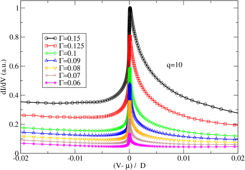
Figure 2: Fano-lineshapes with Fano parameter for various values of (in units of the half-bandwidth
). Here, we have set , .Figure 3: Non-linear conductance for a large between
impurity and graphene substrate and a much smaller hoping
between tip and the impurity, ,
corresponding to the STM measurement reported in Mattos .
The curves agree well with the
STM results of Mattos . (a) dependence around .
(b) behavior for . (c) 2CK behavior for . Here,
.
The other parameters are: , .
Typical Fano-lineshapes in the linear regime
are shown in Fig. 2.
The 2CK behavior seen in the STM measurement Mattos
for Co-adatom at the center of the honeycomb lattice
is signaled by the Kondo peaks at in Fano-lineshapes,
which are compatible with a large fitting parameter (for example )
and a correspondingly small and concomitantly small intervalley scattering.
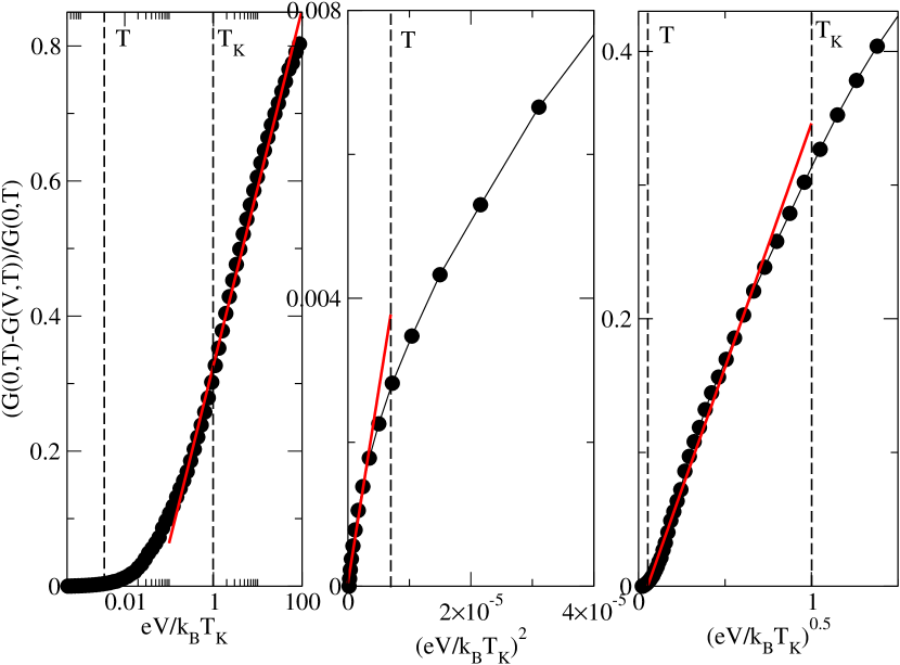
Figure 4: Universal scaling in linear conductance as a function
of temperature for at fixed
positive chemical potential and for various values of
hybridization . (a) 2CK behavior for for
large values of .
Inset: vs.
.
(b) Universal scaling of for smaller values of .
Inset: The crossover energy scale as a power-law function of
.
Here, , is the linear conductance for
at , and .
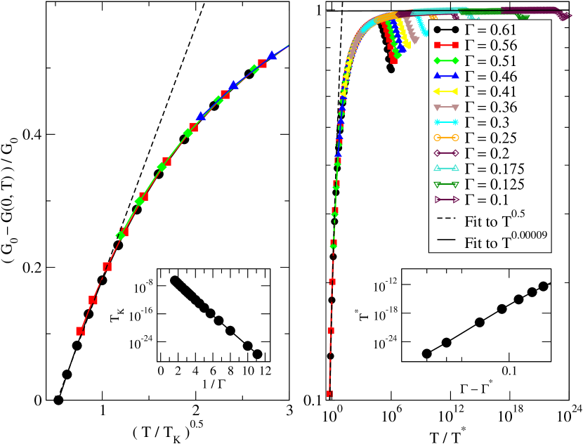
III C. Universal 2CK-LM crossover for
In the main text, we focus on the universal 2CK-LM crossover
for negative chemical potential, .
A similar scaling behaviors can also be found
in conductance for positive . As shown in Fig. 4,
for a fixed positive , the linear conductance
vs. hybridization follows a
single universal scaling form of . The single scaling form of
we observe here for is somewhat surprising as for
the conductance shows two distinct scaling regimes: and
. We believe that this difference maybe due to
the particle-hole asymmetry in our model as the Kondo peak, located
at , is affected more by the charge peak at .
for than that for .
Similar to the case for , the linear conductance
for shows a typical 2CK behavior for
, and a universal power-law behavior at high temperatures
for :
with .
The Kondo temperature and the crossover scale
for behave in a similar way to their counterparts:
,
with
and . We believe that our results
for both positive and negative values of could be used as theoretical
guidance in future experiments to clarify the issue on two-channel
Kondo physics in graphene.
References
(1)
Matthias H. Hettler, Johann Kroha, and Selman Hershfield, Phys.
Rev. Lett. 73, 1967 (1994); Ch. Kolf, J. Kroha, M. Ternes, and W.-D. Schneider, Phys. Rev. Lett. 58, 5649 (1998).
(2)
Ned S. Wingreen and Y. Meir, Phys. Rev. B 49, 11040 (1994).
(3)
A. Schiller and S. Hershfield, Phys. Rev. B 61, 9036 (2000).
(4)
O. Újsághy et al.
Phys. Rev. Lett. 85, 2557 (2000).
(5)
U. Fano, Phys. Rev. 124, 1866–1878 (1961).
(6)
Chung-Hou Chung and Tsung-Han Lee, Phys. Rev. B 82, 085325 (2010)
(7)
L. S. Mattos et al., (un-published).
(8)
V. Madhavan, W. Chen, T. Jamneala, M. F. Crommie, and N. S. Wingreen,
Phys. Rev. B 64, 165412 (2001).