Graphene and Some of its Structural Analogues: Full-potential Density Functional Theory Calculations
Gautam Mukhopadhyay***Corresponding author’s E-mail: gmukh@phy.iitb.ac.in; g.mukhopa@gmail.com and Harihar Behera†††E-mail: harihar@phy.iitb.ac.in; behera.hh@gmail.com
Department of Physics, Indian Institute of Technology, Powai, Mumbai-400076, India
Abstract
Using full-potential density functional calculations we have investigated the structural and electronic properties of graphene and some of its structural analogues, viz., monolayer (ML) of SiC, GeC, BN, AlN, GaN, ZnO, ZnS and ZnSe. While our calculations corroborate some of the reported results based on different methods, our results on ZnSe, the two dimensional bulk modulus of ML-GeC, ML-AlN, ML-GaN, ML-ZnO and ML-ZnS and the effective masses of the charge carriers in these binary mono-layers are something new. With the current progress in synthesis techniques, some of these new materials may be synthesized in near future for
applications in nano-devices.
Keywords : Graphene, Graphene-like materials, 2D crystals, Electronic structure, Firstprinciples calculations
1 Introduction
Graphene is a crystal of carbon (C) atoms tightly
bound in a two dimensional (2D) hexagonal lattice.
It is a monolayer of carbon atoms (ML-C), i.e., one atom
thick. The exotic properties of this 2D material
were revealed only in 2004-2005 by a series of
papers coming from the Manchester [1, 2, 3] and Columbia [4] groups.
The unambiguous synthesis (by mechanical
exfoliation of graphite), identification (by
transmission electron microscopy (TEM)) and
experimental determination of some of the exotic
properties of graphene were reported first in 2004, by the
Manchester group led by Novoselov and Geim [1].
In 2010, Konstantin S. Novoselov and Andre Geim were awarded the
Nobel Prize in Physics for the “groundbreaking
experiments regarding the two-dimensional material
graphene”. However, graphene research has a history
which dates back to the 1859 work of Brodie [5, 6, 7, 8].
The term graphene was introduced by
Boehm and his colleagues in 1986 [9]. Graphene “graph” “ene”
and the term “graph” is derived from the word “graphite” and
the suffix “ene” refers to polycyclic aromatic hydrocarbons. Now graphene is considered as the basic building block of graphitic materials (i.e.,
graphite stacked graphene, fullerenes wrapped graphene, nanotube rolled graphene, graphene nanoribbon nano-scale finite area sized
rectangular graphene).
The existence of free-standing 2D crystals were
believed impossible for several years, because they
would ultimately turn into a three-dimensional (3D)
objects as predicted by Peierls [10],
Landau [11] and Mermin [12]. The theoretical reason for this is that at finite
temperatures, the displacements due to thermal
fluctuations could be of the same magnitude as the
inter-atomic distances, which make the crystal
unstable. Further, experimentally one generally
finds that thin films cannot be synthesized below a
certain thickness, due to islands formations or even
decomposition. Hence, the synthesis of graphene [1]
was surprising which put a
question mark on the predictions of Peierls, Landau
and Mermin. However, this issue was (at least
partially) solved when it was shown that freestanding
graphene sheets display spontaneous
ripples owing to thermal fluctuation [13],
and therefore real graphene is not perfectly flat. It is
important to note that such instabilities are the result
of thermal fluctuations which disappear at
temperature T K. This aspect will be used later
in our discussions on the study of the stability of
graphene and some of its structural analogues
reported here on the basis of their ground state (i.e.,
T K) total energies.
Being a one-atom-thick planar crystal of C atoms,
graphene is the thinnest nano-material ever known.
It has exotic mechanical, thermal, electronic, optical
and chemical properties, such as the high carrier
mobility, a weak dependence of mobility on carrier
concentration and temperature, unusual quantum
hall effect, hardness exceeding 100 times that of the
strongest steel of same thickness and yet flexible
(graphene can sustain elastic tensile strain more
than without breaking, and is brittle at certain
strain limit), high thermal conductivity comparable
to that of diamond and 10 times greater than that of
copper, negative coefficient of thermal expansion
over a wide range of temperature. Because of these
properties graphene has potentials for many novel
applications [6, 7, 14, 15, 16, 17, 18, 19, 20].
The rapid advancements of nanotechnology and the computing power have
enabled the researchers in the field to explore the
unusual properties of graphene from many
perspectives of application and fundamental
science. The study of graphene is possibly the
largest and fastest growing field of research in
material science.
The impressive growth in the
research on graphene has inspired the study of other
graphene-like 2D materials [20, 21]. For instance, a
number of 2D/quasi-2D nanocrystals (not based on
carbon) have been synthesized or predicted
theoretically in recent years. Representative samples
of other 2D nanocrystals which have been
synthesized include BN, MoS2, MoSe2, Bi2Te3 [20, 21],
Si [22], ZnO [23]. Recently, the density functional theory (DFT)
calculations of Freeman group [24] have shown that when
the layer number of (0001)-oriented wurtzite (WZ) materials (e.g., AlN,
BeO, GaN, SiC, ZnO and ZnS) is small, the WZ
structures transform into a new form of stable
hexagonal BN-like structure. This prediction has
recently been confirmed in respect of ZnO [23],
whose stability is attributed to the strong inplane
sp2 hybridized bonds between Zn and O
atoms. Graphene-like 2D/quasi-2D honeycomb
structures of group- and binary compounds
have also been studied [25, 26] by using
pseudo-potential DFT calculations. Here, we report our
calculations on the structural and electronic properties
of graphene and some other graphene-like monolayer
(ML) structures of the binary compounds, viz.,
SiC, GeC, BN, AlN, GaN, ZnO, ZnS, ZnSe using the DFT.
2 Computational Methods
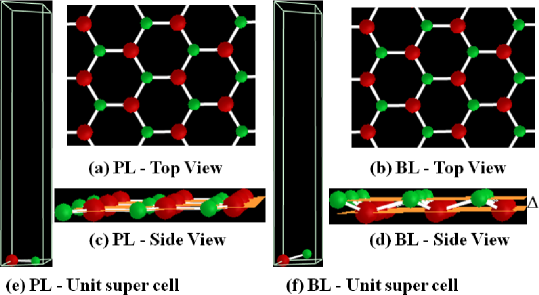
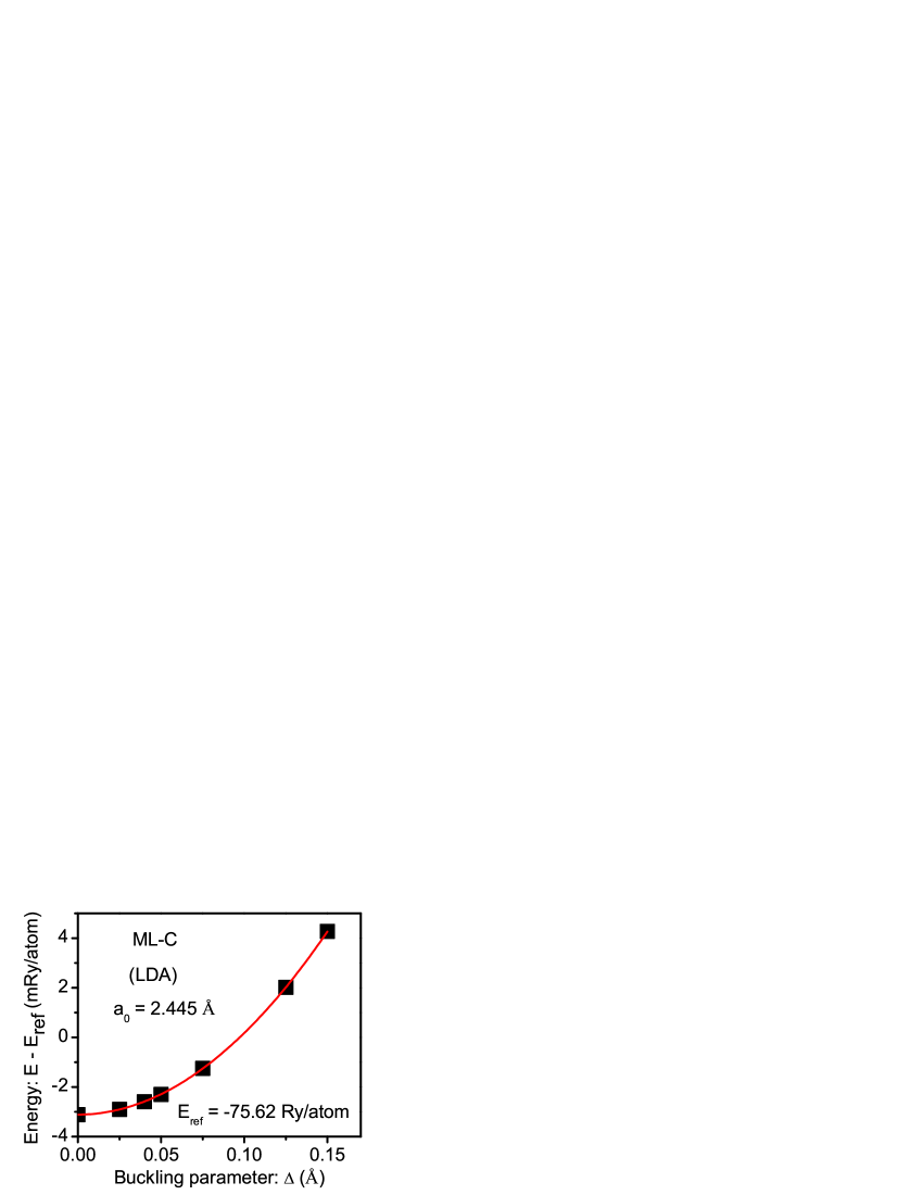
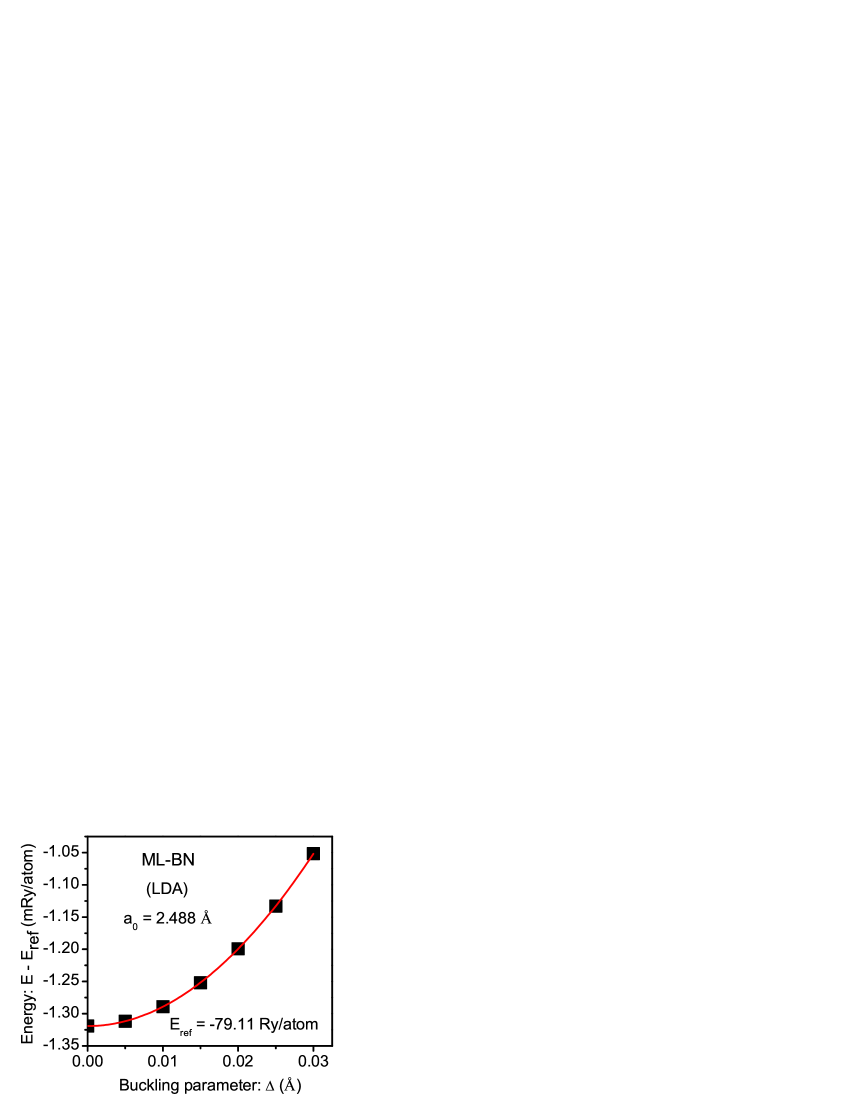
We use the DFT based full-potential (linearized) augmented plane wave plus local orbital (FP-(L)APW+lo) method [27, 28, 29] as implemented in the elk-code (http:// elk.sourceforge.net/) and the Perdew-Zunger [30] variant of local density approximation (LDA) for our calculations. The accuracy of this method and code has been successfully tested in our previous studies [31, 32, 33, 34, 35, 36, 37]. For plane wave expansion in the interstitial region, we have used , where is the smallest muffin-tin radius, for deciding the plane wave cut-off. The Monkhorst-Pack [38] -point grid size of was used for structural and of for band structure and total density of states (TDOS) calculations. The total energy was converged within 2 eV/atom. The 2D-hexagonal structure was simulated by a 3D-hexagonal super cell with a large value of -parameter ( a.u.) as shown in Figure 1. For structure optimization, we have considered two different structures, viz., (i) Planar structure (PL) and (ii) Buckled structure (BL) as shown in Figure 1 for a monolayer of BN (ML-BN), which is the prototype of all the materials considered here (for graphene, B and N atoms are to be replaced by the C atoms).
3 Results and Discussions
We have optimized the 2D hexagonal structures
of graphene (ML-C) and the mono-layers of SiC
(ML-SiC), GeC (ML-GeC), BN (ML-BN), AlN
(ML-AlN), GaN (ML-GaN), ZnS (ML-ZnS) using
the principle of minimum energy for the stable
structure as per the following procedure. Initially we
assumed the planar structures for all the materials considered here.
With this assumption, we calculated the ground state in-plane lattice
parameter of each of these structures as listed in
Table-1 along with the available reported values by
other authors. Then we investigated the possibility
of buckling in these structures at their assumed
planar ground states (characterized by their
respective values in planar states) by introducing
the concept of bucking (Figure 1) and the principle
of minimum energy for the most stable structure.
Our calculated variation of total energy (E) with
buckling parameter at fixed value of was then
plotted to look for the value of which corresponds
to the minimum energy.
| Material (2D) | (Å) | (Å) | Remark/Reference |
| 2.445 | 0.0 | Our Work/[31, 33] | |
| ML-C | 2.46 | 0.0 | PAW-potential/[25] |
| 2.4431 | 0.0 | Pseudo-potential/[26] | |
| 3.066 | 0.0 | Our Work/[37] | |
| ML-SiC | 3.07 | 0.0 | PAW-potential/[25] |
| 3.0531 | 0.0 | Pseudo-potential/[26] | |
| ML-GeC | 3.195 | 0.0 | Our Work/[37] |
| 3.22 | 0.0 | PAW-potential/[25] | |
| 2.488 | 0.0 | Our Work/[33, 34] | |
| ML-BN | 2.51 | 0.0 | PAW-potential/[25] |
| 2.4870 | 0.0 | Pseudo-potential/[26] | |
| ML-AlN | 3.09 | 0.0 | Our Work/[34] |
| 3.09 | 0.0 | PAW-potential/[25] | |
| ML-GaN | 3.156 | 0.0 | Our Work/[37] |
| 3.20 | 0.0 | PAW-potential/[25] | |
| ML-ZnO | 3.20 | 0.0 (used) | Our Work/[35] |
| 3.283 | 0.0 | PAW-potential/[46] | |
| ML-ZnS | 3.7995 | 0.0 | Our Work/[36] |
| 3.890 | 0.0 | PAW-potential with GGA[39]/[47] | |
| ML-ZnSe | 3.996 | 0.0 (used) | Our Work/[37] |
| Material (2D) | (N/m) | Remark/Reference |
| ML-C | 223.85 | This Work |
| 214.41 | Pseudo-potential/[26] | |
| 220.00 | Pseudo-potential/[48] | |
| ML-SiC | 125.66 | This Work |
| 121.945 | Pseudo-potential/[26] | |
| ML-GeC | 113.39 | This Work |
| ML-BN | 188.03 | This Work |
| 181.91 | Pseudo-potential/[26] | |
| 212.0 | Born’s Perturbation Method/[49] | |
| ML-AlN | 113.44 | This Work |
| ML-GaN | 109.45 | This Work |
| ML-ZnO | 94.78 | This Work |
| ML-ZnS | 53.94 | This Work |
| ML-ZnSe | 48.57 | This Work |
In Figures 2-4, we present our calculated results
selecting one example from each group of materials
considered here: graphene (ML-C) for Group-IV
material, ML-BN for Group-III-V material and MLZnS
for Group-II-VI material. As seen in the
Figures 2-4, these structures have minimum energy
at Å , which means that these materials
adopt 2D planar structures in the ground state
(T K) unlike the case with silicene (graphene
analogue of Si) [22, 31] that adopts a buckled
structure in its ground state. It is to be noted that
these results do not conflict with the theory of
stability of 2D crystals [10, 11, 12]. Our calculated optimized
structural parameters of the materials are listed in
Table 1 along with available reported results based on other methods.
The stability tests ML-ZnO and ML-ZnSe are not yet complete.
Considering the facts that LDA usually underestimates
and GGA [39] usually over-estimates the lattice constant,
the calculated value of slightly depends on the -parameter used
for super cells in DFT based calculations as we have
seen before [31] for graphene ( lower value of for and silicene ( lower value of for ), and
the different methods of study used by different
authors, our results in Table 1 are acceptable.
Using the definition of the 2D bulk modulus of
planar a graphene-like 2D material as
(where A is the area of the
periodic cell of the 2D lattice and is the area
with minimum energy), we have calculated the
bulk modulus of each of the materials considered
here. These calculated values of are listed in
Table 2 along with the available calculated data
based on other methods. As seen in Table 2, the
2D bulk modulus of graphene has the highest
value and that of ML-ZnSe has the lowest value
among the materials considered here, implying the
fact that graphene has stronger in-plane bonds
than the others and ML-ZnSe has the weakest
bond among these materials. ML-GeC is seen to
have same strength as that of ML-AlN. These data
may be useful in selecting the 2D materials having
desired level of strength in nano-mechanical
applications in specific situations.
| Material (2D) | (eV) | Remark/Reference |
| ML-C | 0 | Our Work/[31, 33] |
| 0 | PAW-potential/[25] | |
| 0 | Pseudo-potential/[26] | |
| ML-SiC | 2.547 | Our Work/[37] |
| 2.52 | PAW-potential/[25] | |
| 4.19 | PAW-potential (LDA + GW0)/[25] | |
| 2.39 | Pseudo-potential/[26] | |
| ML-GeC | 2.108 | Our Work/[37] |
| 2.09 | PAW-potential/[25] | |
| 3.83 | PAW-potential (LDA + GW0)/[25] | |
| ML-BN | 4.606 | Our Work/[33, 34] |
| 4.61 | PAW-potential/[25] | |
| 6.86 | PAW-potential (LDA + GW0)/[25] | |
| 4.35 | Pseudo-potential/[26] | |
| 5.971 (direct) | Experiment/[40] | |
| ML-AlN | 3.037 | Our Work/[34] |
| 3.08 | PAW-potential/[25] | |
| 5.57 | PAW-potential (LDA + GW0)/[25] | |
| ML-GaN | 2.462 | Our Work/[37] |
| 2.27 | PAW-potential/[25] | |
| ML-ZnO | 1.680 | Our Work/[35] |
| 1.68 | PAW-potential/[46] | |
| ML-ZnS | 2.622 | Our Work/[36] |
| 2.07 | PAW-potential with GGA[39]/[47] | |
| ML-ZnSe | 1.866 | Our Work/[37] |
| Material (2D) | Effective mass | Remark/Reference |
| ML-C | This Work | |
| This Work | ||
| ML-SiC | This Work | |
| This Work | ||
| ML-GeC | This Work | |
| This Work | ||
| ML-BN | This Work | |
| This Work | ||
| ML-AlN | This Work | |
| This Work | ||
| ML-GaN | This Work | |
| This Work | ||
| ML-ZnO | This Work | |
| This Work | ||
| This Work | ||
| ML-ZnS | This Work | |
| This Work | ||
| This Work | ||
| ML-ZnSe | This Work | |
| This Work | ||
| This Work |
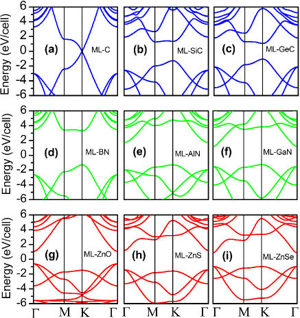
The LDA band structures of graphene (ML-C)
and some other mono-layers of SiC, GeC, BN,
AlN, GaN, ZnO, ZnS and ZnSe in graphene-like
planar structure are depicted in Figure 5 and in
Table 3, we have listed our calculated LDA values
of the band gaps of these materials along with the
reported values. As seen in the explicit case of
ML-BN in Table 3, although LDA under-estimates
the band gap (in our case the calculated value is
about less than the experimental value of
5.971 eV) it correctly predicts the nature of the
gap. However, the use of a more advanced
approximation, such as the LDA + GW0 used in
[25], improves the band gap
problem (in the case of ML-BN although it
overestimates band gap by in this case), but
the authors of [25] have presented
their result in terms of an indirect band gap for
ML-BN as opposed to the experimental
observation of direct band gap in ref. [40].
In all other cases, the LDA nature of band
gap is the same as that of the LDA + GW0 band
gap. The important point is that the actual band
gap is always more than the LDA value.
In Table 4, we present our calculated values of the
effective masses of the charge carriers in ML-C,
ML-Si, ML-Ge, ML-BN, ML-AlN, ML-GaN, ZnO,
ZnS, ZnSe, determined at the band edges at the
special points as appropriate for the material under
study. From the linear energy dispersion close to the
point of the hexagonal Brillouin Zone (BZ) as
shown in Figure 6, mass-less carriers in graphene
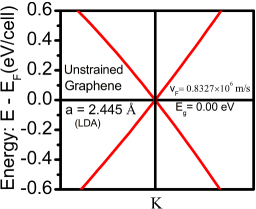
were inferred. As seen in Figure 6, near the point of the BZ,
the energy bad dispersion is linear in :
| (1) |
where is the magnitude of Fermi velocity of the charge carriers in graphene and is the magnitude of the momentum. Thus, charge carriers in graphene behave like mass-less relativistic particles. From the slope of the linear bands one obtains the value of , which in our calculation corresponds to m/s. This value of is close to the experimentally measured value of m/s in graphene monolayer deposited on graphite substrate [41] and the reported calculated LAPW value of m/s [42] and about less than that measured in coupled multi-layers [43, 44] and the tight-binding value: m/s [15]. The smallness in the value of in ref. [41] was attributed to the electron-phonon interactions due to strong coupling with the graphite substrate. However, the closeness of our calculated value of for a freestanding graphene monolayer with the results of ref. [41] suggests a very weak coupling of graphene to the graphite substrate used in ref. [41]. Surprisingly, our calculated value of is close to the measured value of m/s [45] in metallic single-walled carbon nanotube.
4 Conclusions
Using full potential DFT calculations we have investigated the structural and electronic properties of graphene and some other graphene-like materials. While our results corroborate the previous theoretical studies based on different methods, our calculations on ML-ZnSe, the two-dimensional bulk modulus of ML-GeC, ML-AlN, ML-GaN, MLZnO, ML-ZnS, and the effective masses of the binary monolayer compounds considered here are our new results. We hope, with the advancement of fabrication techniques, the hypothetical graphenelike materials discussed here will be synthesized in the near future for potential applications in a variety of novel nano-devices.
References
- [1] Novoselov K.S., Geim A.K., Morozov S.V., Jiang D., Zhang Y., Dubono S.V., Grigorieva, I.V. and Firsov A.A., 2004. Electric field effect in atomically thin carbon films. Science 306, 666-669.
- [2] Novoselov K.S., Geim A. K., Morozov S.V., Jiang D., Zhang Y., Dubonos S. V. and Firsov A. A., 2005. Twodimensional gas of massless dirac fermions in graphene. Nature 438, 197-200.
- [3] Novoselov K.S., Jiang D., Schedin F., Booth T., Khotkevich V. V., Morozov S. V., Geim A. K., 2005, Twodimensional atomic crystals. Proc. Natl. Acad. Sci. USA. 102, 51-53.
- [4] Zhang Y., Tan Y-W., Stormer H. L. and Kim P., 2005. Experimental observation of the quantum hall effect and berry s phase in graphene. Nature 438, 201-204.
- [5] Brodie B.C., 1859. On the atomic weight of graphite. Phil. Trans. R. Soc. Lond. 149, 249-259.
- [6] Geim A. K., 2011. Nobel Lecture: Random walk to graphene. Rev. Mod. Phys. 83, 851-862.
- [7] Novoselov K.S., 2011. Nobel lecture: Graphene: materials in the flatland. Rev. Mod. Phys. 83, 837-849.
- [8] Geim A. K., 2012. Graphene prehistory. Phys. Scr. T146, 014003-014007.
- [9] Boehm H.P., Setton R. and Stumpp E., 1986. Nomenclature and terminology of graphite intercalation compounds. Carbon 4, 241-245.
- [10] Peierls R., 1935. Quelques proprieties typiques descorpses solides. Ann. Inst. Henri Poincare 3, 177-222.
- [11] Landau L.D., 1937. Zur theorie der phasenumwandlungen II. Phys. Z. Sowjetunion 11, 26-35.
- [12] Mermin N.D.,1968, Crystalline order in two dmension. Phys. Rev. 176, 250-254.
- [13] Meyer J.C., Geim A.K., Katsnelson M.I., Novoselov K.S., Booth T.J. and Roth S., 2007. The structure of suspended graphene sheets. Nature 446, 60-63.
- [14] Geim A. K. and Novoselov K.S., 2007. The rise of graphene. Nature Mater. 6, 183-191.
- [15] Castro Neto A.H., Guinea F., Peres N.M.R., Novoselov K.S. and Geim A.K., 2009. The electronic properties of graphene. Rev. Mod. Phys. 81, 109-162.
- [16] Geim A. K., 2009. Graphene: Status and prospects. Science 324, 1530-1534.
- [17] Abergel D.S.L., Apalkov V., Berashevich J., Ziegler K. and Chakraborty T., 2010. Properties of graphene: a theoretical perspective. Adv. in Phys. 59, 261-482.
- [18] Singh V., Joung D., Zhai L., Das S., Khondaker S. I. and Seal S., 2011. Graphene based materials: Past, present and future. Prog. in Mater. Sci. 56, 1178-1271.
- [19] Castro Neto A.H. and Novoselov K., 2011. New directions in science and technology: two-dimensional crystals. Rep. Prog. Phys. 74, 1-9.
- [20] Novoselov K.S., Jiang D., Schedin F., Booth T., Khotkevich V. V., Morozov S. V., Geim A. K., 2005b, Twodimensional atomic crystals. Proc. Natl. Acad. Sci. USA. 102, 51-53.
- [21] Castro Neto A.H. and Novoselov K., 2011. New directions in science and technology: two-dimensional crystals. Rep. Prog. Phys. 74, 1-9.
- [22] Kara A., Enriquez H., Seitsonen A.P., Lew Yan Voon L.C. and Vizzini S., 2012. A review on silicene-new candidate for electronics. Surf. Sci. Rep. 67, 1-18.
- [23] Tusche C., Meyerheim H. L. and Kirshner J., 2007. Observation of depolarized ZnO(0001) monolayers: Formation of unreconstructed planar sheets. Phys. Rev. Lett. 99, 026102 (4 pp).
- [24] Freeman C.L., Claeyssens F., AllanN. L. and Harding J. H., 2006. Graphitic nanofilms as precursors to wurtzite films: Theory. Phys. Rev. Lett. 96, 066102 (4 pp).
- [25] Şahin H., Cahangirov S., Topsakal M., Bekaroglu E., Aktürk E., Senger R.T. and Ciraci S., 2009. Monolayer honeycomb structures of group-IV and III-V binary compounds: First-principles calculations. Phys. Rev. B 80, 155453 (12 pp).
- [26] Wang S., 2010. Studies of physical properties of twodimensional hexagonal crystals by first-principles calculations. J. Phys. Soc. Jpn 79(6), 064602-064607.
- [27] Sjöstedt E., Nordström L. and Singh D. J., 2000. An alternative way of linearizing the augmented plane- wave method. Solid State Commun. 114, 15-20.
- [28] Madsen G.K.H., Blaha P., Schwarz K., Sjöstedt E. and Nordström L., 2001. Efficient linearization of the augmented plane-wave method. Phys. Rev. B 64, 195134 (9 pp).
- [29] Singh D. J. and Nordström L., 2006. Planewaves, pseudopotentials, and the LAPW method (Springer, N.Y.).
- [30] Perdew P. and Zunger A., 1981. Self-interation correction to density-functional approximations for many electron systems. Phys. Rev. B 23, 5048-5079.
- [31] Behera H. and Mukhopadhyay G., 2010. Structural and electronic properties of graphene and silicene: An FP-(L)APW+lo Study. AIP Conf. Proc. 1313, 152-155. http://arxiv.org/abs/1111.1282
- [32] Behera H. and Mukhopadhyay G., 2011. First-principles study of structural and electronic properties of germanene. AIP Conf. Proc. 1349, 823-824. http://arxiv.org/abs/1111.6333
- [33] Behera H. and Mukhopadhyay G., 2012. Strain-tunable band gap in graphene/h-BN hetero-bilayer. J. Phys.Chem. Solids 73, 818-821. http://arxiv.org/abs/1204.2030
- [34] Behera H. and Mukhopadhyay G., 2012. Strain-tunable bandgaps of two-dimensional hexagonal BN and AlN: An FP-(L)APW+lo study. AIP Conf. Proc. 1447, 273-274. http://arxiv.org/abs/1206.3162
- [35] Behera H. and Mukhopadhyay G., 2012. Strain-tunable direct band gap of ZnO monolayer in graphene-like honeycomb structure. Phys. Lett. A. 376, 3287-3289. http://arxiv.org/abs/1211.3034
- [36] Behera H. and Mukhopadhyay G., 2012. Strain-tunable band gap of a monolayer graphene analogue of ZnS monolayer. Presented in the International Conference on Composites/Nano-Engineering, Beijing, China. http://arxiv.org/abs/1210.3309
- [37] Mukhopadhyay G. and Behera H., 2012, Structural and electronic properties of graphene and graphene-like materials. Presented in the International Conference on Composites/Nano-Engineering, Beijing, China.
- [38] Monkhorst H.J. and Pack J.D., 1976. Special points for Brillouin-zone integrations. Phys. Rev. B 13, 5188-5192.
- [39] Perdew J. P., Burke K. and Wang Y., 1996. Generalized gradient approximation for the exchange-correlation hole of a many-electron system. Phys. Rev. B 54, 16533-16539.
- [40] Watanabe K., Taniguchi T. and Kanda H., 2004. Direct bandgap properties and evidence for ultraviolet lasing of hexagonal boron nitride single crystal. Nature Mater 3, 404-409.
- [41] Li G., Luican A. and Andrei E.Y., 2009. Scanning tunneling spectroscopy of graphene on graphite. Phys. Rev. Lett. 102, 176804 (4 pp).
- [42] Gmitra M., Konschuh S., Ertler C., Ambrosch-Draxl C. and Fabian J., 2009. Band-structure topologies of graphene: Spin-orbit coupling effects from first principles, Phys. Rev. B 80, 235431 (5 pp).
- [43] Li G. and Andrei E.Y., 2007. Observation of landau levels of dirac fermions in graphite. Nature Phys. 3, 623-627.
- [44] Miller D.L., Kubista K.D., Rutter G. M., Ruan M., der Heer W. A., First P. N. and Stroscio A., 2009. Observing the quantization of zero mass carriers in graphene. Science 324, 924-927.
- [45] Liang W., Bockrath Marc, Bozovic D., Hafner J.H., Tinkham M. and Park Hongkun, 2001. Fabryperot interference in a nanotube electron waveguide. Nature 411, 665-669.
- [46] Topsakal M., Cahangirov S., Bekaroglu E. and Ciraci S., 2009. First-principles study of zinc oxide honeycomb structures. Phys. Rev. B 80, 235119 (14 pp).
- [47] Krainara N., Limtrakul J., Illas F. and Bromley S.T., 2011. Structural and electronic bistability in ZnS single sheets and single-walled nanotubes. Phys. Rev. B 83, 233305 (4 pp).
- [48] Dzade N.Y., Obodo K.O., Adjokatse S.K., Ashu A.C., Amankwah E., Atiso C.D., Bello A.A., Igumbor E., Nzabarinda S.B., Obodo J.T., Ogbuu A.O., Femi O. E., Udeigwe J.O. and Waghmare U.V., 2010. Silicene and transition metal based materials: prediction of a twodimensional piezomagnet. J. Phys.: Condens. Mater. 22, 375-502.
- [49] Michel K.H. and Verberck B., 2009. Theory of elastic and piezoelectric effects in two-dimensional hexagonal boron nitride. Phys. Rev. B 80, 224301 (10 pp).