Transient Charge and Energy Balance in Graphene Induced by Ultrafast Photoexcitation

Junhua Zhang,1 JoΒ¨Β¨π‘œ\ddot{o}rg Schmalian,2 Tianqi Li,3 and Jigang Wang3 1Department of Physics, College of William and Mary, Williamsburg, Virginia 23187, USA
2Institute for Theory of Condensed Matter and Center for Functional Nanostructures, Karlsruhe Institute of Technology, Karlsruhe 76128, Germany
3Ames Lab and Department of Physics and Astronomy, Iowa State University, Ames, Iowa 50011, USA
Abstract

Ultrafast optical pump-probe spectroscopy measurement on monolayer graphene observes significant optical nonlinearities. We show that strongly photoexcited graphene monolayers with 353535fs pulses quasi-instantaneously build up a broadband, inverted Dirac fermion population. Optical gain emerges and directly manifests itself via a negative conductivity at the near-infrared region for the first 200fs, where stimulated emission completely compensates absorption loss in the graphene layer. To quantitatively investigate this transient, extremely dense photoexcited Dirac-fermion state, we construct a two-chemical-potential model, in addition to a time-dependent transient carrier temperature above lattice temperature, to describe the population inverted electronic state metastable on the time scale of tens of femtoseconds generated by a strong exciting pulse. The calculated transient optical conductivity reveals a complete bleaching of absorption, which sets the saturation density during the pulse propagation. Particularly, the model calculation reproduces the negative optical conductivity at lower frequencies in the states close to saturation, corroborating the observed femtosecond stimulated emission and optical gain in the wide near-infrared window.

1 Introduction

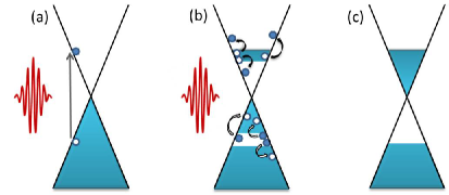
Despite the well-established linear optical properties in graphene, which is marked by a universal absorption A=π​α=2.3%π΄πœ‹π›Όpercent2.3A=\pi\alpha=2.3\% ranging from near-infrared to visible light,[1, 2, 3] significantly less attention has been paid to the ultrafast nonlinear optical properties. Important for future photonic and optoelectronic applications,[4] carrier dynamics in graphene after being driven far out of equilibrium needs to be understood. Still, ultrafast spectroscopy studies are reported recently to show unusual properties.[5, 6, 7, 8, 9, 10, 11, 12, 13, 14, 15, 16, 17, 18, 19, 20, 21] Especially, the observation of nonlinear absorption when applying an ultrashort intense laser pulse to monolayer graphene reveals an extremely dense, quasithermal photoexcited-carrier state created by strong pumping on 10 fs time scale and metastable for several tens of femtoseconds, which implies a unique transient electronic state in the important emerging material graphene.[18]

When strongly driven out of equilibrium by coherent light, the excited carriers subsequently participate in several dynamical processes during relaxing back to its equilibrium. Among them are the carrier decoherence, thermalization, cooling, and electron-hole recombination. If the excitation pulse is short enough, by observing the responses followed from right after the pump, we can identify the typical time scales associated with theses processes. Facilitated by recent ultrafast spectroscopy measurements, certain progress has been made. It is recognized that the ultrafast carrier dynamics in graphene is different from that in metals and semiconductors. First of all, dimensional estimates for Dirac fermions in graphene yield the carrier decoherence time Ο„dcβˆ’1∼e4(ℏ​v)2​ℏ​ωsimilar-tosuperscriptsubscript𝜏dc1superscript𝑒4superscriptPlanck-constant-over-2-pi𝑣2Planck-constant-over-2-piπœ”\tau_{\text{dc}}^{-1}\sim\frac{e^{4}}{(\hbar v)^{2}}\hbar\omega,[22] which becomes rather short, Ο„dc∼1​fssimilar-tosubscript𝜏dc1fs\tau_{\text{dc}}\sim 1\text{fs}, for pump photon energy on the order of 1eV. Rapid carrier-carrier scattering gives rise to an electronic thermalization time Ο„thsubscript𝜏th\tau_{\text{th}} on the order of 10 fs.[12, 18] Time-resolved studies observe different cooling time scales with the shortest Ο„c∼100​fssimilar-tosubscript𝜏c100fs\tau_{\text{c}}\sim 100\text{fs} from electron-optical phonon coupling and longer electron-hole recombination time Ο„rsubscript𝜏r\tau_{\text{r}} on the ps time scale.[5, 11, 10, 6, 12, 13, 23, 24, 25] Thus, when applying an ultrashort pump pulse of Ο„p∼10​fssimilar-tosubscript𝜏p10fs\tau_{\text{p}}\sim 10\text{fs}, the distinct time scales Ο„thβ‰ͺΟ„c,rmuch-less-thansubscript𝜏thsubscript𝜏c,r\tau_{\text{th}}\ll\tau_{\text{c,r}} entails an intermediate electronic state purely determined by carrier-carrier scattering. Unlike in most semiconductors where Ο„th∼100​fs>Ο„psimilar-tosubscript𝜏th100fssubscript𝜏p\tau_{\text{th}}\sim 100\text{fs}>\tau_{\text{p}}, the extremely short decoherence time and the rapid carrier-carrier scattering quickly deplete the phase space from the neighbourhood of optical excitation to the whole band to fully thermalize the carriers as illustrated in Fig. 1 (b). The analysis of Coulomb interaction between the Dirac-fermionic excitations shows a slow population imbalance relaxation,[22, 26] in particular at high pulse intensity due to the suppression of Auger processes for strong pulse excitation,[25] although there is no gap. Thus for Ο„th<t<Ο„c,rsubscript𝜏th𝑑subscript𝜏c,r\tau_{\text{th}}<t<\tau_{\text{c,r}} the number of photoexcited carriers in each branch of the Dirac cone decays rather slowly. Therefore, the fast decoherence and thermalization together with slow imbalance relaxation support a unique population-inverted electronic state adiabatically formed after the strong pump excitation, a quasi-stable β€œhourglass” state on the time scale of some tens of femtoseconds, as shown in Fig. 1 (c).

Refer to caption
Figure 1: Schematic illustration of the formation of population inverted electronic state in the intermediate time Ο„th<t<Ο„c,rsubscript𝜏th𝑑subscript𝜏c,r\tau_{\text{th}}<t<\tau_{\text{c,r}}. (a) Photoexcited carriers generated by ∼similar-to\sim10fs pump pulse; (b) The leading scattering processes of photo-excited carriers taking place in several femtoseconds: e+eβ†’e+e,h+hβ†’h+h,e+hβ†’e+hformulae-sequence→𝑒𝑒𝑒𝑒formulae-sequenceβ†’β„Žβ„Žβ„Žβ„Žβ†’π‘’β„Žπ‘’β„Že+e\rightarrow e+e,\ h+h\rightarrow h+h,\ e+h\rightarrow e+h, which quickly establish individual thermalization in electron and hole carriers sharing a common electronic temperature Tesubscript𝑇𝑒T_{e} due to the electron-hole scattering events. (c) After the internal thermalization, the photoexcited carriers form a population inverted hourglass-like electronic state characterized by two chemical potentials and a common electron temperature.

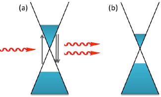
In this article, we focus on this unique transient electronic state and provide details on ultrafast optical pump-probe spectroscopy measurement on monolayer graphene to reveal significant ultrafast optical nonlinearities, including nonlinear absorption saturation and near-infrared stimulated emission. These properties arise from a broadband, inverted Dirac fermion population induced by 353535fs pulse excitation. Optical gain emerges and directly manifests itself via a negative conductivity at the near-infrared region for the first 100s of fs, where stimulated emission completely compensates absorption loss in the graphene layer. To quantitatively investigate this transient, extremely dense photoexcited Dirac-fermion state, we construct a simple model of a quasi-thermalized distribution with one electron temperature but two distinct chemical potentials associated with the electron- and hole-band, respectively. We find this transient state associated with high electron temperature Tesubscript𝑇𝑒T_{e} up to 3000-4000K, which causes a broadband distribution extending to high energy that naturally explains the observed blueshifted component in photoluminescence spectrum.[7, 8, 9] We further explore the phase space capacity and identify the maximal photoexcitation density restricted by phase space filling. and individual chemical potential of each band are calculated. To understand the observed nonlinear optical behavior and the measured large saturation density, we calculate the optical conductivity for this nonequilibrium electronic state. The results show that the available phase space cannot be completely filled but will be saturated at a lower photoexcitation density due to the balance between absorption and emission. This calculated saturation density is in excellent agreement with the experimental value.[18] Most interestingly, our model reproduces the experimental results that the nearly-saturated states created by a high-frequency pump are unstable to a low-frequency pulse through stimulated emission to bring the system to a lower-level metastable state (illustrated in Fig. 2), resulting in an optical gain phenomenon within the first 100s of fs after photoexcitation. The excellent agreement between theory and experiment further corroborates that our simple model captures the feature of the transient state at early timescale (<100​fsabsent100fs<100\text{fs}) in the high excitation regime. Meanwhile, the comparison with the measured optical conductivity disfavors the equal-chemical-potential model to describe the transient states in graphene at the fs time scale, an outstanding issue debated in the community.

Refer to caption
Figure 2: Schematic illustration of (a) the femtosecond stimulated emission and optical gain when applying a low-frequency pulse to a high-density population-inverted state created by an intense high-frequency pump and (b) the resulting metastable low-density state.

2 Experimental Details

2.1 Spectroscopy measurement

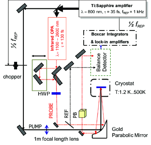
The experimental setup is shown in Fig. 3. In our experiment, the Ti:Sapphire amplifier with center wavelength 800nm, pulse width 35fs at 1kHz repetition rate is used. This further drives an optical parametric amplifiers tunable with tunable optical pump pulses covering 572-2400 nm allowing for both degenerate and non-degenerate pump/probe spectroscopy. The laser is further split into pump and probe paths. The pump beam, chopped as half harmonic of the laser repetition rate, directly excites the sample. The reflection of the probe beam, together with reference, is fed into an auto-balance detector, and the individual beams as well as the difference between them are picked up by three boxcar integrators. During the measurement, the pump fluence from few ΞΌπœ‡\muJ/c​m2absent𝑐superscriptπ‘š2/cm^{2} to mπ‘šmJ/c​m2absent𝑐superscriptπ‘š2/cm^{2} level is finely controlled. This way we can record pump-induced differential reflectivity changes Δ​R/RΔ𝑅𝑅\Delta R/R with ∼similar-to\sim40fs time resolution and signal-to-noise ratio down to 5β‹…β‹…\cdot10-5. Similar experimental setups and details are described elsewhere, e.g., see Refs. [27, 28, 29, 30, 31, 32].

Refer to caption
Figure 3: Experimental Schematics. HWP: half waveplate; PB: polarizing beam splitter, FL: focal length.

2.2 Samples

Graphene was prepared from the thermal evaporation of SiC [33] with substrates used in the current experiments 6H-SiC(0001) purchased from Cree, Inc.. The samples were graphitized in UHV (P∼1Γ—10βˆ’10similar-toP1superscript1010\mathrm{P}\sim 1\times 10^{-10}torr) by direct current heating of the sample to ∼similar-to\sim1300Β°C measured with an infrared pyrometer with reading of the pyrometer adjusted to take account of the graphite emissivity reported in the literature [34]. The sample was not pretreated in a H2 atmosphere within a furnace which is a common practice because it excludes the formation of multi-step heights and easier control of thickness. The layer thickness (whether single layer G1 or bilayer G2) was controlled by the heating rate: faster one-step heating rates (within 2-3 seconds to reach 1300Β°C) result in large G1 domains while multiple heating steps with a slower rate (30seconds to reach 1350Β°C) result in samples with large G2 areas. Graphene thickness was identified using contrast thickness [35] and with step heights changes between different regions which were found to be combinations of only two steps ,i.e., 0.25nm (of SiC), and 0.33nm (of graphene ) as explained in Ref.[33]. Fig. 1c in Ref. [18] shows a large 2​μ​mΓ—2​μ​m2πœ‡m2πœ‡m2\mu\mathrm{m}\times 2\mu\mathrm{m} (left) G1 formed after heating with the fast rate. The atomic scale image is shown to the right with the 1Γ—1111\times 1 unit cell seen with lattice constant 0.246nm and intensity modulation due to the 6​3636\sqrt{3} is also seen. The tunneling conditions are -0.5V, 1nA. The high intensity of the modulation and the resolution of the 6 atoms of the graphene ring indicate that this is predominantly G1(in excess of 90% of the area). The detailed growth conditions, characterizations and doping (∼similar-to\sim0.4 eV for monolayer) of the obtained epitaxial graphene on SiC are extensively established by our papers [33, 36] and many others in the literature, e.g., [37, 38, 39].

3 Threshold reflection coefficient and optical gain

Considering graphene on a substrate with dielectric constant Ξ΅ssubscriptπœ€π‘ \varepsilon_{s}, the amplitude of the reflected and transmitted waves for a normal incident beam follow from Maxwell’s equations along with the usual boundary conditions:

r^^π‘Ÿ\displaystyle\hat{r} =\displaystyle= 1βˆ’nsβˆ’4​π​σ​(Ο‰)/c1+ns+4​π​σ​(Ο‰)/c,1subscript𝑛𝑠4πœ‹πœŽπœ”π‘1subscript𝑛𝑠4πœ‹πœŽπœ”π‘\displaystyle\frac{1-n_{s}-4\pi\sigma\left(\omega\right)/c}{1+n_{s}+4\pi\sigma\left(\omega\right)/c},
t^^𝑑\displaystyle\hat{t} =\displaystyle= 21+ns+4​π​σ​(Ο‰)/c.21subscript𝑛𝑠4πœ‹πœŽπœ”π‘\displaystyle\frac{2}{1+n_{s}+4\pi\sigma\left(\omega\right)/c}. (1)

Here σ​(Ο‰)πœŽπœ”\sigma\left(\omega\right) is the complex optical conductivity. The common reflection and transmission coefficients are determined by R=|r^|2𝑅superscript^π‘Ÿ2R=\left|\hat{r}\right|^{2} and T=ns​|t^|2𝑇subscript𝑛𝑠superscript^𝑑2T=n_{s}\left|\hat{t}\right|^{2}. In case Οƒ=0𝜎0\sigma=0 holds that R+T=1𝑅𝑇1R+T=1. The presence of a finite conductivity in the graphene sheet leads to absorption

Ag=14​(1+ns)2​(1βˆ’Tβˆ’R).subscript𝐴𝑔14superscript1subscript𝑛𝑠21𝑇𝑅A_{g}=\frac{1}{4}\left(1+n_{s}\right)^{2}\left(1-T-R\right). (2)

where it is custom[40] to introduce the coefficient (1+ns)2/4superscript1subscript𝑛𝑠24\left(1+n_{s}\right)^{2}/4 such that Agsubscript𝐴𝑔A_{g} corresponds to the absorption coefficient of a suspended graphene sheet.

Following Ref.[40] we can introduce the reflection of the substrate (for Οƒ=0𝜎0\sigma=0)

Rs=(1βˆ’ns1+ns)2subscript𝑅𝑠superscript1subscript𝑛𝑠1subscript𝑛𝑠2R_{s}=\left(\frac{1-n_{s}}{1+n_{s}}\right)^{2} (3)

and of the substrate with graphene Rs+gsubscript𝑅𝑠𝑔R_{s+g}

Rs+g=|1βˆ’nsβˆ’4​π​σ​(Ο‰)/c1+ns+4​π​σ​(Ο‰)/c|2.subscript𝑅𝑠𝑔superscript1subscript𝑛𝑠4πœ‹πœŽπœ”π‘1subscript𝑛𝑠4πœ‹πœŽπœ”π‘2R_{s+g}=\left|\frac{1-n_{s}-4\pi\sigma\left(\omega\right)/c}{1+n_{s}+4\pi\sigma\left(\omega\right)/c}\right|^{2}. (4)

For the complex optical conductivity of graphene in equilibrium and at T=0𝑇0T=0 it holds

Οƒe​q(Ο‰,T=0)=e24​ℏ(ΞΈ(Ο‰βˆ’2ΞΌ)βˆ’i2​πln(Ο‰+2β€‹ΞΌΟ‰βˆ’2​μ)2).\sigma_{eq}\left(\omega,T=0\right)=\frac{e^{2}}{4\hbar}\left(\theta\left(\omega-2\mu\right)-\frac{i}{2\pi}\ln\left(\frac{\omega+2\mu}{\omega-2\mu}\right)^{2}\right). (5)

Near the jump in the optical conductivity at Ο‰=2β€‹ΞΌπœ”2πœ‡\omega=2\mu, the imaginary part of the conductivity has a logarithmic divergence which is smeared out in case of finite temperatures. Since σ​(Ο‰)πœŽπœ”\sigma\left(\omega\right) is of order e2/ℏsuperscript𝑒2Planck-constant-over-2-pie^{2}/\hbar, it holds that σ​(Ο‰)/cπœŽπœ”π‘\sigma\left(\omega\right)/c is of order of the finestructure constant of quantum electrodynamics Ξ±QED=e2/(ℏ​c)β‰ˆ1/137β‰ͺ1subscript𝛼QEDsuperscript𝑒2Planck-constant-over-2-pi𝑐1137much-less-than1\alpha_{\mathrm{QED}}=e^{2}/\left(\hbar c\right)\approx 1/137\ll 1. This allows for an expansion in σ​(Ο‰)/cπœŽπœ”π‘\sigma\left(\omega\right)/c. It follows

Rs+gβˆ’RsRs=4ns2βˆ’1​4​πc​σ′​(Ο‰)+O​(Ξ±QED2)subscript𝑅𝑠𝑔subscript𝑅𝑠subscript𝑅𝑠4superscriptsubscript𝑛𝑠214πœ‹π‘superscriptπœŽβ€²πœ”π‘‚superscriptsubscript𝛼QED2\frac{R_{s+g}-R_{s}}{R_{s}}=\frac{4}{n_{s}^{2}-1}\frac{4\pi}{c}\sigma^{\prime}\left(\omega\right)+O\left(\alpha_{\mathrm{QED}}^{2}\right) (6)

Thus, the reflection coefficient to leading order in Ξ±QEDsubscript𝛼QED\alpha_{\mathrm{QED}} is fully determined by the real part of the optical conductivity σ′​(Ο‰)=Re​σ​(Ο‰)superscriptπœŽβ€²πœ”ReπœŽπœ”\sigma^{\prime}\left(\omega\right)=\mathrm{Re}\sigma\left(\omega\right), the imaginary part only enters at higher orders. For the transmission and absorption coefficients follows in the same limit

T𝑇\displaystyle T =\displaystyle= 4​ns(1+ns)2βˆ’8​ns(ns+1)3​4​πc​σ′​(Ο‰)+O​(Ξ±QED2)4subscript𝑛𝑠superscript1subscript𝑛𝑠28subscript𝑛𝑠superscriptsubscript𝑛𝑠134πœ‹π‘superscriptπœŽβ€²πœ”π‘‚superscriptsubscript𝛼QED2\displaystyle\frac{4n_{s}}{\left(1+n_{s}\right)^{2}}-\frac{8n_{s}}{\left(n_{s}+1\right)^{3}}\frac{4\pi}{c}\sigma^{\prime}\left(\omega\right)+O\left(\alpha_{\mathrm{QED}}^{2}\right)
Agsubscript𝐴𝑔\displaystyle A_{g} =\displaystyle= 4​πc​σ′​(Ο‰)+O​(Ξ±QED2).4πœ‹π‘superscriptπœŽβ€²πœ”π‘‚superscriptsubscript𝛼QED2\displaystyle\frac{4\pi}{c}\sigma^{\prime}\left(\omega\right)+O\left(\alpha_{\mathrm{QED}}^{2}\right). (7)

This yields the result

Rg+sβˆ’RsRs=4ns2βˆ’1​Agsubscript𝑅𝑔𝑠subscript𝑅𝑠subscript𝑅𝑠4superscriptsubscript𝑛𝑠21subscript𝐴𝑔\frac{R_{g+s}-R_{s}}{R_{s}}=\frac{4}{n_{s}^{2}-1}A_{g} (8)

of Ref.[40].

Eq.6 enables us to determine a threshold value for the reflectivity that corresponds to a negative optical conductivity and thus to a behavior with optical gain. From Eq.6 it follows for the reflection after delay time Ο„πœ\tau:

Δ​R/RΔ𝑅𝑅\displaystyle\Delta R/R ≑\displaystyle\equiv Rs+g​(Ο„)βˆ’Rs+g​(0)Rssubscriptπ‘…π‘ π‘”πœsubscript𝑅𝑠𝑔0subscript𝑅𝑠\displaystyle\frac{R_{s+g}\left(\tau\right)-R_{s+g}\left(0\right)}{R_{s}} (9)
=\displaystyle= 4ns2βˆ’1​4​πc​(σ′​(Ο„)βˆ’Οƒβ€²β€‹(0))4superscriptsubscript𝑛𝑠214πœ‹π‘superscriptπœŽβ€²πœsuperscriptπœŽβ€²0\displaystyle\frac{4}{n_{s}^{2}-1}\frac{4\pi}{c}\left(\sigma^{\prime}\left(\tau\right)-\sigma^{\prime}\left(0\right)\right)

Using the experimentally established value σ′​(0)=e2/(4​ℏ)superscriptπœŽβ€²0superscript𝑒24Planck-constant-over-2-pi\sigma^{\prime}\left(0\right)=e^{2}/\left(4\hbar\right) for the optical conductivity prior to the pulse, it follows that σ′​(Ο„)<0superscriptπœŽβ€²πœ0\sigma^{\prime}\left(\tau\right)<0 if Δ​R/R​<Δ​R/R|cΔ𝑅𝑅subscriptbraΔ𝑅𝑅𝑐\Delta R/R<\left.\Delta R/R\right|_{c} where

Δ​R/R|c=βˆ’4​π​αQEDns2βˆ’1.evaluated-atΔ𝑅𝑅𝑐4πœ‹subscript𝛼QEDsuperscriptsubscript𝑛𝑠21\left.\Delta R/R\right|_{c}=-\frac{4\pi\alpha_{\mathrm{QED}}}{n_{s}^{2}-1}. (10)

With ns=2.7subscript𝑛𝑠2.7n_{s}=2.7 it follows Δ​R/R|c=βˆ’1.4582%.evaluated-atΔ𝑅𝑅𝑐percent1.4582\left.\Delta R/R\right|_{c}=-1.4582\%. If for some reason the dielectric constant of the substrate is larger that 2.72.72.7, this would only reduce the critical value of Δ​R/RΔ𝑅𝑅\Delta R/R and we would only underestimate the regime where Οƒ<0𝜎0\sigma<0. Given that our data yield the magnitude of Δ​R/RΔ𝑅𝑅\Delta R/R as big as 1.9%percent1.91.9\%, it follows that we have Οƒ<0𝜎0\sigma<0 as long as ns>2.41subscript𝑛𝑠2.41n_{s}>2.41. In the literature, the uncertainty of ns=2.7subscript𝑛𝑠2.7n_{s}=2.7 is Β±0.1plus-or-minus0.1\pm 0.1. The smallest index of SiC is 2.552.552.55 in the THz range. These results demonstrate that our conclusion Οƒ<0𝜎0\sigma<0 is robust.

In Fig. 4, we experimentally determine the existence and value of the threshold Δ​R/R|c=βˆ’1.4582%evaluated-atΔ𝑅𝑅𝑐percent1.4582\left.\Delta R/R\right|_{c}=-1.4582\% for zero conductivity in our sample. This further demonstrates unambiguously that the reflectivity geometry in current sample provides a direct measurement of the real part of conductivity ΟƒπœŽ\sigma of the graphene layer (or absorption), which directly accessing the gain/loss processes. This also demonstrates again our sample is graphene monolayer, consistent with conclusion from STM.

Refer to caption
Figure 4: The differential reflectivity determined by the measurements with Rg+s or without Rs graphene monolayer on SiC substrate. The reflection from the zero conductivity in pumped garphene/SiC exactly corresponds to the case of bare SiC substrate. Consequently, the threshold Δ​R/R|cevaluated-atΔ𝑅𝑅𝑐\left.\Delta R/R\right|_{c} for zero conductivity can be directly determined from the curve, which is consistent with value used in the manuscript ∼similar-to\sim-1.46%percent\%.

Using the same reasoning we can relate the reflectivity to the absorption coefficient

Rs+g​(Ο„)=Rs+nsβˆ’1ns+1​4(1+ns)2​A​(Ο„)subscriptπ‘…π‘ π‘”πœsubscript𝑅𝑠subscript𝑛𝑠1subscript𝑛𝑠14superscript1subscript𝑛𝑠2𝐴𝜏R_{s+g}\left(\tau\right)=R_{s}+\frac{n_{s}-1}{n_{s}+1}\frac{4}{\left(1+n_{s}\right)^{2}}A\left(\tau\right) (11)

and obtain

Ag​(Ο„)βˆ’Ag,0Ag,0=Rs+g​(Ο„)βˆ’Rs+g​(0)Rs+g​(0)β‹…ns2βˆ’1+4​Ag,04​Ag,0subscriptπ΄π‘”πœsubscript𝐴𝑔0subscript𝐴𝑔0β‹…subscriptπ‘…π‘ π‘”πœsubscript𝑅𝑠𝑔0subscript𝑅𝑠𝑔0superscriptsubscript𝑛𝑠214subscript𝐴𝑔04subscript𝐴𝑔0\frac{A_{g}\left(\tau\right)-A_{g,0}}{A_{g,0}}=\frac{R_{s+g}\left(\tau\right)-R_{s+g}\left(0\right)}{R_{s+g}\left(0\right)}\cdot\frac{n_{s}^{2}-1+4A_{g,0}}{4A_{g,0}} (12)

that will be used in our analysis of the density of transient electrons and holes, where Ag,0=Ag​(Ο„=0)=π​αQEDsubscript𝐴𝑔0subscriptπ΄π‘”πœ0πœ‹subscript𝛼QEDA_{g,0}=A_{g}\left(\tau=0\right)=\pi\alpha_{\mathrm{QED}}.

4 Stimulated infrared emission and optical gain

Refer to caption
Figure 5: (a) Ultrafast Δ​R/RΔ𝑅𝑅\Delta R/R at 1.55 eV pump and 1.33 eV probe for different pump fuences from 480 to 4759ΞΌπœ‡\muJ/c​m2absent𝑐superscriptπ‘š2/cm^{2}(b) Experimental values (rectangles) vs. theory (line) for peak transient conductivity, showing negative conductivity above a threshold pump fluence. (c) The extracted peak transient transmission as function of the pump fluence clearly shows the positive transmission change, nonlinear saturation, and that the critical vaule Δ​TT|cevaluated-atΔ𝑇𝑇𝑐\frac{\Delta T}{T}|_{c} (blue line) for zero conductivity indeed occurs.

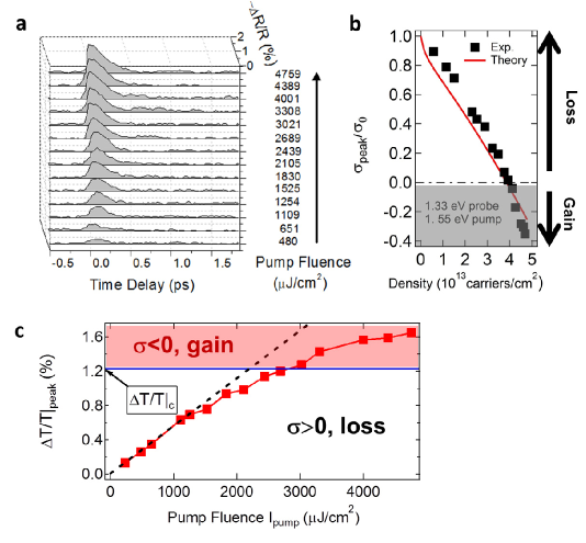
Here we provide a set of pump fluence dependence data at probe photon probe energy at 1.33 eV, as shown in Figs. 5a and 5b. Our conclusions w.r.t. stimulated emission and optical gain are based on the observed negative conductivity in strongly photoexcited graphene, which is fully consistent with the complementary data presented in Ref [18]. In addition, following the similar analysis Eqs. (6) and (7), the differential transmission of our sample can be extracted by the information of the differential reflectivity or the subsequently derived conductivity of the graphene sample. More importantly, there also exists a threshold value for the photoinduced differential transmission Δ​TT|cevaluated-atΔ𝑇𝑇𝑐\frac{\Delta T}{T}|_{c} that corresponds to a zero optical conductivity, above which the optical gain has to emerge because of the negative conductivity.

Δ​TT|c=2​π​αQ​E​Dns+1evaluated-atΔ𝑇𝑇𝑐2πœ‹subscript𝛼𝑄𝐸𝐷subscript𝑛𝑠1\frac{\Delta T}{T}|_{c}=\frac{2\pi\alpha_{QED}}{n_{s}+1} (13)

From Eq.6 and Eq.7 it follows for the differential transmission after delay time Ο„πœ\tau:

Δ​TT​(Ο„)=Δ​RR​(Ο„)β‹…1βˆ’ns2.Ξ”π‘‡π‘‡πœβ‹…Ξ”π‘…π‘…πœ1subscript𝑛𝑠2\frac{\Delta T}{T}(\tau)=\frac{\Delta R}{R}(\tau)\cdot\frac{1-n_{s}}{2}. (14)

The extracted peak transient transmission as function of the pump Fluence, as shown in Fig. 5c, clearly shows the positive transmission change and, mostly critically, that the critical value (blue line) for zero conductivity indeed occurs. While those data for the transmission were obtained indirectly, from our reflectivity measurements, a direct measurement of the transmission would be an important confirmation of our results ideally using large area free standing graphene monolayer samples.

5 Analysis of the density of transient electrons/holes

The amplitude of the time dependent absorption A𝐴A as function of pump fluence can be derived from the measured differential reflectivity by applying the Fresnel equations in thin film limit [40, 41]

Δ​A​(Ip)A0=Δ​Rg+s​(Ip)Rg+sβ‹…ns2βˆ’1+4​Ag,04​Ag,0,Δ𝐴subscript𝐼𝑝subscript𝐴0β‹…Ξ”subscript𝑅𝑔𝑠subscript𝐼𝑝subscript𝑅𝑔𝑠superscriptsubscript𝑛𝑠214subscript𝐴𝑔04subscript𝐴𝑔0\frac{\Delta A(I_{p})}{A_{0}}=\frac{\Delta R_{g+s}(I_{p})}{R_{g+s}}\cdot\frac{n_{s}^{2}-1+4A_{g,0}}{4A_{g,0}}, (15)

where Rg+ssubscript𝑅𝑔𝑠R_{g+s} and Δ​Rg+sΞ”subscript𝑅𝑔𝑠\Delta R_{g+s} are the static reflectivity and pump-induced reflectivity changes for the graphene monolayer (g) on the substrate (s) with index ns=2.7subscript𝑛𝑠2.7n_{s}=2.7. Ag,0subscript𝐴𝑔0A_{g,0} is the absorption of graphene monolayer without pump, which takes a universal value of Ag,0=π​e2ℏ​c≃0.023subscript𝐴𝑔0πœ‹superscript𝑒2Planck-constant-over-2-pi𝑐similar-to-or-equals0.023A_{g,0}=\pi\frac{e^{2}}{\hbar c}\simeq 0.023, as determined by the universal a.c. conductivity Οƒ0=e24​ℏsubscript𝜎0superscript𝑒24Planck-constant-over-2-pi\sigma_{0}=\frac{e^{2}}{4\hbar}. Here the Δ​A​(Ip)/A0Δ𝐴subscript𝐼𝑝subscript𝐴0\Delta A(I_{p})/A_{0} is the relative differential absorption of graphene on the substrate: A0=4(ns+1)2​Ag,0subscript𝐴04superscriptsubscript𝑛𝑠12subscript𝐴𝑔0A_{0}=\frac{4}{(n_{s}+1)^{2}}A_{g,0}, which yields Δ​AA0=Δ​AgAg,0Δ𝐴subscript𝐴0Ξ”subscript𝐴𝑔subscript𝐴𝑔0\frac{\Delta A}{A_{0}}=\frac{\Delta A_{g}}{A_{g,0}}. Therefore Eq.(15) follows from Eq.(12). The peak amplitude A​(Ip)=A0+Δ​A​(Ip)𝐴subscript𝐼𝑝subscript𝐴0Δ𝐴subscript𝐼𝑝A(I_{p})=A_{0}+\Delta A(I_{p}) gradually diminishes as increasing the pump fluence. From the measured transient saturation curve above, one can extract the density of photoexcited electrons(holes) in graphene after the propagation of a single laser pulse of 35 fs (Ο„psubscriptπœπ‘\tau_{p}) with pump fluence Ipsubscript𝐼𝑝I_{p}

nex​(Ip)=βˆ«βˆ’βˆžβˆžd​tΟ„p​nex​(t,Ip)=1β„β€‹Ο‰β€‹βˆ«βˆ’βˆžβˆžd​tΟ„p​I​(t,Ip)​A​(t),subscript𝑛exsubscript𝐼𝑝superscriptsubscriptd𝑑subscriptπœπ‘subscript𝑛ex𝑑subscript𝐼𝑝1Planck-constant-over-2-piπœ”superscriptsubscriptd𝑑subscriptπœπ‘πΌπ‘‘subscript𝐼𝑝𝐴𝑑n_{\text{ex}}(I_{p})=\int_{-\infty}^{\infty}\frac{\mathrm{d}t}{\tau_{p}}n_{\text{ex}}(t,I_{p})=\frac{1}{\hbar\omega}\int_{-\infty}^{\infty}\frac{\mathrm{d}t}{\tau_{p}}I(t,I_{p})A\left(t\right), (16)

where I​(t,Ip)𝐼𝑑subscript𝐼𝑝I(t,I_{p}) is the Gaussian pulse envelop I​(t,Ip)=Ip​4​ln⁑2π​exp⁑[βˆ’4​ln⁑2Ο„p2​t2]𝐼𝑑subscript𝐼𝑝subscript𝐼𝑝42πœ‹42superscriptsubscriptπœπ‘2superscript𝑑2I(t,I_{p})=I_{p}\sqrt{\frac{4\ln 2}{\pi}}\exp\left[\frac{-4\ln 2}{\tau_{p}^{2}}t^{2}\right], normalized such that the total pulse fluence is Ip=βˆ«βˆ’βˆžβˆžd​tΟ„p​I​(t,Ip)subscript𝐼𝑝superscriptsubscriptd𝑑subscriptπœπ‘πΌπ‘‘subscript𝐼𝑝I_{p}=\int_{-\infty}^{\infty}\frac{\mathrm{d}t}{\tau_{p}}I(t,I_{p}). Since A​(t)=A0+Δ​A​(t)=A0​(1+Δ​A​(t)A0)𝐴𝑑subscript𝐴0Δ𝐴𝑑subscript𝐴01Δ𝐴𝑑subscript𝐴0A(t)=A_{0}+\Delta A(t)=A_{0}(1+\frac{\Delta A(t)}{A_{0}}), we have

nex​(t,Ip)=I​(t,Ip)​A0ℏ​ω​(1+Δ​A​(t)A0).subscript𝑛ex𝑑subscript𝐼𝑝𝐼𝑑subscript𝐼𝑝subscript𝐴0Planck-constant-over-2-piπœ”1Δ𝐴𝑑subscript𝐴0n_{\text{ex}}(t,I_{p})=\frac{I(t,I_{p})A_{0}}{\hbar\omega}\left(1+\frac{\Delta A(t)}{A_{0}}\right). (17)

Applied to graphene where Ο„thβ‰ͺΟ„pmuch-less-thansubscript𝜏thsubscriptπœπ‘\tau_{\mathrm{th}}\ll\tau_{p}, A​(t)𝐴𝑑A\left(t\right) is determined by the adiabatic dependence of the absorption on the pump fluence with Ipartial​(t,Ip)=βˆ«βˆ’βˆžtd​tβ€²Ο„p​I​(tβ€²,Ip)subscript𝐼partial𝑑subscript𝐼𝑝superscriptsubscript𝑑dsuperscript𝑑′subscriptπœπ‘πΌsuperscript𝑑′subscript𝐼𝑝I_{\text{partial}}\left(t,I_{p}\right)=\int_{-\infty}^{t}\frac{\mathrm{d}t^{\prime}}{\tau_{p}}I(t^{\prime},I_{p}). Consequently, Eq.17 becomes

nex​(t,Ip)=I​(t,Ip)​A0ℏ​ω​(1+Δ​A​(Ipartial​(t,Ip))A0).subscript𝑛ex𝑑subscript𝐼𝑝𝐼𝑑subscript𝐼𝑝subscript𝐴0Planck-constant-over-2-piπœ”1Δ𝐴subscript𝐼partial𝑑subscript𝐼𝑝subscript𝐴0n_{\text{ex}}(t,I_{p})=\frac{I(t,I_{p})A_{0}}{\hbar\omega}\left(1+\frac{\Delta A\left(I_{\text{partial}}(t,I_{p})\right)}{A_{0}}\right). (18)

We determine A​(Ipartial)𝐴subscript𝐼partialA\left(I_{\text{partial}}\right) experimentally from the reflectivity data of Fig. 6a, combined with Eq.15, as discussed above. Finally, from Eqs. (15)-(18) we have
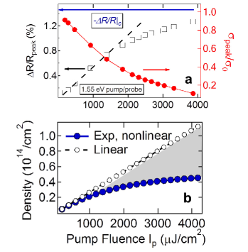
nex​(Ip)=βˆ«βˆ’βˆžβˆžI​(t,Ip)​A0ℏ​ω×[1+Δ​Rg+s​(Ipartial​(t,Ip))Rg+sβ‹…ns2βˆ’1+4​Ag,04​Ag,0]​d​tΟ„p.subscript𝑛exsubscript𝐼𝑝superscriptsubscript𝐼𝑑subscript𝐼𝑝subscript𝐴0Planck-constant-over-2-piπœ”delimited-[]1β‹…Ξ”subscript𝑅𝑔𝑠subscript𝐼partial𝑑subscript𝐼𝑝subscript𝑅𝑔𝑠superscriptsubscript𝑛𝑠214subscript𝐴𝑔04subscript𝐴𝑔0d𝑑subscriptπœπ‘n_{\text{ex}}(I_{p})=\int_{-\infty}^{\infty}\frac{I(t,I_{p})A_{0}}{\hbar\omega}\times\left[1+\frac{\Delta R_{g+s}\left(I_{\text{partial}}(t,I_{p})\right)}{R_{g+s}}\cdot\frac{n_{s}^{2}-1+4A_{g,0}}{4A_{g,0}}\right]\frac{\mathrm{d}t}{\tau_{p}}. (19)

The result is shown in Fig. 6b, which clearly shows that using the actual absorption A​(t)𝐴𝑑A\left(t\right), instead of A0subscript𝐴0A_{0}, is crutial to understand the high density regime of fs dynamics in graphene discussed here.

Refer to caption
Figure 6: (a) The peak △​RR|p​e​a​kevaluated-atβ–³π‘…π‘…π‘π‘’π‘Žπ‘˜{\frac{\triangle R}{R}}|_{peak} as function of the pump fluence (black squares) measured by degenerate differential reflectivity at 1.55 eV for the graphene monolayer and the corresponding conductivity change (red solid dots). Blue arrow marks the threshold for zero conductivity Δ​R/R|c=βˆ’1.4582%evaluated-atΔ𝑅𝑅𝑐percent1.4582\left.\Delta R/R\right|_{c}=-1.4582\% (see text). Dashed line: linear dependence (guide to the eyes). (b) The extracted transient fermion density at 40 fs (blue dots), as explained in the text, which is significantly lower than A0​Ip/ℏ​ωsubscript𝐴0subscript𝐼𝑝Planck-constant-over-2-piπœ”A_{0}I_{p}/\hbar\omega obtained from the universal conductivity (open circles), as illustrated in shadow area.

6 Theory

6.1 Model

We construct the theoretical model based on the following considerations: the above analysis of the time scales associated with different dynamical processes shows that the internal thermalization time Ο„thsubscript𝜏th\tau_{\text{th}} of the electron system is much shorter than the cooling Ο„csubscript𝜏c\tau_{\text{c}} and the electron-hole recombination time Ο„rsubscript𝜏r\tau_{\text{r}}; Simultaneous conservation of momentum and energy for Dirac-fermion scattering indicates the leading scattering processes are e+eβ†’e+e,h+hβ†’h+h,e+hβ†’e+hformulae-sequence→𝑒𝑒𝑒𝑒formulae-sequenceβ†’β„Žβ„Žβ„Žβ„Žβ†’π‘’β„Žπ‘’β„Že+e\rightarrow e+e,\ h+h\rightarrow h+h,\ e+h\rightarrow e+h in strong excitation regime with suppression of Auger processes.[25] For the intermediate time regime Ο„th<t<Ο„c,rsubscript𝜏th𝑑subscript𝜏c,r\tau_{\text{th}}<t<\tau_{\text{c,r}}, i.e., after absorbing photons but before losing energy to the lattice, photoexcited electrons and holes in graphene quickly establish separate thermal equilibrium through carrier-carrier scattering. This gives rise to sharply separated chemical potentials for the two bands, similar to the case of graphite thin film.[12] Due to the scattering between electron- and hole-carriers, e+hβ†’e+hβ†’π‘’β„Žπ‘’β„Že+h\rightarrow e+h, the whole electronic system obtains a common temperature, the electron temperature that differs from the lattice temperature. Therefore we characterize this intermediate electronic state by two Fermi-Dirac distributions

f±​(k)=1exp⁑[Ρ±​(k)βˆ’ΞΌΒ±kB​Te]+1subscript𝑓plus-or-minusπ‘˜1subscriptπœ€plus-or-minusπ‘˜subscriptπœ‡plus-or-minussubscriptπ‘˜Bsubscript𝑇𝑒1f_{\pm}(k)=\frac{1}{\exp\left[\frac{\varepsilon_{\pm}(k)-\mu_{\pm}}{k_{\text{B}}T_{e}}\right]+1} (20)

for the upper (++) and lower (βˆ’-) bands of the Dirac spectrum Ρ±​(k)=±ℏ​v​ksubscriptπœ€plus-or-minusπ‘˜plus-or-minusPlanck-constant-over-2-piπ‘£π‘˜\varepsilon_{\pm}(k)=\pm\hbar vk with separate chemical potential ΞΌΒ±subscriptπœ‡plus-or-minus\mu_{\pm} but the same electron temperature Tesubscript𝑇𝑒T_{e}. Note that for the convenience of theoretical calculation, we use the upper- and lower-band electron picture instead of the electron-hole picture, which are related via f+=fe,fβˆ’=1βˆ’fhformulae-sequencesubscript𝑓subscript𝑓𝑒subscript𝑓1subscriptπ‘“β„Žf_{+}=f_{e},\ f_{-}=1-f_{h} and ΞΌ+=ΞΌe,ΞΌβˆ’=βˆ’ΞΌhformulae-sequencesubscriptπœ‡subscriptπœ‡π‘’subscriptπœ‡subscriptπœ‡β„Ž\mu_{+}=\mu_{e},\ \mu_{-}=-\mu_{h}. To solve for electron temperature and chemical potentials, we take into account the following conservation laws: 1) the total number of electrons before and after pump excitation is the same, 2) a pseudo-conservation law due to the slow population imbalance relaxation valid in strong excitation regime: the photoexcited carrier number in the intermediate state stays the same as that of right after the pump excitation, 3) and the above described adiabatic process requires that the absorbed photon energy is kept in the electron system until the formation of the quasi-thermal distribution (20). These three conditions are expressed as

ntot=n++nβˆ’=n+0+nβˆ’0,subscript𝑛totsubscript𝑛subscript𝑛superscriptsubscript𝑛0superscriptsubscript𝑛0n_{\text{tot}}=n_{+}+n_{-}=n_{+}^{0}+n_{-}^{0}, (21)
nex=n+βˆ’n+0=nβˆ’0βˆ’nβˆ’,subscript𝑛exsubscript𝑛superscriptsubscript𝑛0superscriptsubscript𝑛0subscript𝑛n_{\text{ex}}=n_{+}-n_{+}^{0}=n_{-}^{0}-n_{-}, (22)
nex​ℏ​ω=uβˆ’u0,subscript𝑛exPlanck-constant-over-2-piπœ”π‘’superscript𝑒0n_{\text{ex}}\hbar\omega=u-u^{0}, (23)

where ntot=Ntot/L2subscript𝑛totsubscript𝑁totsuperscript𝐿2n_{\text{tot}}=N_{\text{tot}}/L^{2} represents the total density of electrons in the system, nex=Nex/L2subscript𝑛exsubscript𝑁exsuperscript𝐿2n_{\text{ex}}=N_{\text{ex}}/L^{2} refers to the density of photoexcited carriers, nΒ±subscript𝑛plus-or-minusn_{\pm} (nΒ±0superscriptsubscript𝑛plus-or-minus0n_{\pm}^{0}) indicate the electron densities in the intermediate (initially equilibrium) state, and u𝑒u (u0superscript𝑒0u^{0}) represents the intermediate (initial) energy density of the whole electron system while ℏ​ωPlanck-constant-over-2-piπœ”\hbar\omega is the pump photon energy. Applying the distribution (20) to Eqs. (21)-(23) and taking into account the valley and spin degeneracy in graphene, we obtain the following expressions in terms of fugacities z0=eΞΌ0kB​Te0,zΒ±=eΞΌΒ±kB​Teformulae-sequencesuperscript𝑧0superscript𝑒superscriptπœ‡0subscriptπ‘˜Bsuperscriptsubscript𝑇𝑒0subscript𝑧plus-or-minussuperscript𝑒subscriptπœ‡plus-or-minussubscriptπ‘˜Bsubscript𝑇𝑒z^{0}=e^{\frac{\mu^{0}}{k_{\text{B}}T_{e}^{0}}},\ z_{\pm}=e^{\frac{\mu_{\pm}}{k_{\text{B}}T_{e}}} with initial temperature Te0=300​Ksuperscriptsubscript𝑇𝑒0300KT_{e}^{0}=300\text{K},

δ𝛿\displaystyle\delta =\displaystyle= g2​π​(kB​Te)2(ℏ​v)2​[βˆ’Li2​(βˆ’z+)+Li2​(βˆ’1zβˆ’)]𝑔2πœ‹superscriptsubscriptπ‘˜Bsubscript𝑇𝑒2superscriptPlanck-constant-over-2-pi𝑣2delimited-[]subscriptLi2subscript𝑧subscriptLi21subscript𝑧\displaystyle\frac{g}{2\pi}\frac{(k_{\mathrm{B}}T_{e})^{2}}{(\hbar v)^{2}}\left[-\mathrm{Li}_{2}(-z_{+})+\mathrm{Li}_{2}\left(-\frac{1}{z_{-}}\right)\right] (24)
=\displaystyle= g2​π​(kB​Te0)2(ℏ​v)2​[βˆ’Li2​(βˆ’z0)+Li2​(βˆ’1z0)],𝑔2πœ‹superscriptsubscriptπ‘˜Bsuperscriptsubscript𝑇𝑒02superscriptPlanck-constant-over-2-pi𝑣2delimited-[]subscriptLi2superscript𝑧0subscriptLi21superscript𝑧0\displaystyle\frac{g}{2\pi}\frac{(k_{\mathrm{B}}T_{e}^{0})^{2}}{(\hbar v)^{2}}\left[-\mathrm{Li}_{2}(-z^{0})+\mathrm{Li}_{2}\left(-\frac{1}{z^{0}}\right)\right],

with δ𝛿\delta referring to the initial doping density with respect to the neutrality point, and

nexsubscript𝑛ex\displaystyle n_{\text{ex}} =\displaystyle= g2​π​1(ℏ​v)2​{(kB​Te)2​[βˆ’Li2​(βˆ’z+)]βˆ’(kB​Te0)2​[βˆ’Li2​(βˆ’z0)]}𝑔2πœ‹1superscriptPlanck-constant-over-2-pi𝑣2superscriptsubscriptπ‘˜Bsubscript𝑇𝑒2delimited-[]subscriptLi2subscript𝑧superscriptsubscriptπ‘˜Bsuperscriptsubscript𝑇𝑒02delimited-[]subscriptLi2superscript𝑧0\displaystyle\frac{g}{2\pi}\frac{1}{(\hbar v)^{2}}\left\{(k_{\mathrm{B}}T_{e})^{2}\left[-\mathrm{Li}_{2}(-z_{+})\right]-(k_{\mathrm{B}}T_{e}^{0})^{2}\left[-\mathrm{Li}_{2}(-z^{0})\right]\right\} (25)
=\displaystyle= g2​π​1(ℏ​v)2​{(kB​Te)2​[βˆ’Li2​(βˆ’1zβˆ’)]βˆ’(kB​Te0)2​[βˆ’Li2​(βˆ’1z0)]},𝑔2πœ‹1superscriptPlanck-constant-over-2-pi𝑣2superscriptsubscriptπ‘˜Bsubscript𝑇𝑒2delimited-[]subscriptLi21subscript𝑧superscriptsubscriptπ‘˜Bsuperscriptsubscript𝑇𝑒02delimited-[]subscriptLi21superscript𝑧0\displaystyle\frac{g}{2\pi}\frac{1}{(\hbar v)^{2}}\left\{(k_{\mathrm{B}}T_{e})^{2}\left[-\mathrm{Li}_{2}\left(-\frac{1}{z_{-}}\right)\right]-(k_{\mathrm{B}}T_{e}^{0})^{2}\left[-\mathrm{Li}_{2}\left(-\frac{1}{z^{0}}\right)\right]\right\},

as well as

nex​ℏ​ωsubscript𝑛exPlanck-constant-over-2-piπœ”\displaystyle n_{\text{ex}}\hbar\omega =\displaystyle= gπ​(kB​Te)3(ℏ​v)2​[βˆ’Li3​(βˆ’z+)βˆ’Li3​(βˆ’1zβˆ’)]π‘”πœ‹superscriptsubscriptπ‘˜Bsubscript𝑇𝑒3superscriptPlanck-constant-over-2-pi𝑣2delimited-[]subscriptLi3subscript𝑧subscriptLi31subscript𝑧\displaystyle\frac{g}{\pi}\frac{(k_{\mathrm{B}}T_{e})^{3}}{(\hbar v)^{2}}\left[-\mathrm{Li}_{3}\left(-z_{+}\right)-\mathrm{Li}_{3}\left(-\frac{1}{z_{-}}\right)\right] (26)
βˆ’gπ​(kB​Te0)3(ℏ​v)2​[βˆ’Li3​(βˆ’z0)βˆ’Li3​(βˆ’1z0)].π‘”πœ‹superscriptsubscriptπ‘˜Bsuperscriptsubscript𝑇𝑒03superscriptPlanck-constant-over-2-pi𝑣2delimited-[]subscriptLi3superscript𝑧0subscriptLi31superscript𝑧0\displaystyle-\frac{g}{\pi}\frac{(k_{\mathrm{B}}T_{e}^{0})^{3}}{(\hbar v)^{2}}\left[-\mathrm{Li}_{3}\left(-z^{0}\right)-\mathrm{Li}_{3}\left(-\frac{1}{z^{0}}\right)\right].

where g=4𝑔4g=4 is the flavor index taking into account the valley and spin degeneracies, v𝑣v represents the Fermi velocity vβ‰ˆ1.1Γ—106𝑣1.1superscript106v\approx 1.1\times 10^{6}m/s (1300​c1300𝑐\frac{1}{300}c) in graphene, and the polylogarithm is defined by a power series Lis​(z)=βˆ‘n=1∞znnssubscriptLi𝑠𝑧superscriptsubscript𝑛1superscript𝑧𝑛superscript𝑛𝑠\mathrm{Li}_{s}(z)=\sum_{n=1}^{\infty}\frac{z^{n}}{n^{s}}. Solving the three equations gives the transient electron temperature Tesubscript𝑇𝑒T_{e} and the individual chemical potentials ΞΌΒ±=kB​Te​ln⁑zΒ±subscriptπœ‡plus-or-minussubscriptπ‘˜Bsubscript𝑇𝑒subscript𝑧plus-or-minus\mu_{\pm}=k_{\text{B}}T_{e}\ln z_{\pm} at a given photoexcitation density nexsubscript𝑛exn_{\text{ex}} with initial temperature Te0superscriptsubscript𝑇𝑒0T_{e}^{0} and initial chemical potential ΞΌ0superscriptπœ‡0\mu^{0} associated with the equilibrium state before being excited.

To perform numerical calculation, we introduce the dimensionless variables

fex≑nexnΒ―,x≑δnΒ―,te≑kB​TeD,α±≑μ±D,Ω≑ℏ​ωD,formulae-sequencesubscript𝑓exsubscript𝑛ex¯𝑛formulae-sequenceπ‘₯𝛿¯𝑛formulae-sequencesubscript𝑑𝑒subscriptπ‘˜Bsubscript𝑇𝑒𝐷formulae-sequencesubscript𝛼plus-or-minussubscriptπœ‡plus-or-minus𝐷ΩPlanck-constant-over-2-piπœ”π·f_{\text{ex}}\equiv\frac{n_{\text{ex}}}{\bar{n}},\ \ x\equiv\frac{\delta}{\bar{n}},\ \ t_{e}\equiv\frac{k_{\text{B}}T_{e}}{D},\ \ \alpha_{\pm}\equiv\frac{\mu_{\pm}}{D},\ \ \Omega\equiv\frac{\hbar\omega}{D}, (27)

with a choice for the upper momentum cutoff ΛΛ\Lambda to define the energy scale D=ℏ​v​Λ𝐷Planck-constant-over-2-pi𝑣ΛD=\hbar v\Lambda and the density scale nΒ―=Ξ›2π¯𝑛superscriptΞ›2πœ‹\bar{n}=\frac{\Lambda^{2}}{\pi}. Here we choose ΛΛ\Lambda such that π​Λ2=12​(2​π)2/A0πœ‹superscriptΞ›212superscript2πœ‹2subscript𝐴0\pi\Lambda^{2}=\frac{1}{2}(2\pi)^{2}/A_{0} where A0=33/2​a02/2subscript𝐴0superscript332superscriptsubscriptπ‘Ž022A_{0}=3^{3/2}a_{0}^{2}/2 is the area of the hexagonal unit cell. Note that these dimensionless units are solely introduced for computational convenience. None of our final expressions depends on the actual values of ΛΛ\Lambda, D𝐷D or n¯¯𝑛\bar{n}, as these quantities cancel in the final results (see for example Eq. (34)). In terms of the dimensionless variables, the equations are expressed as

ftotβˆ’1subscript𝑓tot1\displaystyle f_{\mathrm{tot}}-1 =\displaystyle= xπ‘₯\displaystyle x (28)
=\displaystyle= g2​te2​[βˆ’Li2​(βˆ’z+)+Li2​(βˆ’1zβˆ’)]𝑔2superscriptsubscript𝑑𝑒2delimited-[]subscriptLi2subscript𝑧subscriptLi21subscript𝑧\displaystyle\frac{g}{2}t_{e}^{2}\left[-\mathrm{Li}_{2}(-z_{+})+\mathrm{Li}_{2}\left(-\frac{1}{z_{-}}\right)\right]
=\displaystyle= g2​(te0)2​[βˆ’Li2​(βˆ’z0)+Li2​(βˆ’1z0)],𝑔2superscriptsuperscriptsubscript𝑑𝑒02delimited-[]subscriptLi2superscript𝑧0subscriptLi21superscript𝑧0\displaystyle\frac{g}{2}\left(t_{e}^{0}\right)^{2}\left[-\mathrm{Li}_{2}(-z^{0})+\mathrm{Li}_{2}\left(-\frac{1}{z^{0}}\right)\right],

and

fexsubscript𝑓ex\displaystyle f_{\text{ex}} =\displaystyle= g2​{te2​[βˆ’Li2​(βˆ’z+)]βˆ’(te0)2​[βˆ’Li2​(βˆ’z0)]}𝑔2superscriptsubscript𝑑𝑒2delimited-[]subscriptLi2subscript𝑧superscriptsuperscriptsubscript𝑑𝑒02delimited-[]subscriptLi2superscript𝑧0\displaystyle\frac{g}{2}\left\{t_{e}^{2}\left[-\mathrm{Li}_{2}(-z_{+})\right]-\left(t_{e}^{0}\right)^{2}\left[-\mathrm{Li}_{2}(-z^{0})\right]\right\} (29)
=\displaystyle= g2​{te2​[βˆ’Li2​(βˆ’1zβˆ’)]βˆ’(te0)2​[βˆ’Li2​(βˆ’1z0)]},𝑔2superscriptsubscript𝑑𝑒2delimited-[]subscriptLi21subscript𝑧superscriptsuperscriptsubscript𝑑𝑒02delimited-[]subscriptLi21superscript𝑧0\displaystyle\frac{g}{2}\left\{t_{e}^{2}\left[-\mathrm{Li}_{2}\left(-\frac{1}{z_{-}}\right)\right]-\left(t_{e}^{0}\right)^{2}\left[-\mathrm{Li}_{2}\left(-\frac{1}{z^{0}}\right)\right]\right\},

as well as

fexsubscript𝑓ex\displaystyle f_{\text{ex}} =\displaystyle= gΞ©{te3[βˆ’Li3(βˆ’z+)βˆ’Li3(βˆ’1zβˆ’)]\displaystyle\frac{g}{\Omega}\Biggl{\{}t_{e}^{3}\left[-\mathrm{Li}_{3}\left(-z_{+}\right)-\mathrm{Li}_{3}\left(-\frac{1}{z_{-}}\right)\right] (30)
βˆ’(te0)3[βˆ’Li3(βˆ’z0)βˆ’Li3(βˆ’1z0)]}.\displaystyle-\left(t_{e}^{0}\right)^{3}\left[-\mathrm{Li}_{3}\left(-z^{0}\right)-\mathrm{Li}_{3}\left(-\frac{1}{z^{0}}\right)\right]\Biggl{\}}.

In the following analysis, either equation set (24)-(26) or the set (28)-(30) will be employed for convenience.

6.2 Characteristics of the Intermediate Electronic State

We carry out our analysis for two cases: undoped graphene, i.e. the system at the charge neutrality point, and graphene on SiC substrate with a finite electron doping. It is easy to show that the hole-doped system is symmetric to the electron-doped system. By solving for the electron temperature Tesubscript𝑇𝑒T_{e} and the chemical potentials ΞΌΒ±subscriptπœ‡plus-or-minus\mu_{\pm} at different photoexcitation densities, we demonstrate the characteristics of this intermediate electronic state.

6.2.1 Neutral System

The simplest case is the system at the neutrality point, i.e. Ξ΄=0𝛿0\delta=0, possessing particle-hole symmetry. Equation (28) yields z0=1superscript𝑧01z^{0}=1 (ΞΌ0=0superscriptπœ‡00\mu^{0}=0) and z+=1zβˆ’β‰‘zsubscript𝑧1subscript𝑧𝑧z_{+}=\frac{1}{z_{-}}\equiv z (ΞΌ+=βˆ’ΞΌβˆ’β‰‘ΞΌsubscriptπœ‡subscriptπœ‡πœ‡\mu_{+}=-\mu_{-}\equiv\mu), i.e., the lower-band chemical potential is always the opposite of the upper-band one in the neutral system. From Eq. (29) and (30) we obtain the expression for the dimensionless temperature tesubscript𝑑𝑒t_{e}

te=(fex2+(te0)2​π212βˆ’Li2​(βˆ’z))1/2,subscript𝑑𝑒superscriptsubscript𝑓ex2superscriptsuperscriptsubscript𝑑𝑒02superscriptπœ‹212subscriptLi2𝑧12t_{e}=\left(\frac{\frac{f_{\mathrm{ex}}}{2}+\left(t_{e}^{0}\right)^{2}\frac{\pi^{2}}{12}}{-\mathrm{Li}_{2}(-z)}\right)^{1/2}, (31)

and the relation

h​(z)=(fex2+(te0)2​π212)3/2fex​Ω8+(te0)3​34​΢​(3)β„Žπ‘§superscriptsubscript𝑓ex2superscriptsuperscriptsubscript𝑑𝑒02superscriptπœ‹21232subscript𝑓exΞ©8superscriptsuperscriptsubscript𝑑𝑒0334𝜁3h(z)=\frac{\left(\frac{f_{\mathrm{ex}}}{2}+\left(t_{e}^{0}\right)^{2}\frac{\pi^{2}}{12}\right)^{3/2}}{\frac{f_{\mathrm{ex}}\Omega}{8}+\left(t_{e}^{0}\right)^{3}\frac{3}{4}\zeta(3)} (32)

with

h​(z)≑[βˆ’Li2​(βˆ’z)]3/2βˆ’Li3​(βˆ’z).β„Žπ‘§superscriptdelimited-[]subscriptLi2𝑧32subscriptLi3𝑧h(z)\equiv\frac{\left[-\mathrm{Li}_{2}(-z)\right]^{3/2}}{-\mathrm{Li}_{3}\left(-z\right)}. (33)

Since h​(z)β„Žπ‘§h(z) is monotonously increasing with an upper bound 3/2323/\sqrt{2} in large z𝑧z limit, it implies a maximum value of fexsubscript𝑓exf_{\text{ex}}: fexmax=(3​Ω4)2.superscriptsubscript𝑓exmaxsuperscript3Ξ©42f_{\text{ex}}^{\text{max}}=\left(\frac{3\Omega}{4}\right)^{2}. That is to say, there exists a phase space limit on the photoexcited carrier number:

nexmax=916​π​v2​ω2.superscriptsubscript𝑛exmax916πœ‹superscript𝑣2superscriptπœ”2n_{\text{ex}}^{\text{max}}=\frac{9}{16\pi v^{2}}\omega^{2}. (34)

For instance, at ℏ​ω=1.55​eVPlanck-constant-over-2-piπœ”1.55eV\hbar\omega=1.55\text{eV} the phase space capacity becomes nexmax=9.7779Γ—1013​cmβˆ’2superscriptsubscript𝑛exmax9.7779superscript1013superscriptcm2n_{\text{ex}}^{\text{max}}=9.7779\times 10^{13}\mathrm{cm}^{-2}. In this limit, the electron temperature approaches zero as zβ†’βˆžβ†’π‘§z\rightarrow\infty, te⟢(fexmax)1/2ln⁑z=3​Ω4​ln⁑z⟢0.⟢subscript𝑑𝑒superscriptsuperscriptsubscript𝑓exmax12𝑧3Ξ©4π‘§βŸΆ0t_{e}\longrightarrow\frac{\left(f_{\text{ex}}^{\text{max}}\right)^{1/2}}{\ln z}=\frac{3\Omega}{4\ln z}\longrightarrow 0.

For a 800nm pump with photon energy ℏ​ω=1.55​eVPlanck-constant-over-2-piπœ”1.55eV\hbar\omega=1.55\text{eV}, solving Eq. (31) and (32), we obtain Tesubscript𝑇𝑒T_{e} as a function of nexsubscript𝑛exn_{\text{ex}} plotted in Fig. 7.

Refer to caption
Figure 7: Plot of the electron temperature Tesubscript𝑇𝑒T_{e} varying with photoexcitation density nexsubscript𝑛exn_{\text{ex}} in the neutral system. We can see that the system is rapidly heated up at lower densities, but is slowly cooled at higher densities.

It shows that the electron temperature rises rapidly at low photoexcitation densities, but, instead of keeping heated up, it starts slowly dropping at higher densities and eventually approaches zero at a maximal density.

The value of ΞΌπœ‡\mu with respect to nexsubscript𝑛exn_{\text{ex}} is plotted in Fig. 8.

Refer to caption
Figure 8: Plot of the upper-band chemical potential ΞΌ+​(nex)subscriptπœ‡subscript𝑛ex\mu_{+}(n_{\text{ex}}), in units of eV, in the neutral system. The lower-band chemical potential ΞΌβˆ’=βˆ’ΞΌ+subscriptπœ‡subscriptπœ‡\mu_{-}=-\mu_{+}. Clearly, the upper-band chemical potential turns into negative at low densities before rising to positive at high densities.

We clearly see that it turns into negative at low photoexcitation densities during the rapidly heating up time, but back to positive when temperature slowly decreasing.

The down-turn behavior in electron temperature and the negative-to-positive transition in chemical potential signifies a crossover behavior that at small pump fluence the excited carriers form a hot and dilute classical gas, but with more carriers excited they gradually build up a quantum degenerate fermion system with temperature cooling down in order to accommodate more electrons in the finite phase space. If the phase space could really be exhausted, the electron and the hole carriers would be pumped into zero temperature Fermi-Dirac distributions in which the carriers are closely packed with a sharp Fermi edge.

6.2.2 Exhaustion of Phase Space

Inspired by the analysis of the neutral system, we see that phase space capacity is exhausted at zero electron temperature. To obtain an analytical estimate of the maximal available phase space at different electron-doping levels, we assume the initial temperature to be zero for convenience. Equations (21)-(23) are then simplified as

Ξ΄=1π​1(ℏ​v)2​[(ΞΌ+max)2βˆ’(ΞΌβˆ’max)2]=1π​1(ℏ​v)2​(ΞΌ0)2,𝛿1πœ‹1superscriptPlanck-constant-over-2-pi𝑣2delimited-[]superscriptsuperscriptsubscriptπœ‡max2superscriptsuperscriptsubscriptπœ‡max21πœ‹1superscriptPlanck-constant-over-2-pi𝑣2superscriptsuperscriptπœ‡02\delta=\frac{1}{\pi}\frac{1}{\left(\hbar v\right)^{2}}\left[\left(\mu_{+}^{\text{max}}\right)^{2}-\left(\mu_{-}^{\text{max}}\right)^{2}\right]=\frac{1}{\pi}\frac{1}{\left(\hbar v\right)^{2}}\left(\mu^{0}\right)^{2}, (35)
nexmax=1π​1(ℏ​v)2​[(ΞΌ+max)2βˆ’(ΞΌ0)2]=1π​1(ℏ​v)2​(ΞΌβˆ’max)2,superscriptsubscript𝑛exmax1πœ‹1superscriptPlanck-constant-over-2-pi𝑣2delimited-[]superscriptsuperscriptsubscriptπœ‡max2superscriptsuperscriptπœ‡021πœ‹1superscriptPlanck-constant-over-2-pi𝑣2superscriptsuperscriptsubscriptπœ‡max2n_{\text{ex}}^{\text{max}}=\frac{1}{\pi}\frac{1}{\left(\hbar v\right)^{2}}\left[\left(\mu_{+}^{\text{max}}\right)^{2}-\left(\mu^{0}\right)^{2}\right]=\frac{1}{\pi}\frac{1}{\left(\hbar v\right)^{2}}\left(\mu_{-}^{\text{max}}\right)^{2}, (36)
nexmax​ℏ​ω=23​π​1(ℏ​v)2​[(ΞΌ+max)3+(βˆ’ΞΌβˆ’max)3βˆ’(ΞΌ0)3].superscriptsubscript𝑛exmaxPlanck-constant-over-2-piπœ”23πœ‹1superscriptPlanck-constant-over-2-pi𝑣2delimited-[]superscriptsuperscriptsubscriptπœ‡max3superscriptsuperscriptsubscriptπœ‡max3superscriptsuperscriptπœ‡03n_{\text{ex}}^{\text{max}}\hbar\omega=\frac{2}{3\pi}\frac{1}{\left(\hbar v\right)^{2}}\left[\left(\mu_{+}^{\text{max}}\right)^{3}+\left(-\mu_{-}^{\text{max}}\right)^{3}-\left(\mu^{0}\right)^{3}\right]. (37)

In terms of the dimensionless variables defined in (27), we find a relation between the maximal photoexcitation density and the doping level from the above equations

fexmax=23​Ω​[(fexmax+x)3/2+(fexmax)3/2βˆ’x3/2].superscriptsubscript𝑓exmax23Ξ©delimited-[]superscriptsuperscriptsubscript𝑓exmaxπ‘₯32superscriptsuperscriptsubscript𝑓exmax32superscriptπ‘₯32f_{\text{ex}}^{\text{max}}=\frac{2}{3\Omega}\left[\left(f_{\text{ex}}^{\text{max}}+x\right)^{3/2}+\left(f_{\text{ex}}^{\text{max}}\right)^{3/2}-x^{3/2}\right]. (38)

Solving this equation yields nexmaxsuperscriptsubscript𝑛exmaxn_{\text{ex}}^{\text{max}} at different doping densities as shown in Fig. 9.

Refer to caption
Figure 9: Plot of the maximum photoexcited carrier density nexmaxsuperscriptsubscript𝑛exmaxn_{\text{ex}}^{\text{max}}, when the phase space is completely filled, as a function of initial doping density δ𝛿\delta. The maximum photoexcitation density decreases with increasing doping level, as expected.

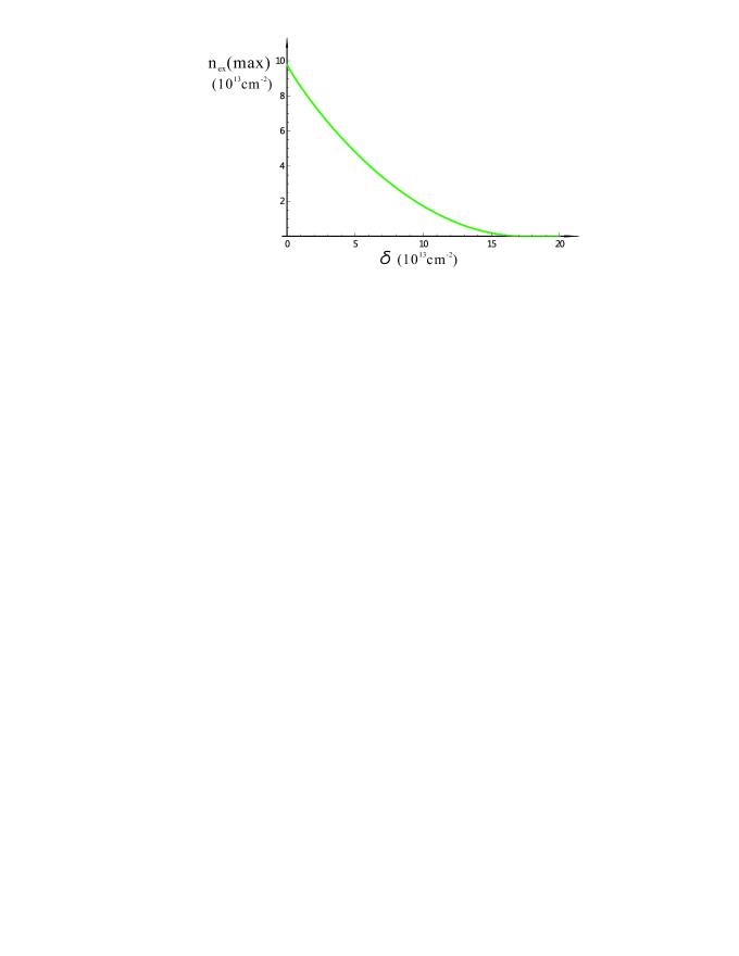
As seen from formula (34) for the neutral system, nexmaxβˆΌΟ‰2v2similar-tosuperscriptsubscript𝑛exmaxsuperscriptπœ”2superscript𝑣2n_{\text{ex}}^{\text{max}}\sim\frac{\omega^{2}}{v^{2}}, the available phase space rises with increasing pump frequency. On the other hand, phase space capacity decreases with increasing initial electron doping density, as expected.

However, for photoexcitation density nexsubscript𝑛exn_{\text{ex}} as an input parameter in our calculation, a critical question to ask is: does this maximal density nexmaxsuperscriptsubscript𝑛exmaxn_{\text{ex}}^{\text{max}} equal the saturation density nexsatsuperscriptsubscript𝑛exsatn_{\text{ex}}^{\text{sat}} in real pumping process, or in another word, can phase space be completely filled? We will answer this question later.

6.2.3 Doped System

Next we discuss the system away from the Dirac point with a finite electron doping, i.e., Ξ΄β‰₯0𝛿0\delta\geq 0 or x=Ξ΄nΒ―β‰₯0π‘₯𝛿¯𝑛0x=\frac{\delta}{\bar{n}}\geq 0, which is often the case, e.g., in epitaxial graphene on SiC substrate. In this case, from Eqs. (28)-(30) we obtain the expression of tesubscript𝑑𝑒t_{e} as a function of z+subscript𝑧z_{+}

te=(fex2+(te0)2​[βˆ’Li2​(βˆ’z0)]βˆ’Li2​(βˆ’z+))1/2,subscript𝑑𝑒superscriptsubscript𝑓ex2superscriptsuperscriptsubscript𝑑𝑒02delimited-[]subscriptLi2superscript𝑧0subscriptLi2subscript𝑧12t_{e}=\left(\frac{\frac{f_{\text{ex}}}{2}+\left(t_{e}^{0}\right)^{2}\left[-\mathrm{Li}_{2}(-z^{0})\right]}{-\mathrm{Li}_{2}(-z_{+})}\right)^{1/2}, (39)

then the coupled equations are reduced to

βˆ’Li2​(βˆ’1zβˆ’)=C1​[βˆ’Li2​(βˆ’z+)],subscriptLi21subscript𝑧subscript𝐢1delimited-[]subscriptLi2subscript𝑧-\mathrm{Li}_{2}\left(-\frac{1}{z_{-}}\right)=C_{1}\left[-\mathrm{Li}_{2}(-z_{+})\right], (40)
[βˆ’Li3​(βˆ’z+)βˆ’Li3​(βˆ’1zβˆ’)]2/3=C2​[βˆ’Li2​(βˆ’z+)],superscriptdelimited-[]subscriptLi3subscript𝑧subscriptLi31subscript𝑧23subscript𝐢2delimited-[]subscriptLi2subscript𝑧\left[-\mathrm{Li}_{3}\left(-z_{+}\right)-\mathrm{Li}_{3}\left(-\frac{1}{z_{-}}\right)\right]^{2/3}=C_{2}\left[-\mathrm{Li}_{2}(-z_{+})\right], (41)

with

C1​(fex)=1βˆ’xfex+2​(te0)2​[βˆ’Li2​(βˆ’z0)],subscript𝐢1subscript𝑓ex1π‘₯subscript𝑓ex2superscriptsuperscriptsubscript𝑑𝑒02delimited-[]subscriptLi2superscript𝑧0C_{1}(f_{\text{ex}})=1-\frac{x}{f_{\text{ex}}+2\left(t_{e}^{0}\right)^{2}\left[-\mathrm{Li}_{2}(-z^{0})\right]}, (42)
C2​(fex)=(fex​Ω4+(te0)3​[βˆ’Li3​(βˆ’z0)βˆ’Li3​(βˆ’1z0)])2/3fex2+(te0)2​[βˆ’Li2​(βˆ’z0)].subscript𝐢2subscript𝑓exsuperscriptsubscript𝑓exΞ©4superscriptsuperscriptsubscript𝑑𝑒03delimited-[]subscriptLi3superscript𝑧0subscriptLi31superscript𝑧023subscript𝑓ex2superscriptsuperscriptsubscript𝑑𝑒02delimited-[]subscriptLi2superscript𝑧0C_{2}(f_{\text{ex}})=\frac{\left(\frac{f_{\text{ex}}\Omega}{4}+\left(t_{e}^{0}\right)^{3}\left[-\mathrm{Li}_{3}\left(-z^{0}\right)-\mathrm{Li}_{3}\left(-\frac{1}{z^{0}}\right)\right]\right)^{2/3}}{\frac{f_{\text{ex}}}{2}+\left(t_{e}^{0}\right)^{2}\left[-\mathrm{Li}_{2}(-z^{0})\right]}. (43)

Solving the two equations (40) and (41) we obtain z+subscript𝑧z_{+} and zβˆ’subscript𝑧z_{-}, which in turn gives t𝑑t via Eq. (39). Finally, the physical quantities are derived through kB​Te=te​D,ΞΌ+=te​D​ln⁑z+,ΞΌβˆ’=te​D​ln⁑zβˆ’.formulae-sequencesubscriptπ‘˜Bsubscript𝑇𝑒subscript𝑑𝑒𝐷formulae-sequencesubscriptπœ‡subscript𝑑𝑒𝐷subscript𝑧subscriptπœ‡subscript𝑑𝑒𝐷subscript𝑧k_{\text{B}}T_{e}=t_{e}D,\ \mu_{+}=t_{e}D\ln z_{+},\ \mu_{-}=t_{e}D\ln z_{-}.

To show the numerical results, we choose the experimental system of graphene on SiC substrate with an initial electron doping Ξ΄=1.17Γ—1013​cmβˆ’2𝛿1.17superscript1013superscriptcm2\delta=1.17\times 10^{13}\text{cm}^{-2}, corresponding to an initial chemical potential ΞΌ0=0.4superscriptπœ‡00.4\mu^{0}=0.4eV, being excited by the pump energy ℏ​ω=1.55​eVPlanck-constant-over-2-piπœ”1.55eV\hbar\omega=1.55\text{eV}. The phase space capacity is calculated from Eq. (38) to be nexmax=8.34Γ—1013​cmβˆ’2superscriptsubscript𝑛exmax8.34superscript1013superscriptcm2n_{\text{ex}}^{\text{max}}=8.34\times 10^{13}\text{cm}^{-2} at this doping level. The electron temperature Tesubscript𝑇𝑒T_{e} (in units of Kelvin) changing with nexsubscript𝑛exn_{\text{ex}} (in units of 1013​cmβˆ’2superscript1013superscriptcm210^{13}\text{cm}^{-2}) is plotted in Fig. 10. Compared to the undoped system, the evolution of electron temperature with photoexcitation density is smoother and the electron temperature is lower due to the finite initial carrier density.

Refer to caption
Figure 10: Plot of the electron temperature Tesubscript𝑇𝑒T_{e} varying with photoexcitation density nexsubscript𝑛exn_{\text{ex}} in epitaxial graphene on SiC substrate with initial chemical potential ΞΌ0=0.4superscriptπœ‡00.4\mu^{0}=0.4eV. The non-monotonous behavior remains although the change of temperature with density is smoother compared to the neutral system.

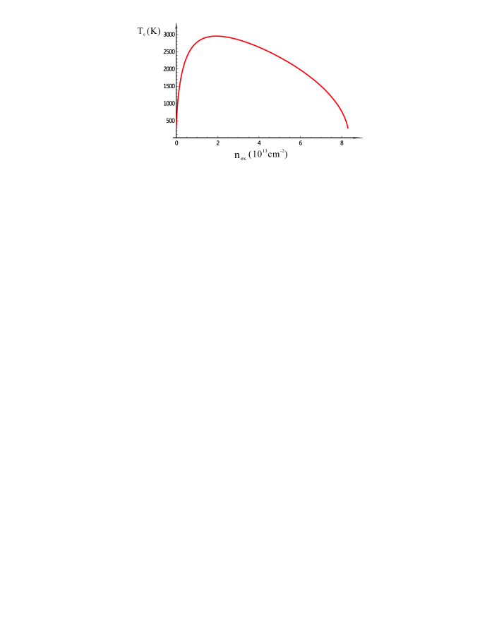
Figure 11 shows the upper- and lower-band chemical potential ΞΌ+subscriptπœ‡\mu_{+} and ΞΌβˆ’subscriptπœ‡\mu_{-} (in units of eV) varying with nexsubscript𝑛exn_{\text{ex}} (in units of 1013​cmβˆ’2superscript1013superscriptcm210^{13}\text{cm}^{-2}).

Refer to caption
Figure 11: Plot of the upper- and lower-band chemical potentials ΞΌ+subscriptπœ‡\mu_{+} and ΞΌβˆ’subscriptπœ‡\mu_{-}, in units of eV, varying with photoexcitation density nexsubscript𝑛exn_{\text{ex}} in epitaxial graphene on SiC substrate with initial chemical potential ΞΌ0=0.4superscriptπœ‡00.4\mu^{0}=0.4eV. The upper-band chemical potential remains positive although it drops a little bit at low densities, while the lower-band chemical potential drops rapidly at rather low densities followed by increasing separation from the upper-band chemical potential. Clearly, the upper- and lower-band chemical potentials are not symmetric as in the neutral system.

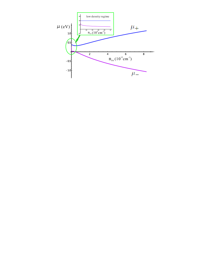
Clearly, due to the large initial electron-doping, the low-density classical gas phase for the upper-band electrons is absent now, although there is a tiny presence for the lower band. And in the doped case, the upper- and lower-band chemical potentials are not symmetric, ΞΌ+β‰ βˆ’ΞΌβˆ’subscriptπœ‡subscriptπœ‡\mu_{+}\neq-\mu_{-}, as they are in the neutral system. The separation between the two chemical potentials increases with photoexcitation density.

6.2.4 Broadband Distribution and Blueshifted Photoluminescence

A direct consequence to the high electron temperature Te∼3000βˆ’4000​Ksimilar-tosubscript𝑇𝑒30004000KT_{e}\sim 3000-4000\text{K} and the slow population relaxation is a broadband distribution of electron and hole excitations. This can be illustrated in the occupation number Ne,h​(Ξ΅)=D​(Ξ΅)​fe,h​(Ξ΅)subscriptπ‘π‘’β„Žπœ€π·πœ€subscriptπ‘“π‘’β„Žπœ€N_{e,h}(\varepsilon)=D(\varepsilon)f_{e,h}(\varepsilon), where D​(Ξ΅)=2​Ρπ​(ℏ​v)2π·πœ€2πœ€πœ‹superscriptPlanck-constant-over-2-pi𝑣2D(\varepsilon)=\frac{2\varepsilon}{\pi(\hbar v)^{2}} is the density of state at energy Ξ΅πœ€\varepsilon and fe,h​(Ξ΅)subscriptπ‘“π‘’β„Žπœ€f_{e,h}(\varepsilon) are the electron and hole distribution functions with fe=f+,fh=1βˆ’fβˆ’formulae-sequencesubscript𝑓𝑒subscript𝑓subscriptπ‘“β„Ž1subscript𝑓f_{e}=f_{+},\ f_{h}=1-f_{-}. Figure 12 shows the electron and hole distribution at different photoexcitation density in the neutral system and in the electron-doped system (ΞΌ0=0.4​eVsuperscriptπœ‡00.4eV\mu^{0}=0.4\text{eV}).

Refer to caption
Figure 12: Electron (blue line) and hole (green line) occupation number, in units of 2π​(ℏ​v)22πœ‹superscriptPlanck-constant-over-2-pi𝑣2\frac{2}{\pi(\hbar v)^{2}}, distributed with respect to energy at different photoexcitation density states. We can see the broadband distribution of photoexcited carriers with a high-temperature tail up to almost 2 eV.

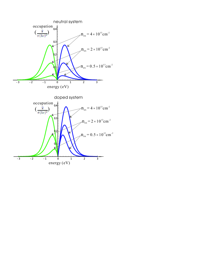
The high temperature tail in the distribution extends the excited carriers well above the excitation energy 1.55​eV1.55eV1.55\text{eV} up to 2-3eV. This coverage of higher energy states enables emission of photons with higher frequencies than that of the excitation photons, which exhibits blue-shift phenomena in the photoluminescence spectrum. This unusual blueshifted components have been observed in recent experiments[7, 8, 9] and is naturally explained in our model.

6.3 Optical Conductivity

Now we are back to the question raised before. In order to identify the saturation density, we need to study the optical responses of this electronic state at different photoexcitation densities. In this section, we calculate the optical conductivity for the nonequilibrium intermediate state using Keldysh technique. By analyzing its behavior at high densities, interesting optical properties are revealed.

6.3.1 General Formalism

The low-energy noninteracting Hamiltonian of graphene can be written in the band representation as

H0=vβ€‹βˆ‘a=1gβˆ«π€βˆ‘Ξ»=±λ​k​γa,λ†​(𝐀)​γa,λ​(𝐀)subscript𝐻0𝑣superscriptsubscriptπ‘Ž1𝑔subscript𝐀subscriptπœ†plus-or-minusπœ†π‘˜superscriptsubscriptπ›Ύπ‘Žπœ†β€ π€subscriptπ›Ύπ‘Žπœ†π€H_{0}=v\sum_{a=1}^{g}\int_{\mathbf{k}}\sum_{\lambda=\pm}\lambda k\gamma_{a,\lambda}^{\dagger}(\mathbf{k})\gamma_{a,\lambda}(\mathbf{k}) (44)

with Ξ»=+πœ†\lambda=+ or βˆ’- corresponding to the upper or lower band and Ξ³a,λ†​(𝐀),Ξ³a,λ​(𝐀)superscriptsubscriptπ›Ύπ‘Žπœ†β€ π€subscriptπ›Ύπ‘Žπœ†π€\gamma_{a,\lambda}^{\dagger}(\mathbf{k}),\ \gamma_{a,\lambda}(\mathbf{k}) are the operators that create or annihilate a quasiparticle of flavor aπ‘Ža (spin and valley) at the 2-dimensional wavevector 𝐀=(kx,ky)𝐀subscriptπ‘˜π‘₯subscriptπ‘˜π‘¦\mathbf{k}=(k_{x},k_{y}) in band Ξ»πœ†\lambda. In the band representation the current vertex becomes

𝐣^𝐀=e​v​(𝐀k​σzβˆ’π€Γ—πžzk​σy),subscript^π£π€π‘’π‘£π€π‘˜subscriptπœŽπ‘§π€subscriptπžπ‘§π‘˜subscriptπœŽπ‘¦\hat{\mathbf{j}}_{\mathbf{k}}=ev\left(\frac{\mathbf{k}}{k}\sigma_{z}-\frac{\mathbf{k}\times\mathbf{e}_{z}}{k}\sigma_{y}\right), (45)

where Οƒy,zsubscriptπœŽπ‘¦π‘§\sigma_{y,z} are Pauli matrices due to the chiral structure of the Dirac fermions in graphene. Note that we set ℏ≑1Planck-constant-over-2-pi1\hbar\equiv 1 during the derivation, but will recover it in the final results.

In Keldysh formalism, the bubble diagram contributing to the optical conductivity gives the real part as

Re​σα​β​(Ο‰)=gβ€‹Ο€Ο‰β€‹βˆ«d​ω′​d2​k(2​π)2​Tr​[j^α​𝐀​A^𝐀​(Ο‰β€²+Ο‰)​j^β​𝐀​N^𝐀​(Ο‰β€²)βˆ’j^α​𝐀​A^𝐀​(Ο‰β€²)​j^β​𝐀​N^𝐀​(Ο‰β€²+Ο‰)]ResubscriptπœŽπ›Όπ›½πœ”π‘”πœ‹πœ”π‘‘superscriptπœ”β€²superscript𝑑2π‘˜superscript2πœ‹2Trdelimited-[]subscript^𝑗𝛼𝐀subscript^𝐴𝐀superscriptπœ”β€²πœ”subscript^𝑗𝛽𝐀subscript^𝑁𝐀superscriptπœ”β€²subscript^𝑗𝛼𝐀subscript^𝐴𝐀superscriptπœ”β€²subscript^𝑗𝛽𝐀subscript^𝑁𝐀superscriptπœ”β€²πœ”\mathrm{Re}\sigma_{\alpha\beta}(\omega)=\frac{g\pi}{\omega}\int\frac{d\omega^{\prime}d^{2}k}{(2\pi)^{2}}\mathrm{Tr}\left[\hat{j}_{\alpha\mathbf{k}}\hat{A}_{\mathbf{k}}(\omega^{\prime}+\omega)\hat{j}_{\beta\mathbf{k}}\hat{N}_{\mathbf{k}}(\omega^{\prime})-\hat{j}_{\alpha\mathbf{k}}\hat{A}_{\mathbf{k}}(\omega^{\prime})\hat{j}_{\beta\mathbf{k}}\hat{N}_{\mathbf{k}}(\omega^{\prime}+\omega)\right] (46)

for the direction α​(Ξ²)=x,y𝛼𝛽π‘₯𝑦\alpha(\beta)=x,y in the 2D graphene layer with the definitions

A^𝐀​(Ο‰)subscript^π΄π€πœ”\displaystyle\hat{A}_{\mathbf{k}}(\omega) =\displaystyle= i2​π​(G^𝐀r​e​t​(Ο‰)βˆ’G^𝐀a​d​v​(Ο‰)),𝑖2πœ‹superscriptsubscript^πΊπ€π‘Ÿπ‘’π‘‘πœ”superscriptsubscript^πΊπ€π‘Žπ‘‘π‘£πœ”\displaystyle\frac{i}{2\pi}\left(\hat{G}_{\mathbf{k}}^{ret}(\omega)-\hat{G}_{\mathbf{k}}^{adv}(\omega)\right), (47)
N^𝐀​(Ο‰)subscript^π‘π€πœ”\displaystyle\hat{N}_{\mathbf{k}}(\omega) =\displaystyle= βˆ’i2​π​G^𝐀<​(Ο‰).𝑖2πœ‹superscriptsubscript^πΊπ€πœ”\displaystyle-\frac{i}{2\pi}\hat{G}_{\mathbf{k}}^{<}(\omega). (48)

Here the retarded and advanced Green’s functions are matrices in band representation

G^𝐀r​e​t/a​d​v​(Ο‰)=(1ω±i​0++ΞΌΒ―βˆ’v​k001ω±i​0++ΞΌΒ―+v​k)superscriptsubscript^πΊπ€π‘Ÿπ‘’π‘‘π‘Žπ‘‘π‘£πœ”1plus-or-minusπœ”π‘–superscript0Β―πœ‡π‘£π‘˜001plus-or-minusπœ”π‘–superscript0Β―πœ‡π‘£π‘˜\hat{G}_{\mathbf{k}}^{ret/adv}(\omega)=\left(\begin{array}[]{cc}\frac{1}{\omega\pm i0^{+}+\bar{\mu}-vk}&0\\ 0&\frac{1}{\omega\pm i0^{+}+\bar{\mu}+vk}\end{array}\right) (49)

where ++ (βˆ’-) sign associates with the retarded (advanced) Green’s function, and the lesser Green’s function is written as

G^𝐀<​(Ο‰)=(g𝐀,+<​(Ο‰)00g𝐀,βˆ’<​(Ο‰)),superscriptsubscript^πΊπ€πœ”superscriptsubscriptπ‘”π€πœ”00superscriptsubscriptπ‘”π€πœ”\hat{G}_{\mathbf{k}}^{<}(\omega)=\left(\begin{array}[]{cc}g_{\mathbf{k},+}^{<}(\omega)&0\\ 0&g_{\mathbf{k},-}^{<}(\omega)\end{array}\right), (50)
g𝐀,Β±<​(Ο‰)=2​π​i​f​(Ρ±​(k)βˆ’ΞΌΒ±)​δ​(Ο‰βˆ’Ξ΅Β±β€‹(k)+ΞΌΒ―),superscriptsubscript𝑔𝐀plus-or-minusπœ”2πœ‹π‘–π‘“subscriptπœ€plus-or-minusπ‘˜subscriptπœ‡plus-or-minusπ›Ώπœ”subscriptπœ€plus-or-minusπ‘˜Β―πœ‡g_{\mathbf{k},\pm}^{<}(\omega)=2\pi if(\varepsilon_{\pm}(k)-\mu_{\pm})\delta(\omega-\varepsilon_{\pm}(k)+\bar{\mu}), (51)

with ΞΌΒ―=12​(ΞΌ++ΞΌβˆ’)Β―πœ‡12subscriptπœ‡subscriptπœ‡\bar{\mu}=\frac{1}{2}\left(\mu_{+}+\mu_{-}\right) and the Fermi function f​(x)≑1ex/(kB​Te)+1.𝑓π‘₯1superscript𝑒π‘₯subscriptπ‘˜Bsubscript𝑇𝑒1f(x)\equiv\frac{1}{e^{x/(k_{\text{B}}T_{e})}+1}. Note that distinct chemical potentials are employed in the distribution functions to characterize the nonequilibrium state but an average chemical potential is used in the spectral functions to avoid an artificial modification of the spectrum.

Previous analysis (see Section 3) shows that the optical properties of graphene on an insulating substrate, such as reflection, transmission, and absorption, are fully determined by the real part of the optical conductivity Re​σ​(Ο‰)ReπœŽπœ”\mathrm{Re}\sigma(\omega) to leading order in the fine-structure constant of quantum electrodynamics Ξ±QED=e2ℏ​cβ‰ˆ1137β‰ͺ1subscript𝛼QEDsuperscript𝑒2Planck-constant-over-2-pi𝑐1137much-less-than1\alpha_{\text{QED}}=\frac{e^{2}}{\hbar c}\approx\frac{1}{137}\ll 1. The imaginary part only enters at higher orders. Therefore, we make direct connections of the real part conductivity to the optical responses observable in experiments.

From Eq.(46) we calculate the longitudinal conductivity which contains intraband and interband transitions. To show the transition processes specifically, introduce a𝐀,λ​(Ο‰)≑δ​(Ο‰βˆ’Ξ»β€‹v​k+ΞΌΒ―),and​fλ​(Ο‰)≑f​(Ο‰βˆ’Ξ»β€‹Ξ΄β€‹ΞΌ).formulae-sequencesubscriptπ‘Žπ€πœ†πœ”π›Ώπœ”πœ†π‘£π‘˜Β―πœ‡andsubscriptπ‘“πœ†πœ”π‘“πœ”πœ†π›Ώπœ‡a_{\mathbf{k},\lambda}(\omega)\equiv\delta(\omega-\lambda vk+\bar{\mu}),\ \text{and}\ f_{\lambda}(\omega)\equiv f(\omega-\lambda\delta\mu). It follows the intraband and interband conductivities

Re​σx​xintra​(Ο‰)Resuperscriptsubscript𝜎π‘₯π‘₯intraπœ”\displaystyle\mathrm{Re}\sigma_{xx}^{\text{intra}}(\omega)
=\displaystyle= g​π​(e​v)2β€‹βˆ«d​ω′​d2​k(2​π)2​cos2β‘ΞΈβ€‹βˆ‘Ξ»=Β±a𝐀,λ​(Ο‰β€²)​a𝐀,λ​(Ο‰β€²+Ο‰)​fλ​(Ο‰β€²)βˆ’fλ​(Ο‰β€²+Ο‰)Ο‰,π‘”πœ‹superscript𝑒𝑣2𝑑superscriptπœ”β€²superscript𝑑2π‘˜superscript2πœ‹2superscript2πœƒsubscriptπœ†plus-or-minussubscriptπ‘Žπ€πœ†superscriptπœ”β€²subscriptπ‘Žπ€πœ†superscriptπœ”β€²πœ”subscriptπ‘“πœ†superscriptπœ”β€²subscriptπ‘“πœ†superscriptπœ”β€²πœ”πœ”\displaystyle g\pi\left(ev\right)^{2}\int\frac{d\omega^{\prime}d^{2}k}{(2\pi)^{2}}\cos^{2}\theta\sum_{\lambda=\pm}a_{\mathbf{k},\lambda}(\omega^{\prime})a_{\mathbf{k},\lambda}(\omega^{\prime}+\omega)\frac{f_{\lambda}(\omega^{\prime})-f_{\lambda}(\omega^{\prime}+\omega)}{\omega},
Re​σx​xinter​(Ο‰)Resuperscriptsubscript𝜎π‘₯π‘₯interπœ”\displaystyle\mathrm{Re}\sigma_{xx}^{\text{inter}}(\omega)
=\displaystyle= g​π​(e​v)2β€‹βˆ«d​ω′​d2​k(2​π)2​sin2β‘ΞΈβ€‹βˆ‘Ξ»=Β±a𝐀,λ​(Ο‰β€²)​a𝐀,λ¯​(Ο‰β€²+Ο‰)​fλ​(Ο‰β€²)βˆ’fλ¯​(Ο‰β€²+Ο‰)Ο‰,π‘”πœ‹superscript𝑒𝑣2𝑑superscriptπœ”β€²superscript𝑑2π‘˜superscript2πœ‹2superscript2πœƒsubscriptπœ†plus-or-minussubscriptπ‘Žπ€πœ†superscriptπœ”β€²subscriptπ‘Žπ€Β―πœ†superscriptπœ”β€²πœ”subscriptπ‘“πœ†superscriptπœ”β€²subscriptπ‘“Β―πœ†superscriptπœ”β€²πœ”πœ”\displaystyle g\pi\left(ev\right)^{2}\int\frac{d\omega^{\prime}d^{2}k}{(2\pi)^{2}}\sin^{2}\theta\sum_{\lambda=\pm}a_{\mathbf{k},\lambda}(\omega^{\prime})a_{\mathbf{k},\bar{\lambda}}(\omega^{\prime}+\omega)\frac{f_{\lambda}(\omega^{\prime})-f_{\bar{\lambda}}(\omega^{\prime}+\omega)}{\omega}, (53)

where cos⁑θ=kxk,sin⁑θ=kykformulae-sequenceπœƒsubscriptπ‘˜π‘₯π‘˜πœƒsubscriptπ‘˜π‘¦π‘˜\cos\theta=\frac{k_{x}}{k},\ \sin\theta=\frac{k_{y}}{k}.

6.3.2 Intraband Transition

First let us evaluate intraband conductivity. It is straightforwardly obtained from Eq. (6.3.1)

Re​σx​xintra​(Ο‰)Resuperscriptsubscript𝜎π‘₯π‘₯intraπœ”\displaystyle\mathrm{Re}\sigma_{xx}^{\text{intra}}(\omega) =\displaystyle= g​(e​v)2(2)2Ξ΄(Ο‰)∫0∞kdk[βˆ’βˆ‚f​(Ο‰)βˆ‚Ο‰|Ο‰=v​kβˆ’ΞΌ+βˆ’βˆ‚f​(Ο‰)βˆ‚Ο‰|Ο‰=βˆ’v​kβˆ’ΞΌβˆ’]\displaystyle\frac{g\left(ev\right)^{2}}{(2)^{2}}\delta(\omega)\int_{0}^{\infty}kdk\left[-\frac{\partial f(\omega)}{\partial\omega}\Biggl{|}_{\omega=vk-\mu_{+}}-\frac{\partial f(\omega)}{\partial\omega}\Biggl{|}_{\omega=-vk-\mu_{-}}\right] (54)
=\displaystyle= e2ℏ​ln⁑[(1+z+)​(1+zβˆ’βˆ’1)]​kB​Te​δ​(Ο‰)superscript𝑒2Planck-constant-over-2-pi1subscript𝑧1superscriptsubscript𝑧1subscriptπ‘˜π΅subscriptπ‘‡π‘’π›Ώπœ”\displaystyle\frac{e^{2}}{\hbar}\ln\left[(1+z_{+})(1+z_{-}^{-1})\right]k_{B}T_{e}\delta(\omega)

where we have recovered the factor ℏPlanck-constant-over-2-pi\hbar on the last line. The delta-function will be replaced by a Lorentzian δ​(Ο‰)β†’Ο„βˆ’1Ο‰2+(Ο„βˆ’1)2β†’π›Ώπœ”superscript𝜏1superscriptπœ”2superscriptsuperscript𝜏12\delta(\omega)\rightarrow\frac{\tau^{-1}}{\omega^{2}+(\tau^{-1})^{2}} for further discussions, which is not our concern here. In equilibrium state z+=zβˆ’=z0=eβ​μ0subscript𝑧subscript𝑧superscript𝑧0superscript𝑒𝛽superscriptπœ‡0z_{+}=z_{-}=z^{0}=e^{\beta\mu^{0}}, the intraband conductivity becomes Re​σx​xintra​(Ο‰)=e2ℏ​[kB​Te0​ln⁑(2+eβ​μ0+eβˆ’Ξ²β€‹ΞΌ0)]​δ​(Ο‰)Resuperscriptsubscript𝜎π‘₯π‘₯intraπœ”superscript𝑒2Planck-constant-over-2-pidelimited-[]subscriptπ‘˜Bsuperscriptsubscript𝑇𝑒02superscript𝑒𝛽superscriptπœ‡0superscript𝑒𝛽superscriptπœ‡0π›Ώπœ”\mathrm{Re}\sigma_{xx}^{\text{intra}}(\omega)=\frac{e^{2}}{\hbar}\left[k_{\text{B}}T_{e}^{0}\ln(2+e^{\beta\mu^{0}}+e^{-\beta\mu^{0}})\right]\delta(\omega) which recovers the well-known expression in the neutral system at equilibrium Re​σx​xintra​(Ο‰)=2​ln⁑2​e2ℏ​kB​Te0​δ​(Ο‰),Resuperscriptsubscript𝜎π‘₯π‘₯intraπœ”22superscript𝑒2Planck-constant-over-2-pisubscriptπ‘˜Bsuperscriptsubscript𝑇𝑒0π›Ώπœ”\mathrm{Re}\sigma_{xx}^{\text{intra}}(\omega)=2\ln 2\frac{e^{2}}{\hbar}k_{\text{B}}T_{e}^{0}\delta(\omega), as expected.

The most interesting observation from the intraband transition for the transient electronic state is the modified Drude spectral weight

D=e2ℏ​ln⁑[(1+z+)​(1+zβˆ’βˆ’1)]​kB​Te,𝐷superscript𝑒2Planck-constant-over-2-pi1subscript𝑧1superscriptsubscript𝑧1subscriptπ‘˜π΅subscript𝑇𝑒D=\frac{e^{2}}{\hbar}\ln\left[(1+z_{+})(1+z_{-}^{-1})\right]k_{B}T_{e}, (55)

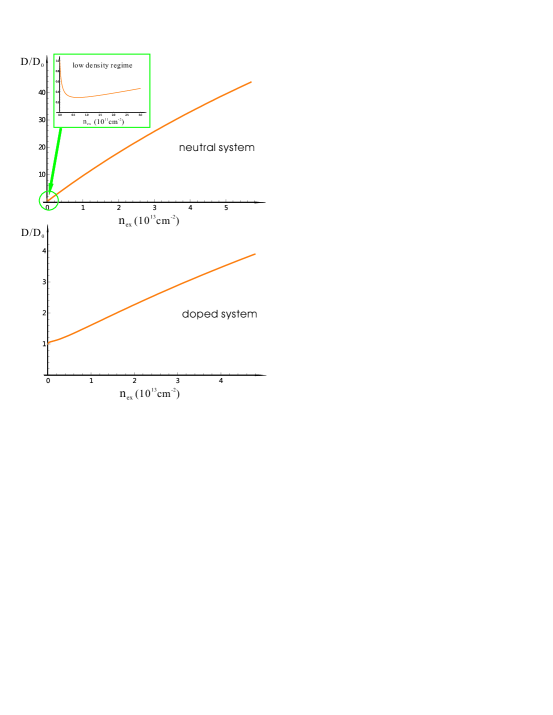
which can be significantly enhanced by the high electron temperature. But it could also be reduced when the reduction of chemical potential dominates at low densities in the neutral system. Here we show the Drude weight change, normalized by the equilibrium value D0=e2ℏ​ln⁑[(1+z0)​(1+1/z0)]​kB​Te0subscript𝐷0superscript𝑒2Planck-constant-over-2-pi1superscript𝑧011superscript𝑧0subscriptπ‘˜π΅superscriptsubscript𝑇𝑒0D_{0}=\frac{e^{2}}{\hbar}\ln\left[(1+z^{0})(1+1/z^{0})\right]k_{B}T_{e}^{0}, at different nexsubscript𝑛exn_{\text{ex}} in the neutral and electron-doped systems in Fig. 13.

The results for the neutral system exhibits a drop in Drude spectral weight at low densities due to the large drop in chemical potential as shown in Fig. 8 but quickly followed by large enhancement at higher densities. In the electron-doped system, Drude weight is always increasing but with much less enhancement than in the neutral system.

Refer to caption
Figure 13: Drude spectral weigh D𝐷D, normalized by the equilibrium value D0subscript𝐷0D_{0}, changes with photoexcitation density in neutral and doped (with initial chemical potential ΞΌ0=0.4​eVsuperscriptπœ‡00.4eV\mu^{0}=0.4\text{eV}) system. In neutral system it drops at low densities due to the large drop in chemical potential as shown in Fig. 8, but followed by a large enhancement at higher densities. In the doped system, it is always enhanced but with a much smaller enhancement factor than that of the neutral system.

6.3.3 Interband Transition

In order to understand the optical response at high frequencies, as optical conductivity is dominated by interband transition for frequencies on the order of 1eV, we evaluate the interband conductivity from Eq.(53),

Re​σx​xinter​(Ο‰)Resuperscriptsubscript𝜎π‘₯π‘₯interπœ”\displaystyle\mathrm{Re}\sigma_{xx}^{\text{inter}}(\omega) =\displaystyle= g​(e)2(2)4​[f​(βˆ’Ο‰2βˆ’ΞΌβˆ’)βˆ’f​(Ο‰2βˆ’ΞΌ+)]𝑔superscript𝑒2superscript24delimited-[]π‘“πœ”2subscriptπœ‡π‘“πœ”2subscriptπœ‡\displaystyle\frac{g\left(e\right)^{2}}{(2)^{4}}\left[f(-\frac{\omega}{2}-\mu_{-})-f(\frac{\omega}{2}-\mu_{+})\right] (56)
=\displaystyle= e24​ℏ​12​[tanh⁑(ℏ​ω+2β€‹ΞΌβˆ’4​kB​Te)+tanh⁑(β„β€‹Ο‰βˆ’2​μ+4​kB​Te)]superscript𝑒24Planck-constant-over-2-pi12delimited-[]Planck-constant-over-2-piπœ”2subscriptπœ‡4subscriptπ‘˜π΅subscript𝑇𝑒Planck-constant-over-2-piπœ”2subscriptπœ‡4subscriptπ‘˜π΅subscript𝑇𝑒\displaystyle\frac{e^{2}}{4\hbar}\frac{1}{2}\left[\tanh\left(\frac{\hbar\omega+2\mu_{-}}{4k_{B}T_{e}}\right)+\tanh\left(\frac{\hbar\omega-2\mu_{+}}{4k_{B}T_{e}}\right)\right]

where the probe photon frequency Ο‰>0πœ”0\omega>0 and we have reinserted the factor ℏPlanck-constant-over-2-pi\hbar on the last line. In equilibrium state, ΞΌ+=ΞΌβˆ’=ΞΌ0subscriptπœ‡subscriptπœ‡superscriptπœ‡0\mu_{+}=\mu_{-}=\mu^{0}, the interband transition becomes Re​σx​xinter​(Ο‰)=e24​ℏ​12​[tanh⁑(ℏ​ω+2​μ04​kB​Te0)+tanh⁑(β„β€‹Ο‰βˆ’2​μ04​kB​Te0)]Resuperscriptsubscript𝜎π‘₯π‘₯interπœ”superscript𝑒24Planck-constant-over-2-pi12delimited-[]Planck-constant-over-2-piπœ”2superscriptπœ‡04subscriptπ‘˜π΅superscriptsubscript𝑇𝑒0Planck-constant-over-2-piπœ”2superscriptπœ‡04subscriptπ‘˜π΅superscriptsubscript𝑇𝑒0\mathrm{Re}\sigma_{xx}^{\text{inter}}(\omega)=\frac{e^{2}}{4\hbar}\frac{1}{2}\left[\tanh\left(\frac{\hbar\omega+2\mu^{0}}{4k_{B}T_{e}^{0}}\right)+\tanh\left(\frac{\hbar\omega-2\mu^{0}}{4k_{B}T_{e}^{0}}\right)\right] which gives the expression for the neutral system in equilibrium Re​σx​xinter​(Ο‰)=e24​ℏ​tanh⁑(ℏ​ω4​kB​Te0)Resuperscriptsubscript𝜎π‘₯π‘₯interπœ”superscript𝑒24Planck-constant-over-2-piPlanck-constant-over-2-piπœ”4subscriptπ‘˜π΅superscriptsubscript𝑇𝑒0\mathrm{Re}\sigma_{xx}^{\text{inter}}(\omega)=\frac{e^{2}}{4\hbar}\tanh\left(\frac{\hbar\omega}{4k_{B}T_{e}^{0}}\right), as expected.

By studying the optical response to different photon energies at various photoexcitation densities, unusual optical properties of the transient electronic state are found, which will be discussed in the following.

Femtosecond Absorption Saturation and Perfect Transparency

Let us first consider the optical response to the pump frequency. An interesting observation from the interband transition formula (56) arises due to the two density-dependent chemical potentials. As shown in Fig.8 and 11, with increasing photoexcitation density, the separation of the two chemical potentials also gets larger. Then at a certain photoexcitation density such that

ΞΌ+βˆ’ΞΌβˆ’=ℏ​ω,subscriptπœ‡subscriptπœ‡Planck-constant-over-2-piπœ”\mu_{+}-\mu_{-}=\hbar\omega, (57)

the optical conductivity vanishes and the system becomes perfect transparent. For higher densities, ΞΌ+βˆ’ΞΌβˆ’>ℏ​ωsubscriptπœ‡subscriptπœ‡Planck-constant-over-2-piπœ”\mu_{+}-\mu_{-}>\hbar\omega such that optical conductivity turns into negative, which implies a stimulated emission to keep the photoexcitation density from rising. This indicates that the absorption reaches zero and the number of excited carriers saturates at this density nexsatsuperscriptsubscript𝑛exsatn_{\text{ex}}^{\text{sat}} , which is stabilized by stimulated emission.

To show the variation of optical conductivity with photoexcitation density, we again calculate for the neutral system and the electron-doped system with initial doping ΞΌ0=0.4superscriptπœ‡00.4\mu^{0}=0.4eV by applying pump photon energy at ℏ​ω=1.55​eVPlanck-constant-over-2-piπœ”1.55eV\hbar\omega=1.55\text{eV}. We show the results in Fig.14 where they are normalized by the equilibrium value Οƒ0=e24​ℏsubscript𝜎0superscript𝑒24Planck-constant-over-2-pi\sigma_{0}=\frac{e^{2}}{4\hbar}.

Refer to caption
Figure 14: Interband conductivity σ​(ℏ​ω=1.55​eV)𝜎Planck-constant-over-2-piπœ”1.55eV\sigma(\hbar\omega=1.55\text{eV}), normalized by the equilibrium value Οƒ0=e24​ℏsubscript𝜎0superscript𝑒24Planck-constant-over-2-pi\sigma_{0}=\frac{e^{2}}{4\hbar}, varies with photoexcitation density nexsubscript𝑛exn_{\text{ex}} in the neutral and doped systems. It reaches zero, which indicates complete bleaching of absorption, at 5.7Γ—1013​cmβˆ’25.7superscript1013superscriptcm25.7\times 10^{13}\text{cm}^{-2} in the neutral system and 4.8Γ—1013​cmβˆ’24.8superscript1013superscriptcm24.8\times 10^{13}\text{cm}^{-2} in the doped system, corresponding to the saturation densities.

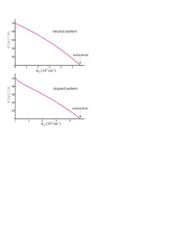
In both cases, the conductivity monotonously decreases due to the increasing electron temperature and separation of chemical potentials. The neutral system saturates at nexsat​(theory)=5.7Γ—1013​cmβˆ’2superscriptsubscript𝑛exsattheory5.7superscript1013superscriptcm2n_{\text{ex}}^{\text{sat}}(\text{theory})=5.7\times 10^{13}\text{cm}^{-2} while the electron-doped system saturates at roughly nexsat​(theory)=4.8Γ—1013​cmβˆ’2superscriptsubscript𝑛exsattheory4.8superscript1013superscriptcm2n_{\text{ex}}^{\text{sat}}(\text{theory})=4.8\times 10^{13}\text{cm}^{-2}. On the other hand, experimental measurement of the electron-doped system gives nexsat​(expt.)=5.0Γ—1013​cmβˆ’2superscriptsubscript𝑛exsatexpt.5.0superscript1013superscriptcm2n_{\text{ex}}^{\text{sat}}(\text{expt.})=5.0\times 10^{13}\text{cm}^{-2}, as shown in Fig. 6b, which is in excellent agreement with the theoretical value 4.8Γ—1013​cmβˆ’24.8superscript1013superscriptcm24.8\times 10^{13}\text{cm}^{-2}. This corroborates the correct description of the transient electronic state in our model. And it also answers the early posted question: the system saturates at a lower photoexcitation density before completely filling the available phase space, i.e., nexsat<nexmaxsuperscriptsubscript𝑛exsatsuperscriptsubscript𝑛exmaxn_{\text{ex}}^{\text{sat}}<n_{\text{ex}}^{\text{max}}.

Refer to caption
Figure 15: The calculated interband conductivity σ​(Ο‰)πœŽπœ”\sigma(\omega), normalized by the equilibrium value Οƒ0=e24​ℏsubscript𝜎0superscript𝑒24Planck-constant-over-2-pi\sigma_{0}=\frac{e^{2}}{4\hbar}, at higher (ℏ​ω=1.7​eVPlanck-constant-over-2-piπœ”1.7eV\hbar\omega=1.7\text{eV}, green line), the pump (ℏ​ω=1.55​eVPlanck-constant-over-2-piπœ”1.55eV\hbar\omega=1.55\text{eV}, magenta line), and lower (ℏ​ω=1.2​eVPlanck-constant-over-2-piπœ”1.2eV\hbar\omega=1.2\text{eV}, blue line) frequency. It shows that in the vicinity of saturation density the optical conductivity at lower frequencies (but still high enough to mainly detect interband transition) becomes negative. This indicates a stimulated emission that enables an optical gain for the low-frequency probes.

This theoretical calculation of an optical gain can serve as a test of our model, which have been used to simulate the optical differential reflectivity data performed in Fig. 5b (red line). The agreement is excellent.

Femtosecond Stimulated Emission and Optical Gain

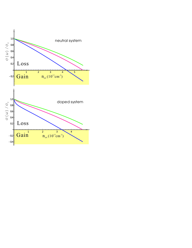
It is easy to see that higher-frequency pump will saturate at higher density since it can open up more phase space. Then when applying a probe with frequency higher than the pump frequency, we will expect it can not detect the zero absorption, as long as it is still within the low-energy Dirac spectrum, as shown in Fig.15 (green line). However, if one applies a lower-frequency probe, but not too low such that it is still mainly detecting the change in interband transition, one would expect an optical gain in the vicinity of the saturation density, as the optical conductivity becomes negative in this regime as shown in Fig.15 (blue line, yellow region). The appearance of negative conductivity signifies a stimulated emission that drives the system to a lower density as illustrated in Fig.2. We stress that the transient conductivity is negative in a regime below the pump frequency but above a certain frequency below which intraband transition becomes dominant.

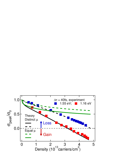
Comparison of Two Model Calculations with Pump-probe Spectroscopy Measurements

Here we further compare the calculated optical conductivity from the distinct-ΞΌπœ‡\mu model (ΞΌ+β‰ ΞΌβˆ’subscriptπœ‡subscriptπœ‡\mu_{+}\neq\mu_{-}) discussed above and the equal-ΞΌπœ‡\mu model (ΞΌ+=ΞΌβˆ’subscriptπœ‡subscriptπœ‡\mu_{+}=\mu_{-}) with the experimental value measured at probe photon energy ℏ​ω=1.55​eV​and​ 1.16​eVPlanck-constant-over-2-piπœ”1.55eVand1.16eV\hbar\omega=1.55\text{eV}\ \text{and}\ 1.16\text{eV} for a pump energy at ℏ​ω=1.55​eVPlanck-constant-over-2-piπœ”1.55eV\hbar\omega=1.55\text{eV}. As shown in Fig.16, we compare the experimentally-extracted, transient conductivity at 40 fs [18] with the calculated conductivity σ​(Ο‰)πœŽπœ”\sigma(\omega) as a function of the photoexcited carrier density nexsubscript𝑛exn_{\text{ex}} for two probe photon energies 1.55 eV and 1.16 eV. The Fermi energy of the sample is ∼0.4similar-toabsent0.4\sim 0.4 eV. The model calculation with the distinct chemical potentials reproduces the salient features of the experiment including nonlinear saturation and optical gain. Excellent agreement between experiment and theory also demonstrates a faithful representation of the transient state at 40 fs by the model described in the manuscript. The model calculation with the same chemical potential clearly fails to account for the experimental observations. For the degenerate scheme, our theory (black dashed line) yields Οƒβ†’0β†’πœŽ0\sigma\rightarrow 0 and thus perfect transparency at nex=4.8Γ—1013​cmβˆ’2subscript𝑛ex4.8superscript1013superscriptcm2n_{\text{ex}}=4.8\times 10^{13}\text{cm}^{-2}. Once the system is driven into this regime, a balance between stimulated emission and absorption will lead to a transparency. For non-degenerate scheme by probing at 1.16 eV, our theory (black solid line) predicts a critical density 3.2Γ—1013​cmβˆ’23.2superscript1013superscriptcm23.2\times 10^{13}\text{cm}^{-2} for the transition from loss to gain. All of these results agree quantitatively with the experimental values 5.0Γ—1013​cmβˆ’25.0superscript1013superscriptcm25.0\times 10^{13}\text{cm}^{-2} and 3.4Γ—1013​cmβˆ’23.4superscript1013superscriptcm23.4\times 10^{13}\text{cm}^{-2}, respectively.

Refer to caption
Figure 16: Comparison of the calculation from the distinct-ΞΌπœ‡\mu model (ΞΌ+β‰ ΞΌβˆ’subscriptπœ‡subscriptπœ‡\mu_{+}\neq\mu_{-}) and the equal-ΞΌπœ‡\mu model (ΞΌ+=ΞΌβˆ’subscriptπœ‡subscriptπœ‡\mu_{+}=\mu_{-}) with the experimentally measured transient optical conductivity at 40 fs after the 1.55eV pump at varying pump fluence. The probe photon energies are ℏ​ω=1.55​eVPlanck-constant-over-2-piπœ”1.55eV\hbar\omega=1.55\text{eV} (blue solid square) and 1.16​eV1.16eV1.16\text{eV} (red solid square). Clearly, the distinct-ΞΌπœ‡\mu model calculation of the conductivity at 1.55eV (black dashed line) and 1.16eV (black solid line) agrees quantitatively with the experimental data, in sharp contrast to the equal-ΞΌπœ‡\mu model results (green dashed line for 1.55eV and green solid line for 1.16eV). For the probe photon at lower frequency 1.16eV in the non-degenerate scheme, the transient conductivity becomes negative above a critical density exhibiting a transition from optical loss to gain, predicted by distinct-ΞΌπœ‡\mu model and substantiated by experiment.

7 Conclusions

We have studied the electronic state in photoexcited graphene formed via rapid carrier-carrier scattering after strong photoexcitation but before energy relaxation that takes place on a longer time scale. We have provided evidence for the existence of pronounced femtosecond population inversion and broadband gain in strongly photoexcited graphene monolayers. These results clearly reveal the transient electron and hole potentials are separated on the time scale of 100s of fs. By characterizing the state in terms of two separate Fermi-Dirac distributions with a common electron temperature but distinct chemical potentials for the upper and lower bands, we showed that this intermediate electronic state is associated with high electron temperature Tesubscript𝑇𝑒T_{e} up to 3000-4000K, which causes a broadband distribution extended to higher energy and is responsible for the observed blueshifted photoluminescence component. The analysis on the variation of electron temperature and chemical potentials with photoexcited carrier density in the neutral system clearly shows a crossover from hot dilute classical gas to dense quantum degenerate fermions. And unlike the phase space restriction in most semiconductors for a pump pulse on the order of 10fs, which is determined by the density of state at the optical excitation and the frequency width of the pulse, the fast depletion of phase space in graphene yields a broadband filling which significantly enlarge the accommodation of photoexcited carriers.

We thank Myron Hupalo and Michael Tringides for discussions. J.Z. acknowledges support by the Jeffress Memorial Trust, Grant No. J-1033. J.S. thanks the DFG Center for Functional Nanostructures. J.W. and T.L. acknowledge support by the the National Science Foundation (contract no. DMR-1055352). Work at Ames Laboratory was partially supported by the U.S. Department of Energy, Office of Basic Energy Science, Division of Materials Sciences and Engineering (Ames Laboratory is operated for the U.S. Department of Energy by Iowa State University under Contract No. DE-AC02-07CH11358).


References

  • [1] R.R. Nair, P. Blake, A.N. Grigorenko, K.S. Novoselov, T.J. Booth, T. Stauber, N.M.R. Peres, and A.K. Gaim 2008 Science 320, 1308.
  • [2] K.F. Mak, M.Y. Sfeir, Y. Wu, C.H. Lui, J.A. Misewich, and T.F. Heinz 2008 Phys. Rev. Lett. 101, 196405.
  • [3] A.H. Castro Neto, F. Guinea, N.M.R. Peres, K.S. Novoselov, and A.K. Geim 2009 Rev. Mod. Phys. 81, 109.
  • [4] F. Bonaccorso, Z. Sun, T. Hasan, and A.C. Ferrari 2010 Nature Photonics 4, 611.
  • [5] D. Sun, Z.-K. Wu, C. Divin, X. Li, C. Berger, W.A. de Heer, P.N. First, and T.B. Norris 2008 Phys. Rev. Lett. 101, 157402.
  • [6] H. Choi, F. Borondics, D.A. Siegel, S.Y. Zhou, M.C. Martin, A. Lanzara, and R.A. Kaindl 2009 Appl. Phys. Lett. 94, 172102.
  • [7] C.-H. Lui, K.F. Mak, J. Shan, and T.F. Heinz 2010 Phys. Rev. Lett. 105, 127404.
  • [8] W.-T. Liu, S.W. Wu, P.J. Schuck, M. Salmeron, Y.R. Shen, and F. Wang 2010 Phys. Rev. B 82, 081408(R).
  • [9] R.J. St?hr, R. Kolesov, J. Pflaum, and J. Wrachtrup 2010 Phys. Rev. B 82, 121408(R).
  • [10] J.M. Dawlaty, S. Shivaraman, M. Chandrashekhar, F. Rana, and M.G. Spencer 2008 Appl. Phys. Lett. 92, 042116.
  • [11] P.A. George, J. Strait, J. Dawlaty, S. Shivaraman, M. Chandrashekhar, F. Rana, and M.G. Spencer, 2008 Nano Lett. 8, 4248.
  • [12] M. Breusing, C. Ropers, and T. Elsaesser 2009 Phys. Rev. Lett. 102, 086809.
  • [13] R.W. Newson, J. Dean, B. Schmidt, and H.M. van Driel 2009 Optics Express 17, 2326.
  • [14] Steve Gilbertson, Georgi L. Dakovski, Tomasz Durakiewicz, Jian-Xin Zhu, Keshav M. Dani, Aditya D. Mohite, Andrew Dattelbaum and George Rodriguez 2012 J. Phys. Chem. Lett. 3, 64-68.
  • [15] K. M. Dani, J. Lee1, R. Sharma, A. D. Mohite1, C. M. Galande, P. M. Ajayan, A. M. Dattelbaum, H. Htoon, A. J. Taylor and R. P. Prasankumar 2012 Phys. Rev. B 86, 125403
  • [16] V. Ryzhii, M. Ryzhii and T. Otsuji 2007 J. Appl. Phys. 101, 083114
  • [17] S. Boubanga-Tombet, S. Chan, T. Watanabe, A. Satou, V. Ryzhii and T. Otsuji1, 2012 Phys. Rev. B 85, 035443
  • [18] T. Li, L. Luo, M. Hupalo, J. Zhang, M.C. Tringides, J. Schmalian and J. Wang, 2012 Phys. Rev. Lett. 108, 167401
  • [19] S Winnerl, et.al. 2013 J. Phys.: Condens. Matter 25, 054202
  • [20] Torben Winzer, Ermin Malic and Andreas Knorr 2012 arXiv:1209.4833
  • [21] B. Y. Sun, M. W. Wu 2012 arXiv:1302.3677
  • [22] L. Fritz, J. Schmalian, M. Muller, and S. Sachdev 2008 Phys. Rev. B 78, 085416.
  • [23] W.-K. Tse and S. Das Sarma 2009 Phys. Rev. B 79, 235406.
  • [24] R. Bistritzer and A. H. MacDonald 2009 Phys. Rev. Lett. 102, 206410.
  • [25] T. Winzer, A. Knorr, and E. Malic 2010 Nano Lett. 10, 4839.
  • [26] M.S. Foster and I.L. Aleiner 2009 Phys. Rev. B 79, 085415.
  • [27] J. Wang, et al. 2004 Physica E 20, 412.
  • [28] G.D. Sanders, et al. 2005 Phys. Rev. B 72, 245302.
  • [29] J. Wang, et al. 2009 Appl. Phys. Lett. 94, 021101.
  • [30] Jigang Wang, et al., 2010 Phys. Rev. Lett. 104, 177401.
  • [31] Jigang Wang, et al., 2004 Journal of Modern Optics, 51, 2771.
  • [32] Li, T. et.al., Nature in press, DOI 10.1038/nature11934 (2013).
  • [33] M. Hupalo, E. H. Conrad, M. C. Tringides, 2009 Phys. Rev. B 80, 041401(R).
  • [34] I. Forbeaux, J.-M. Themlin, and J.-M. Debever 2002 J. Appl. Phys. 92, 2479.
  • [35] C. Riedl, U. Starke, J. Bernhardt, M. Franke , and K. Heinz 2007 Phys. Rev. B 76, 245406.
  • [36] Myron Hupalo, Xiaojie Liu, Cai-Zhuang Wang, Wen-Cai Lu, Yon-Xin Yao, Kai-Ming Ho, Michael C. Tringides, et al., 2011 Advanced Materials, 23, 2082
  • [37] I. Gierz, C. Riedl, U. Starke, C. R. Ast, K. Kern 2008 Nano Lett, 8, 4603.
  • [38] S. Y. Zhou, G.-H. Gweon, A. V. Fedorov, P. N. First, W. A. de Heer, D.-H. Lee, F. Guinea, A. H. Castro Neto, and A. Lanzara, 2007 Nat. Mater. 6, 770.
  • [39] Isabella Gierz et al. 2010 Phys. Rev. B 81, 235408.
  • [40] Kin Fai Mak, Matthew Y. Sfeir, Yang Wu, Chun Hung Lui, James A. Misewich, and Tony F. Heinz 2008 Phys. Rev. Lett. 101, 196405.
  • [41] Born and E. Wolf, Principles of Optics (Cambridge University Press, Cambridge, UK, 1999).