Study of the itinerant electron magnetism of Fe-based superconductors by the proximity effect
Abstract
We used the proximity effect as a tool to achieve an ideal ("barrier-free") NS boundary for quantitative evaluation of transport phenomena that accompany converting dissipative current into supercurrent in NS systems with unconventional superconductors – single-crystal chalcogenide FeSe and granulated pnictide LaO(F)FeAs. Using features (limitations) of Andreev reflection in the NS systems with dispersion of the electron spin subbands, we revealed direct evidence for spin-polarized nature of transport and the absence of residual magnetization in iron-based superconductors in the normal state: In heterocontacts with single-crystal FeSe and granular LaO(F)FeAs, we detected a spin-dependent contribution to the efficiency of the Andreev reflection associated with the spin accumulation at the NS boundary, and a hysteresis of conductivity of FeSe in the ground state in low external magnetic fields. Based on our findings, we conclude that in iron-based superconductors, the itinerant electron magnetism is predominant, magnetism of iron atoms being localized.
1 Introduction
Along with the discovery of superconductivity in multi-component compounds with elements having significant local magnetic moment (Fe, Ni) [1], the detection of the same phenomenon in two-component compounds with the same elements proved to be an important discovery [2, 3]. Thus, a number of multi-component superconducting compounds of different composition, including iron-based, is closed by a compound directly adjacent to the family of single-element conventional superconductors. In this regard, there is no doubt that the appearance of superconductivity in multi-element compounds with delocalized electrons is closely related to the reduced symmetry of the crystal, in particular, such as the symmetry of "layered" type. This symmetry is characteristic of structures in a large family of compounds, containing a wide range of rare earths, pniktogens, chalcogens, and transition elements Mn, Fe, Co, Ni, Cu, and Ru. It leads to the anisotropy of the electronic and magnetic properties accompanied by an increased electron density of states in the layers with quasi-two-dimensional (anisotropic) Fermi surface and by an increased role of electron-electron interaction. Anisotropy of the properties seems to be that feature under which condition in the same material, the magnetic interactions coexist with the interactions that generate superconducting pairing of the excitations in the electron subsystem of layered superconductors of complex composition, including iron-based ones.
By now, the notion of crystal structures of layered superconductors and the nature of coupling in them is sufficiently developed and experimentally established, while their magnetic and electronic structures in the ground state are still a subject of debate and active research. In this regard, it is of considerable interest to compare electronic properties of layered iron superconductors which share the crystal structure of PbO type (P4/nmm) that predetermines related quasi-two-dimensional structures of the electronic bands with nesting [4 - 6]; relevant examples are the binary phase - FeSe and oxypnictide LaO(F)FeAs.
Theoretical collective efforts using local density of states approximation (see, eg, [4, 7, 8]) lead to the conclusion that the mechanism of superconductivity in iron-based pnictides and chalcogenides is likely to have nothing to do with the electron-phonon mechanism, even when the value of the critical temperature, , does not extend beyond the McMillan criterion [9], based on the values of the coupling constants and phonon dispersion characteristic of the electron-phonon pairing concept. This conclusion is sufficiently proved, despite the fact that the calculations "from the first principles" by the density functional method can give certain ambiguity in the definition of density of states and, as a consequence, of the band structure at the Fermi level [10 - 12]. In any case, the main argument in favor of this conclusion is as follows: The superconductivity in the presence of magnetic elements is observed in a wide range of compounds with layered crystalline structure of the same type and in a wide range of critical temperatures both satisfying and not satisfying (exceeding) the electron-phonon criterion.
One of the common methods of studying the electronic properties of superconductors is, as known, the investigation of the Andreev conductance, , of NS interfaces, either artificially created (heterosystems) or naturally produced in a homogeneous material, in the form of wide or narrow channels [13]. As the number of open Andreev levels () is directly proportional to the cross section of the interface, ( is the Fermi wavelength of an electron), it is clear that to study Andreev conductance is generally preferable to use wide channels. In this case, the only inconvenience for an experimenter, in the absence of artificial barriers on the interface (z = 0 where z is a parameter characterizing the energy barrier strength), is essentially low resistance of the channels. Intrinsic barrier height and a corresponding resistance which we will call an own resistance of the interface (known as the "Sharvin resistance" of restrictions [14]), are inversely proportional to the cross section of the interface: (here, are the charge, the Fermi momentum and velocity, the concentration and density of states per spin for free electrons, respectively).
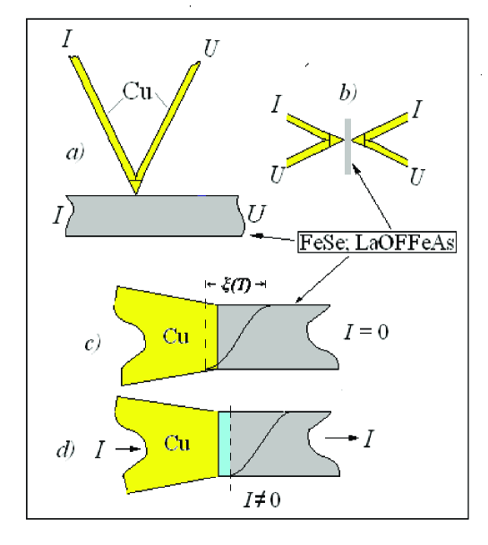
For substances with the conductivity of conventional metals, if is expressed in cm2. It follows that the restrictions (interfaces) with a diameter of the order of m cannot have an own resistance exceeding . Greater values often demonstrated by real point contacts indicate that, along with the resistive contribution from the interfaces , dissipative contributions exist from extraneous inclusions, such as parts of a probe (eg, the tip of the scanning probe) or defective or oxide barriers. In most cases, this is due to the fact that a "four-probe" method of measuring the current-voltage characteristics (IVC) when applying to point contacts, appears to be essentially two-contact one (see Fig. 1 a, b). That is why an area of incomparably greater length than ballistic one is forced to be measured; therefore, not only own contribution from the interface in the ballistic approximation is gauged [15]. In other words, the real contacts of point geometry, in general, cannot be considered ballistic in case of electrical measurements [16].
Physics of such contacts includes several mechanisms controlling the value of the system conductance in the NS state of the interface. After the system switches from the NN to NS state, total resistance of a real point contact, , contains at least the following additive contributions: (i) a dissipative contribution from the N - side of the interface of the total length of (by this we mean an overall contribution from a part of the tip, from an oxide layer, and from the layer which thickness measures alike the coherence length where the scattering cross section by impurities doubles under Andreev retroreflection [17]); (ii) an own contribution from the interface with the weight determined by the efficiency of the Andreev reflection which is a function of the energy parameters of the system (electron energy and the energy gap of a superconductor [15]); (iii) a dissipative contribution from the part of a superconductor related to the dispersion of the order parameter at the NS interface [18] due to the proximity effect. At the NN NS transition, the contribution (i) generally decreases the conductance of the contact and the contribution (ii) increases it. Previously, we have shown [16] that in a barrier-free non-ballistic contact, the contribution (i), in general, should prevail over the contribution (ii) within the energy range ; here, are the temperature, bias voltage, electron mean free path in the N – side, and the critical temperature of the superconductor, respectively.
Among these contributions, the contribution (iii) is the least known, especially that aspect of the proximity effect which is associated with the ability to generate a perfect NS boundary. Indeed, due to the dispersion, the order parameter at the NS boundary changes from 1 to 0 over the spatial range of the order of the Ginsburg-Landau characteristic length scale (Fig. 1 c). This means that the NS boundary can be moved by a macroscopic magnetic field of the transport current, no matter how small it is, deep into the superconductor, as shown in the Figure, provided that that field can suppress the superconductivity in the S-side of the contact. Thus, at finite values of the transport current, the NS boundary can be an ideal interface between the two parts of the same superconducting material which are in different states - normal and superconducting.
In this paper, we used this feature of the proximity effect for studying the nature of the magnetism of the ground state in new iron-based superconductors, chalcogenide FeSe and oxypnictide La[O1-xFx]FeAs. One might hope that the absence of extraneous inclusions at the NS boundary, often with uncontrolled characteristics that reduce the informativeness of Andreev reflection phenomenon, allows to judge with certainty about the presence or absence of the dispersion of the spin subbands in the normal ground state of a superconductor. Thus, we will be able to understand whether magnetism (and, indirectly, superconductivity) of iron-based superconductors is mainly itinerant and long-range phenomenon or localized and short-range one. Since the contributions (i) and (iii) are directly proportional to the thickness of the respective layers, their weight should be more noticeable as a total length of the NS sample approaches these thicknesses. Hence, we are led to maximum possible "shortening" of this length, ie, to a point-contact geometry of the samples and to the schemes for measuring CVC shown in Fig. 1 and corresponding, as explained above, with a two-contact measurement design. Here, we present the results of the research of Andreev conductance of non-ballistic point-contact NS heterostructures with relatively wide interfaces (of the area ). We study the systems Cu/FeSe and Cu/La[O1-xFx]FeAs.
2 Experiment
Starting materials of the superconductors used for preparing hybrid samples with point-contact geometry have a different structure in line with the technology of their preparation. Pnictide La[O0.85F0.1]FeAs was obtained by solid-phase synthesis, such as described in Ref. [19], and had a polycrystalline structure. X-ray diffraction and spectroscopic studies have shown the presence of this phase in an amount of not less than 97 %. Iron chalcogenide was made as a single crystal. To obtain it we used the technology of crystallization from solution in the melt KCl/AlCl3 at constant temperature gradient 5 K over the range 47 K. Typical sizes of the single crystals are mm3. X-ray studies carried out on an automatic single-crystal diffractometer "Xcalibur-3" (Oxf. Diffr. Ltd) show that the crystals of both materials belong to the tetragonal space group P4/nmm of PbO type and have lattice parameters Å; Å (these almost repeat the data from Ref. [20]) for the basic binary - phase FeSe and Å; Å for fluorine-doped oxypnictide LaO(F)FeAs.
Point-contact samples were produced by mechanically clamping method. As a result they proved to be very high-resistive (up to several Ohms) due to preferential contribution to their resistance from oxide layers, the temperature behavior of the resistance being generally of a semiconductor type. CVC measurements were conducted using stabilized dc power supply. Its output resistance was lower than that of the samples, which required maintaining the same selected measurement mode, namely the constant-current regime within all current, temperature, and field ranges during the experiment. Represented here are the results obtained in this mode of electrical measurements. Generally speaking, the constant-voltage regime is more informative, though rarely used. The latter, however, is not technically accessible in all the intervals of control parameters in a single measurement cycle.
3 Results and discussion
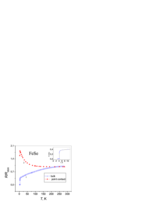
In Fig. 2, over a wide temperature range, we demonstrate the difference between the dependencies of the resistance of the bulk FeSe sample on the carriers energy set by the temperature T, derived from the conventional four-probe measurement geometry, and the same dependencies for point-contact samples Cu/FeSe with oxide barriers at the interface obtained in the measurement geometry of combined probes shown in Fig. 1 a, b. We see that the difference is qualitative: The character of the formers corresponds to the metallic behavior while that of the latters is semiconducting. In all the samples with FeSe, both bulk and hybrid, the superconducting transition was observed in the range of K (see Inset). In general, the above features of the temperature behavior are also characteristic of both bulk and hybrid NS samples with LaO(F)FeAs which experiences a superconducting transition at K.
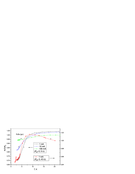
Figs. 3 and 4 show typical temperature dependencies of the normalized resistance of point contacts Cu/FeSe and Cu/LaO(F)FeAs measured at different transport currents. It is seen that, while increasing measuring current in the studied range mA, the share of a normal part of the point-contact system is increasing while that of a superconducting part corresponding to the change in the contact resistance at the superconducting transition is decreasing. The absolute value of the superconducting jump in resistance is the same for contacts with different total resistances but measured at the same current [compare curves 1 () and 2 () in Fig. 3]. This indicates that the interface resistance in the samples with pressed point contacts, in addition to the temperature-dependent semiconductor-type part, contains a temperature-independent part of the type of residual resistance which does not vanish at .
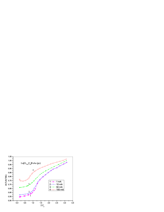
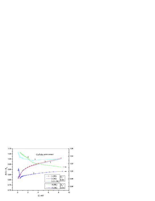
In Fig. 5, presented are the dependencies of the resistance for the system Cu/FeSe on the bias voltage U at the contact as an addition to the energy . Applying that voltage is an alternative method of controlling energy of the carriers. Curves 1, 2, and 5 correspond to the temperature range covering the area of the superconducting transition (, NS mode) while curves 3 and 4 were taken in the same interval of bias voltages at temperatures (NN mode). It is seen that in comparable energy ranges, the resistance behavior depending on the parameters T (Figs. 2, 3) and U (Fig. 5) is qualitatively similar in both NN and NS interface modes, the values of contact resistance in the NN mode differing by an order of magnitude. From this and from a comparison between curve 2 in Fig. 2 and curves 3 and 4 in Fig. 5, an important conclusion follows that in the energy range supporting heterocontacts in NN mode, the semiconductor type of behavior of the generalized contact conductance most likely is due to the energy-dependent dissipative contribution from the oxide layer, as the conductivity of FeSe over the entire temperature range above has a metallic behavior (Fig. 2, curve 1) while the resistance of the part of the copper probe included in the measurement, as small as m in length, cannot exceed a few at liquid helium temperatures. The theory predicts [18] that the proximity effect in "dirty" conductors extends to a depth proportional to the electron mean free path. Hence, at typical thickness of the "dirty" oxide layers Å, the electron mean free path in them is apparently of the same order. In other words, the residual resistance of contacts in NS state below the superconducting transition is formed by the intrinsic contribution from the interface () which is not associated either with oxide layers or with the N-side of the interface. As can be seen from Figs. 3, 4, and 5, for different contacts amounts to () % of the normalizing resistance measured in NN mode just before the superconducting transition. Most likely, reflects the presence in the heterojunction of a potential barrier of the Schottky type, or the contribution from surface localized states, or both.
We believe that all these features of the experimental data are directly related to the proximity effect associated with the dispersion of the order parameter which is especially significant in the range of T not too far from , where its spatial scale defined by the Ginsburg-Landau coherence length , is quite large. This can be seen by comparing the magnetic energy W of tangential self-magnetic field of the current Oe at the penetration depth with the potential of electron pairing . The notations are as follows: r is the radius of the channel, x is the coordinate measured from the interface on the side of a superconductor occupying a half-space and are the Fermi velocity and the correlation length. The estimation by the formulae of phenomenological theory [18] leads to the following result:
| (1) |
[in the interval , we replaced the distribution by = const; is the interface area ()]. Thus, for a current of 1 mA, with a typical for London superconductors m, the energy of the self-magnetic field of the current amounts to meV, while the value of is just meV. (Note, incidentally, that indicated strength of this inequality for currents greater than 1 mA is also preserved for Pippard superconductors with m.) Thus, the examined current interval is suitable for the manifestation of the effect discussed. Moreover, the fact that the current self-field at mA can eliminate the manifestation of the superconducting transition, either almost completely for FeSe (Fig. 3, curve 4) or significantly for LaO(F)FeAs (Fig. 4, curve 4), means the following. First, the Ginsburg-Landau parameter and hence discussed superconductors, must be characteristic of the London type-II superconductors and, second, the thickness of the superconducting part of the contacts is of order of the London penetration depth m [18]. It follows that the length of the measured contact area is of the order of a micron or slightly more - the typical mesoscopic size which turns out to be non-ballistic due to the presence of the areas with even shorter elastic mean free paths of electrons and because of the contact geometry characterized by combined current and potential probes [16].
Inequality (1), of course, overstates the requirements for the value of needed to suppress superconductivity in the range of , since it implies to be constant over the whole length of the interval. However, as noted above, the suppression should be also implemented at lower values of the field at a spatial scale of , due to the dispersion of the order parameter in the proximity effect area. Indeed, the distribution of the magnetic energy in the superconductor side () depends on the law of magnetic field distribution along the length of the penetration depth; according to the phenomenological theory [18], it can be written as
| (2) |
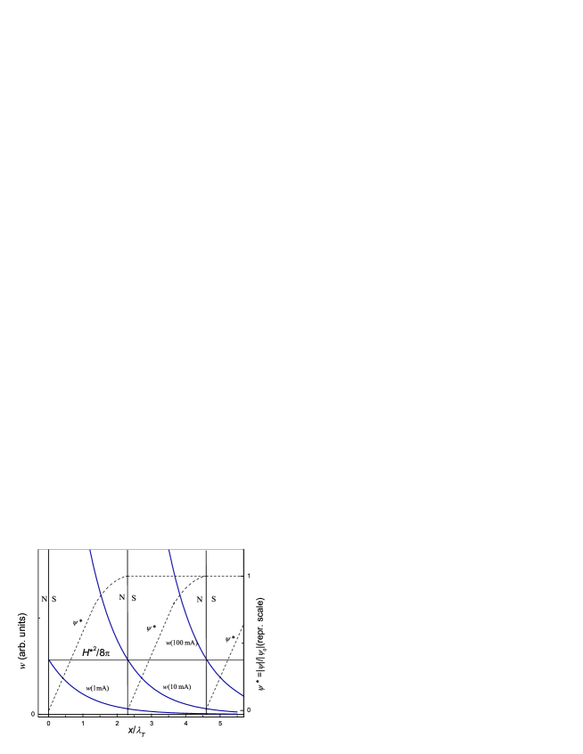
Let is the lowest field, energy density of which is comparable in value to the reduced, due to the proximity effect, value of normalized to a volume unit. Then, the suppression of superconductivity at arbitrary will extend to a depth of x depending on , ie, on the transport current value , up to that value of x at which one reaches . For larger x, ie, for , the superconducting state persists. Thus, the value of sets the position of a defect-free NS boundary between normal and superconducting parts of the superconductor. From this point, let us analyze, for example, the data depicted in Fig. 3. From a comparison of Eq. (2) for two values of it follows
| (3) |
where i, k = 1 mA, 10 mA, or 100 mA; . From the system of pairwise equations we find
| (4) | |||||
Here, the displacement of the boundary is measured relative to its position at which position, as shown by measurements at mA (see below), is very close to the starting point x = 0 in the absence of current. Based on Eqs. (4), Fig. 6 explains the physics of this effect that would be impossible in the absence of the proximity effect in the fields the maximum value of which, as we have, does not exceed Oe. For FeSe, for example, that value is more than an order of magnitude lower than that of the first critical field [21].
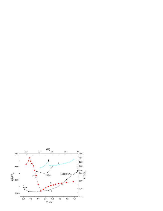
The possibility to get a defect-free NS boundary inside a superconductor allows us to interpret with reasonable certainty the effects associated with converting the dissipative current into supercurrent through the mechanism of Andreev reflection. On temperature dependencies measured at mA for Cu/FeSe (Fig. 3, curve 2) and at mA for Cu/LaO(F)FeAs (Fig. 4, curve 4) as well as on bias-voltage dependencies for Cu/FeSe (Fig. 5, curve 5), gap features are clearly visible. These are positive jumps in the contact resistance at the transition from the NN to NS regime which value amounts to around 2-3 % (with resolution better than 0.1 %) relative to the resistance before the superconducting transition. Similar feature is barely visible on curve 1, Fig. 5, while controlling the energy by bias voltage U. It can be easily understood by noting that under conditions where most of the energy of the electrons is set by the temperature, an addition required for the realization of a gap peculiarity is too small at K and for low-resistance sample (); besides, in a constant-current mode (see above), the current itself is small. Indeed, the area of the feature controlled by bias voltage at 3 K (curve 1, Fig. 5) corresponds to the current of order of 0.04 mA, while that current at 2 K (curve 5, Fig. 5) amounts to around 0.5 mA. Thus, it is of the same order as the current 1 mA which value corresponds to the discussed jump in resistance controlled by temperature in the contacts Cu/FeSe with the resistance greater by almost an order of magnitude (. This should mean that the self-field of the current 0.04 mA is too small to invade into a dispersion region of the order parameter on the FeSe side in NS-interface mode, while at mA, the NS boundary is already shifted deep into the superconductor and thus presents an ideal boundary between normal and superconducting parts of FeSe at which the conversion of the dissipative current into non-dissipative one takes place. In contacts Cu/LaO(F)FeAs, this specific feature manifests itself only at the current mA, probably due to too low value of at 4.2 K where .
In NS systems with non-magnetic superconductors, gap features in the conductance upon Andreev reflection can occur because of the coherent scattering by impurities on the normal side of the interface [17, 13] [we recall that we have included the relevant contribution to the resistance from this effect into the total resistance of the contact N-side and denoted it by (i), see Sec. 1]. In systems with magnetic superconductors, a decrease in the conductance of a contact [contribution (iii)] at the transition to a sub-gap energy region should also occur as a consequence of the spin polarization of the current due to the limitation of the Andreev reflection process in the presence of the dispersion of the spin subbands related by magnetic exchange interaction [22]. As a result of these limitations, the accumulation of spin should occur at the interface [23, 24] accompanied by the appearance of a positive addition to the applied bias voltage which, given constant-current mode, manifests itself as an additive to the total resistance of the contact in the NS regime. We associate the features observed on the and dependencies shown in Figs. 3, 4, and 5 with this additive. From these figures it also follows that the residual resistance of the contacts in the NS regime, particularly at the current of 1 mA, is by several orders of magnitude greater than the possible coherent effect of increasing in the resistance in the normal region of the probe as already noted for the systems in the same situation [16]. This allows us to attribute the observed features to the manifestation of only the spin accumulation effect. As a direct consequence of the spin polarization, the effect thus gives an indication of the magnetic characteristics of a superconductor in the normal ground state which is implemented in a finite region of NS heterojunction due to the proximity effect.
Fig. 7 shows an enlarged view of these features depending on both control parameters, temperature and bias voltage, for the contacts with FeSe and on temperature for the contact with LaO(F)FeAs. Previously, we observed the effect of spin accumulation in the systems "ferromagnet-superconductor" Fe/In and Ni/In where its value reached 20 % and 40 %, with degree of spin polarization of 45 % and 50 %, respectively [25]. Recall that the nature of the effect in the NS systems with conventional ferromagnets is associated with the destruction of the symmetry with respect to spin rotation which imposes limitations on the probability of Andreev reflection and results from high internal magnetic field that manifests itself in the spontaneous magnetization. Manifestation of spin accumulation in unconventional superconductors in normal ground state also points to the absence of such symmetry, but it cannot be associated with the bulk magnetization, for the latter, in our opinion, is not compatible with superconductivity at the microscopic level. Thus, once again we get the arguments in favor of that the magnetism of iron-based superconductors is limited by band magnetism of conduction electrons, for example, of the type of antiferromagnetic exchange interaction [26].
Knowing the magnitude of the effect of spin accumulation indicating the presence of spin polarization of the conduction electrons in the normal ground state of FeSe (strictly speaking, of the superconducting phase of FeSe in the normal state which can amount to as low as 15 % [26]), we estimate the polarization factor of the current P in studied contacts with single-crystal FeSe. According to the theory [23, 24], corresponding normalized additive to the resistance of the spin-polarized area due to spin accumulation is of the scale
| (5) | |||||
Here, are the total and spin-dependent conductivities; is the spin relaxation length; is the cross section of NS boundary (of the contact). As , we take the total resistance of the superconducting phase of the sample in the normal state equal to the value of the resistive jump at the superconducting transition, assuming that the length of the spin relaxation is of order of the dimension of this phase, L, and the whole area in the normal state is completely spin-polarized. Then
| (6) |
Substituting the experimental values of (from curve 2, Fig. 3), cm (from independent measurement by a standard four-probe method), cm, and cm2, we get %. We shall verify that this value corresponds to that ratio of spin-dependent conductivities at which a negative correction can exist to the conductance of spin-polarized ferromagnetic area (F) at the transition from the F/F to F/S regime. To do this, we use the estimates from Ref. [22] which establish the sign criterion for the resistive addition at a similar transition. The estimates are based on the arguments that the electrons retroreflected as Andreev holes must double their contribution to the conductance since at each reflection, a charge 2e is transferred. Here, however, the possibility of limiting the effect is not included due to doubling the cross section of subsequent coherent scattering by impurities in non-ballistic samples with short mean free path, as noted above. Expressing the ratio of spin-dependent conductivities in polarization we get this criterion in the form:
| (7) |
Our experimental situation is entirely equivalent to the first case: .
The estimate of the polarization for granular material LaO(F)FeAs by the same method (from curves 1 and 4, Fig. 4) gives a value of % which is in contradiction with the criterion (7). This again suggests that the physics of conductivity of granular compounds is much more complicated than that of single-crystal ones, in particular, because of the network of intergranular connections.
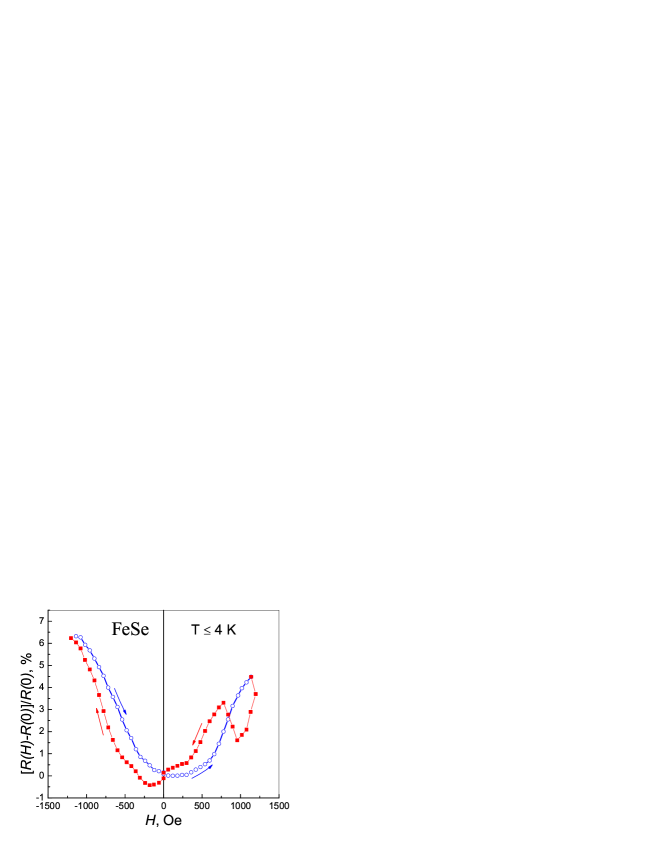
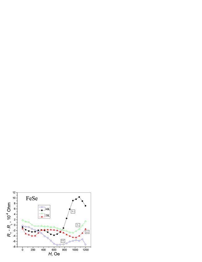
In addition to probable itinerant magnetism, we have tested the concept of spin-polarized conductivity of FeSe for the possibility that an alternative type of magnetism exists which is characterized by residual magnetization at reverse magnetizing. To do this, we measured the conductance of the normal part of FeSe within boundaries defined, as a reasonable belief, by the proximity effect, in an external magnetic field, a lot of smaller values in comparison with those converting the order parameter to unity. The measurements show that the hysteresis of magnetoresistance does not contain an irreversible effect at H = 0 for any sequence of magnetizing, as can be seen from the form of the magnetoresistance hysteresis curves shown in Fig. 8. Besides, other characteristic features of hysteresis strike the eye (see Fig. 9): (a) The branches belonging to different magnetic field directions are asymmetric and (b) the vertical displacement of the hysteresis branches in the fields exceeding the first critical field Oe [21] is of the same order of magnitude as the gap features in Fig. 7. These features of the hysteresis are, of course, directly related to the spin polarization of the current, and the absence of residual magnetoresistance at for all sequences of magnetizing shows that the nature of superconductivity in layered superconductors is associated with the magnetism of conduction electrons (itinerant magnetism) which does not interfere with the local magnetism of magnetic ions (such as iron ion). Note that the hysteresis of magnetoresistance was usually observed in granular systems, but in contrast to our results obtained in a single-crystal FeSe, it contained non-reversible values of the resistance during reversible magnetizing. This gave rise to interpret its nature in terms of percolation mechanism of current flow along the network of Josephson junctions [27]. The data from our single-crystal samples of FeSe rejecting such a possibility are closest to a vortex scenario of hysteresis which is based on the dissipative mechanism of synchronizing the vortices in the presence of defects [28].
4 Conclusion
We have investigated the electron transport through a barrier-free NS boundary set by the proximity effect and the transport current inside unconventional iron-based superconductors, single-crystal chalcogenide FeSe and granular oxypnictide LaO(F)FeAs, as parts of heterocontact samples of mesoscopic scale.
The evidence for the spin polarization of electron transport is obtained based on the sensitivity of Andreev conductance to symmetry with respect to the spin rotation.
The nature of the hysteresis of magnetoresistance observed in the fields much less in value than that of the second critical field, under dispersion of the order parameter, also points to the spin polarization of the charge carriers.
The results suggest that the nature of superconductivity in layered superconductors is connected with the magnetism of conduction electrons (itinerant magnetism) which has nothing in common with the local magnetism of iron ions.
References
- [1] Y. Kamihara et al., J. Am. Chem. Soc. 128, 10012 (2006).
- [2] F.-C. Hsu et al., arXiv:0807.2369 (2008).
- [3] Y. Mizuguchi et al., Appl. Phys. Lett., 93, 152505 (2008).
- [4] A. Subedi, L. Zhang, D.J. Singh, and M.H. Du, Phys. Rev.B 78, 134514 (2008).
- [5] D.J. Singh and M.H. Du, Phys. Rev. Lett. 100, 237003 (2008).
- [6] A. Chubukov, Ann. Rev. Cond. Matt. Phys. 3, 57 (2012).
- [7] D.J. Singh and M.-H. Du, Phys. Rev. Lett. 100, 237003 (2008).
- [8] M.J. Han and S.Y. Savrasov, Phys. Rev. Lett. 103, 067001 (2009).
- [9] W.L. McMillan, Phys. Rev. 167, 331 (1968).
- [10] Z.P. Yin et al., Phys. Rev. Lett. 101, 047001 (2008).
- [11] P.P. Singh, Phys. Rev. Lett. 104, 099701 (2010).
- [12] M.J. Han and S.Y. Savrasov, Phys. Rev. Lett. 104, 099702 (2010).
- [13] Y.N. Chiang (Tszyan), in: A.M. Luis (Ed.), Superconductivity. Theory and Applications, InTech, Croatia, 2011, pp. 99–128 (Chapter VI).
- [14] Yu.V. Sharvin, Sov. Phys. JETP 21, 655 (1965).
- [15] G.E. Blonder, M. Tinkham, and T.M. Klapwijk, Phys. Rev. B 25 4515 (1982).
- [16] Yu.N. Chiang, M.O. Dzyuba, O.G. Shevchenko, A.N. Vasiliev, Physica C 483, 149 (2012).
- [17] J.Herath and D. Rainer, Physica C 161, 209 (1989); A.M. Kadigrobov, Low Temp. Phys. 19, 671 (1993).
- [18] P.G. De Gennes, Superconductivity of Metals and Alloys (W.A. Benjamin, INC. New York - Amsterdam, 1966).
- [19] X. Zhu, H. Yang, L. Fang, G. Mu, and H.-H. Wen, Supercond. Sci. Technol. 21, 105001 (2008).
- [20] G.Hägg and A. L. Kindstrom, Z. Phys. Chem. 22, 455 (1933).
- [21] P. K. Biswas, et al., arXiv:1209.5279 (2012).
- [22] M.J.M. de Jong and C.W.J. Beenakker, Phys. Rev. Lett. 74, 1657 (1995).
- [23] V.I. Fal’ko, A.F. Volkov, and C.J. Lambert, JETP Lett. 69, 532 (1999).
- [24] F.J. Jedema, B.J. van Wees, B.H. Hoving, A.T. Filip, and T.M. Klapwijk, Phys. Rev. B 60, 16549 (1999).
- [25] Yu.N. Chiang, O.G. Shevchenko, and R. N. Kolenov, Low Temp. Phys. 33, 314 (2007).
- [26] C. Zener, Phys. Rev. 82, 403 (1951).
- [27] T.V. Sukhareva and V.A. Finkel’, Phys. of Solid State 50, 1001 (2008).
- [28] E. Altshuler, S. Garcia, J. Barroso, Physica C 177, 61 (1991).