Graphene-coated holey metal films: tunable molecular sensing
by surface
plasmon resonance
Abstract
We report on the enhancement of surface plasmon resonances in a holey
bidimensional grating of subwavelength size, drilled in a gold thin film
coated by a graphene sheet. The enhancement originates from the coupling
between charge carriers in graphene and gold surface plasmons. The main
plasmon resonance peak is located around m. A lower constraint on the gold-induced doping
concentration of graphene is specified and the interest of this
architecture for molecular sensing is also highlighted.
†These authors contributed equally to this work.
pacs:
78.67.Wj, 73.20.Mf, 42.79.Dj, 07.07.DfPlasmonic devices offer valuable platforms for a wide range of emerging molecular detection schemes. Among such applications, biosensors are very promising especially from the point of view of lab-on-a-chip (LOC) technologies.LOC Indeed, plasmon resonances are characterized by both a strong electric field and a great sensitivity to environmental conditions. As a consequence, adsorbed species can be detected through the resonance wavelength shift. In addition, the strong electric field enhancement allows for surface enhanced Raman spectroscopy, which can be used for single molecule detection.sers
Surface plasmons (SPs) require specific conditions to be excited. For instance, in the Kretschmann configuration, a light beam is totally internally reflected in a prism on which a metallic film is deposited and triggers the generation of SPs.Raether In a holey metal film, SPs can be excited by a normal incidence light beam.Ebbesen Light is scattered due to the corrugations and the evanescent diffraction orders can excite SPs.Wood For a metallic layer accommodating an array of holes with subwavelength size, it is possible to probe SPs by simply measuring the intensity of the transmitted light. Such a simple configuration is much more practical in the LOC context and it has been widely studied since the pioneering work of Ebbesen et al. in 1998.Ebbesen
Recent theoretical works have shown that doping can induce SP modes in graphene.Jablan ; Abedinpour ; Koppens Graphene, which appears as a monoatomic layer made of sp2 carbon atoms in a hexagonal lattice configuration, presents a plethora of amazing properties.Geim In that context, SPs have been observed for graphene doped by charge transfer from metal thin films,Salihoglu ; Khomyakov ; Giovannetti ; Fang external atoms Shin or electrostatic gating Chen ; Fei . It has been also suggested that SPs could be excited in graphene on a periodically structured substrate Zhu ; Ferreira or via regular patterns in graphene.Bludov ; Nikitin1 ; Nikitin2 ; Nikitin3 ; Popov1 ; Popov2 ; Thongrattanasiri A recent experimental result showed that graphene SPs can be excited in a Kretschmann configuration using graphene deposited on a planar gold layer.Salihoglu A different approach Niu was used in which SP resonance tunability was achieved by electromagnetic field coupling between a graphene sheet and SPs excited in gold nanoparticles.
In the present work, we describe and study an optical device constituted by a planar hexagonal array of subwavelength-sized holes in a gold thin film functionalized with a graphene layer. The entire device is built on a glass substrate. Resonances of the device are measured for various incidence angles. It is shown that graphene enhances the plasmon resonances and induces a redshift of the resonance wavelength. This plasmonic device used as a molecular sensor displays a wavelength shift which is highly sensitive to environmental conditions.
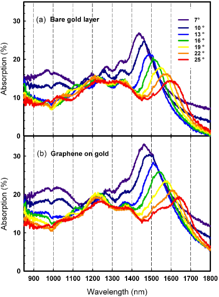
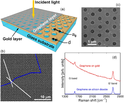
Figure 1(a) gives a conceptual illustration of the nanostructured plasmonic platform. It was fabricated by using colloidal nanosphere lithography. Briefly, polystyrene spheres ( nm in diameter, Microparticles GmbH) were deposited on soda-lime glass plates via an interfacial self-assembly protocol.vlad1 ; vlad2 Reactive ion etching using O2 chemistry (Oxford Plasmalab, W RF power, sccm O2, mTorr, min) was used to reduce the size of the colloids to half the nominal diameter. Subsequently, nm of Ti followed by nm of Au were deposited using physical vapor deposition. The liftoff was performed using adhesive tape and ultrasonication in dichloromethane. Figure 1(b) shows a Scanning Electron Microscopy (SEM) top view of the array made of large periodic crystal-like domains.
Graphene was synthesized by atmospheric pressure chemical vapor deposition at 1000 ∘C on copper foils with methane as carbon source.Li ; Wu ; Reck The copper foil was inserted into a quartz reactor inside a hot-wall furnace. After annealing at 1000 ∘C for 30 min under argon (500 ml/min) and hydrogen (100 ml/min), methane was admitted (0.5 ml/min) for 15 min to grow graphene. It was next cooled down rapidly under argon and hydrogen. After spin-coating a polymethyl methacrylate (PMMA) film over graphene,dep the copper foil was etched in aqueous ammonium persulfate. Next, the PMMA/graphene stack was rinsed in distilled water and transferred onto the holey gold/glass substrate. The PMMA film was then removed by soaking into acetone and finally blown dry with nitrogen. Figure 1(c) shows a SEM top view of the resulting device. In addition, a reference sample with graphene over planar gold was fabricated. Graphene was also transferred on silicon dioxide (-nm-thick) for Raman inspection. The detection of G (1590 cm-1) and G′ (2690 cm-1) bands testifies of the presence of graphene (see the Raman spectra in Fig. 1(d), for graphene over planar gold and silicon dioxide). No disorder-related D band (1350 cm-1) is observed, suggestive of virtually defect-free graphene.
Optical characterization was carried out at various incidence angles by using an integrating sphere setup mounted on a Perkin-Elmer Lambda 750S UV/Vis/NIR spectrophotometer. The sample was positioned such that the light source faces the graphene surface at normal incidence. Figure 2(a) shows the absorption () of the bare holey gold film (i.e. without graphene). The extinction of the graphene-coated holey gold film is shown in Fig. 2(b) (). The typical absorption peaks denote surface plasmon polaritons.Wood As it can be observed, graphene induces a redshift of the plasmon resonance peaks and dramatically enhances the absorption of the device up to (see also Fig. 3(a)). It is noteworthy that the main plasmon resonance peak is located around m, close to the wavelength range of interest to optoelectronic applications.
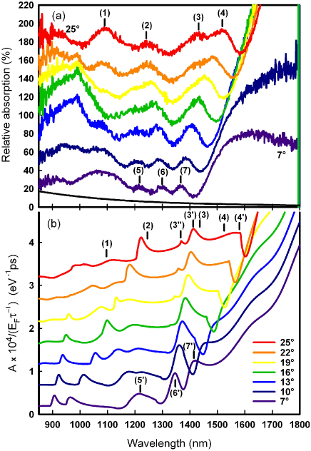
The relative absorption , calculated as , is shown in Fig. 3(a). The role of SPs is anticipated from the relative shift of the peaks in Fig. 3(a) for the considered incidence angles. In addition, the relative absorption of a graphene layer deposited on unstructured gold (black curve in Fig. 3(a)) shows a weak enhancement by contrast with the corrugated gold film. Since corrugated metallic films allow for SP modes, it is a strong argument for the coupling between SPs on gold and graphene. To further support this, we have run numerical simulations based on a homemade code which rests on a rigorous coupled wave analysis (RCWA) method.Wood By considering the frequency and position dependence of the electric field inside a given material, the absorbed power is given by:Jackson
| (1) |
where is the vacuum permittivity, is the imaginary part of the relative permittivity of the medium (here the graphene layer), and its volume. This formula can be expressed according to the real part of the medium conductivity, i.e. . For a two-dimensional-like medium, such as graphene, we get
| (2) |
with the surface, the position vector along the graphene layer, and where is the real part of the graphene conductivity. Mermin ; Hanson can be restricted to the intraband term:Hanson ; Hanson2 ; Jablan
| (3) |
with the reduced Planck constant, the electron charge, the Fermi level, and the relaxation time. The intraband approximation is legitimate since no resonance occurs below nm, suggesting that eV,Bludov ; Hanson2 corresponding to a charge density 4 cm-2.Jablan Albeit large, these values are in agreement with those achieved in other works.Khomyakov ; Giovannetti ; Shin
Let us now consider as the electric field of the electromagnetic wave scattered at the air/gold interface without graphene. We suppose that such an electromagnetic field is not significantly modified by the graphene layer as a first approximation. In addition, we suppose that the extrinsic conductivity of graphene due to the gold film can be considered as uniform, i.e. does not depend on . The incident power is given by , where is the speed of light, is the area of the unit cell of the array, and the electric field amplitude of the incident wave. Then, the absorption of graphene is defined as , and assuming that we work at frequencies , we get
| (4) |
where is the wavelength () and . Except for , which is a mere factor of proportionality, can be easily computed numerically using our homemade RCWA code, allowing to propagate the electromagnetic field on a bare perforated gold layer on glass. The permittivities of materials are taken from the literature.Palik In Fig. 3(b), we display the calculated quantity for different incidence angles. Markers (noted as numerals, from to , from to , and ) have been added in Figs. 3(a) and 3(b) for comparison. The global pattern in Fig. 3(b) matches very well the experimental data shown in Fig. 3(a). This supports the supposition that the enhancement is due to graphene conductivity coupled with surface modes, i.e. SPs at the gold/air interface. We note a few discrepancies, for instance, the peak at wavelength seems to result from two shifted resonances at wavelengths and Peaks at wavelengths to also appear shifted to wavelengths to . These differences between experiment and numerical simulations are due to the fact that we consider a perfectly periodic hole array in our simulation while the real one is constituted of a set of many crystal-like domains (see the SEM picture in Fig. 1(b)). In addition, the retroactive role of the graphene layer on the electric field is not considered. The present theoretical results indicate that graphene must be doped in order to support SPs (here, the doping is extrinsic and provided by the gold layer). Indeed, if (i.e. absence of doping) there is no absorption. In addition, the intraband approximation is also supported by the fact that the interband term Hanson ; Hanson2 is unable to reproduce the experimental patterns shown in Fig. 3(a).
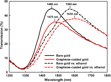
In the following, we show that graphene-coated holey gold films enhance the wavelength shift against the environment changes proving the versatility of this configuration for LOC sensing applications. We have analyzed the response of the devices in the presence of ethanol at the main plasmon resonance around m. Ethanol is first spread on the graphene side of the device. To avoid thin film interferences due to a thick ethanol layer, a delay of 30 seconds is set to allow ethanol to partially evaporate. This preserves an adsorbed layer with a subwavelength thickness. Transmission is then recorded. Figure 4 displays the response of the devices when in presence of ethanol. The zeroth order transmissions at normal incidence are plotted where a typical peak is observed for wavelengths around a SP resonance.Wood The transmission peak for both types of gold samples (graphene-coated and bare) is redshifted when exposed to ethanol. However, the graphene-coated sample shows a higher wavelength-shift sensitivity the resonance peak shift being greater than for the bare device. After complete evaporation of ethanol, the peaks retrieve their initial position. Note that the wavelength shift as well as the transmission decrease (i.e. the absorption enhancement) are related. Indeed, the surface plasmon wave vector must verify , where is the parallel component of the wave vector of the incident light wave with respect to the interface, and is a vector of the reciprocal lattice. For the smallest non trivial vector and for normal incidence, the wavelength for which a plasmon resonance occurs can be roughly approximated by:Jackson ; Raether
| (5) |
where is the permittivity of the dielectric environment which surrounds the metallic layer and the conductivity of the dielectric, which depends on the graphene layer conductivity. If increases, the optical absorption increases (since ), but is also shifted. Moreover, the ethanol layer present on the device alters the combined permittivity and also causes shift and intensity changes.
In summary, nanostructured hybrid graphene-gold architectures enhance the wavelength shift in plasmonic sensors. The simple graphene-coated metal grating device allows for a facile optical characterization at normal incidence, without the need of a complex Kretschmann configuration, greatly improving the portability of the measurement setup. Moreover, the rich graphene surface chemistry offers unique functionalization protocols, enlarging further the sensor’s versatility.Gao
The authors acknowledge C. N. Santos and B. Hackens for their help with Raman measurements, as well as F. J. Garcia de Abajo and L. Henrard for useful discussions and comments. This work was supported by the Belgian Fund for Scientific Research (F.R.S.-FNRS) under the FRFC contract ”Chemographene” (convention No.2.4577.11) and via the FRFC project No.2.4510.11. A.V., S.M. and J.-F.C. acknowledge F.R.S.-FNRS for financial support. This research used resources of the Interuniversity Scientific Computing Facility located at the University of Namur, Belgium, which is supported by the F.R.S.-FNRS under the convention No.2.4617.07.
References
- (1) H. Craighead, Nature 442, 387 (2006).
- (2) M. Moskovits, Rev. Mod. Phys. 57, 783 (1985).
- (3) H. Raether, Surface Plasmons on Smooth and Rough Surfaces and on Gratings (Springer-Verlag, Berlin and Heidelberg, 1988).
- (4) T. W. Ebbesen, H. J. Lezec, H. F. Ghaemi, T. Thio, and P. A. Wolff, Nature 391, 667 (1998).
- (5) M. Sarrazin, J.-P. Vigneron, and J.-M. Vigoureux, Phys. Rev. B 67, 085415 (2003).
- (6) S. H. Abedinpour, G. Vignale, A. Principi, M. Polini, W.-K. Tse, and A. H. MacDonald, Phys. Rev. B 84, 045429 (2011).
- (7) M. Jablan, H. Buljan, and M. Soljacic, Phys. Rev. B 80, 245435 (2009).
- (8) F. H. L. Koppens, D. E. Chang, and F. J. Garcia de Abajo, Nano Lett. 11, 3370 (2011).
- (9) A. K. Geim and K. S. Novoselov, Nature Mater. 6, 183 (2007).
- (10) O. Salihoglu, S. Balci, and C. Kocabas, Appl. Phys. Lett. 100, 213110 (2012).
- (11) P. A. Khomyakov, G. Giovannetti, P. C. Rusu, G. Brocks, J. van den Brink, and P. J. Kelly, Phys. Rev. B 79, 195425 (2009).
- (12) G. Giovannetti, P. A. Khomyakov, G. Brocks, V. M. Karpan, J. van den Brink, and P. J. Kelly, Phys. Rev. Lett. 101, 026803 (2008).
- (13) Z. Fang, Y. Wang, Z. Liu, A. Schlather, P. M. Ajayan, F. H. L. Koppens, P. Nordlander, and N. J. Halas, ACS Nano 6, 10222 (2012).
- (14) S. Y. Shin, N. D. Kim, J. G. Kim, K. S. Kim, D. Y. Noh, Kwang S. Kim, and J. W. Chung, Appl. Phys. Lett. 99, 082110 (2011).
- (15) J. Chen, M. Badioli, P. Alonso-Gonzalez, S. Thongrattanasiri, F. Huth, J. Osmond, M. Spasenovic, A. Centeno, A. Pesquera, P. Godignon, et al., Nature 487, 77 (2012).
- (16) Z. Fei, A. S. Rodin, G. O. Andreev, W. Bao, A. S. McLeod, M. Wagner, L. M. Zhang, Z. Zhao, M. Thiemens, G. Dominguez, et al., Nature 487, 82 (2012).
- (17) X. Zhu, W. Yan, P. U. Jepsen, O. Hansen, N. A. Mortensen, and S. Xiao, Appl. Phys. Lett. 102, 131101 (2013).
- (18) A. Ferreira and N. M. R. Peres, Phys. Rev. B 86, 205401 (2012).
- (19) Yu. V. Bludov, A. Ferreira, N. M. R. Peres, and M. I. Vasilevskiy, Int. J. Mod. Phys. B 27 1341001 (2013).
- (20) A. Yu. Nikitin, F. Guinea, F. J. Garcia-Vidal, and L. Martin-Moreno, Phys. Rev. B 84, 161407(R) (2011).
- (21) A. Yu. Nikitin, F. Guinea, F. J. Garcia-Vidal, and L. Martin-Moreno, Phys. Rev. B 85, 081405(R) (2012).
- (22) A. Yu. Nikitin, F. Guinea, and L. Martin-Moreno, Appl. Phys. Lett. 101, 151119 (2012).
- (23) V. V. Popov, T. Yu. Bagaeva, T. Otsuji, and V. Ryzhii, Phys. Rev. B 81, 073404 (2010).
- (24) V. V. Popov, O. V. Polischuk, A. R. Davoyan, V. Ryzhii, T. Otsuji, and M. S. Shur, Phys. Rev. B 86, 195437 (2012).
- (25) S. Thongrattanasiri, F. H. L. Koppens, and F. J. Garcia de Abajo, Phys. Rev. Lett. 108, 047401 (2012).
- (26) J. Niu, Y. J. Shin, Y. Lee, J.-H. Ahn, and H. Yang, Appl. Phys. Lett. 100, 061116 (2012).
- (27) A. Vlad, A. Frölich, T. Zebrowski, C. A. Duţu, K. Busch, S. Melinte, M. Wegener, and I. Huynen, Adv. Funct. Mater. 23, 1164 (2013).
- (28) A. Vlad, I. Huynen, and S. Melinte, Nanotechnology 23, 285708 (2012).
- (29) X. Li, W. Cai, J. An, S. Kim, J. Nah, D. Yang, R. Piner, A. Velamakanni, I. Jung, E. Tutuc, et al., Science 324, 1312 (2009).
- (30) B. Wu, D. Geng, Y. Guo, L. Huang, Y. Xue, J. Zheng, J. Chen, G. Yu, Y. Liu, L. Jiang, and W. Hu, Adv. Mater. 23, 3522 (2011).
- (31) N. Reckinger, A. Felten, C. N. Santos, B. Hackens, and J.-F. Colomer, arXiv:1303.3951 [cond-mat.mtrl-sci].
- (32) A. Reina, X. Jia, J. Ho, D. Nezich, H. Son, V. Bulovic, M. S. Dresselhaus, and J. Kong, Nano Lett. 9, 30 (2009).
- (33) J. D. Jackson, Classical Electrodynamics (Wiley, 1998).
- (34) N. W. Ashcroft and N. D. Mermin, Solid State Physics (Saunders, Philadelphia, PA, 1976).
- (35) G. W. Hanson, J. Appl. Phys. 104, 084314 (2008).
- (36) G. W. Hanson, J. Appl. Phys. 103, 064302 (2008).
- (37) E. D. Palik, Handbook of Optical Constants of Solids (Academic, Boston, 1985).
- (38) W. Gao, L. B. Alemany, L. Ci, and P. M. Ajayan, Nature Chem. 1, 403 (2009).