Dynamic effects in double graphene-layer structures with inter-layer resonant-tunneling negative conductivity
Abstract
We study the dynamic effects in the double graphene-layer (GL) structures with the resonant-tunneling (RT) and the negative differential inter-GL conductivity. Using the developed model, which accounts for the excitation of self-consistent oscillations of the electron and hole densities and the ac electric field between GLs (plasma oscillations), we calculate the admittance of the double-GL RT structures as a function of the signal frequency and applied voltages, and the spectrum and increment/decrement of plasma oscillations. Our results show that the electron-hole plasma in the double-GL RT structures with realistic parameters is stable with respect to the self-excitation of plasma oscillations and aperiodic perturbations. The stability of the electron-hole plasma at the bias voltages corresponding to the inter-GL RT and strong nonlinearity of the RT current-voltage characteristics enable using the double-GL RT structures for detection of teraherz (THz) radiation. The excitation of plasma oscillations by the incoming THz radiation can result in a sharp resonant dependence of detector responsivity on radiation frequency and the bias voltage. Due to a strong nonlinearity of the current-voltage characteristics of the double-GL structures at RT and the resonant excitation of plasma oscillations, the maximum responsivity, , can markedly exceed the values V/W at room temperature.
I Introduction
As demonstrated recently 1 ; 2 ; 3 ; 4 , double graphene-layer (GL) structures with the inter-GL layers forming relatively narrow and low energy barriers for electrons or holes can be effectively used in novel devices. The excitation of plasma oscillations in these structures, i.e., the excitation of spatio-temporal variations of the electron and hole densities in GLs and the spatio-temporal variations of the self-consistent electric field between GLs, by incoming terahertz (THz) radiation, modulated optical radiation, or ultra-short optical pulses provides additional functional opportunities. In particular, the double-GL structures with the inter-GL tunneling or thermionic conductance can be used in the resonant THz detectors and photomixers 5 ; 6 . As was recently discussed 7 ; 8 ; 9 and realized experimentally 10 , the inter-GL resonant tunneling (RT) in the double-GL structures, with the band diagrams properly aligned by the applied voltage, leads to inter-GL negative differential conductivity (NDC) and enables novel transistor designs with the multi-valued current-voltage characteristics. A strong nonlinearity of the inter-GL current-voltage characteristics at the voltages near tunneling resonance can be used in double-GL-based frequency multipliers 8 , detectors 5 , and other microwave and THz devices. However, NDC might, in principle, result in the instability of stationary states, modifying or even harming normal operation of double-GL transistors and two-terminal devices.
In this paper, we consider the double-GL structures with tunneling transparent barrier layers exhibiting RT and NDC. Using the proposed model, we calculate the device admittance and demonstrate that a steady-state current flow in these structures is stable with respect to the self-excitation of plasma oscillations and aperiodic perturbations despite NDC. The incoming electromagnetic radiation, particularly, THz radiation can result in an effective resonant excitation of plasma oscillations, which can be used for the THz detection. We calculate the rectified current and the responsivity of the THz detectors based on the double-GL RT structures and show, that due to a strong nonlinearity of the double-GL current-voltage characteristics and the possibility of the resonant excitation of plasma oscillations by incoming THz radiation, the structures under consideration can serve as THz detectors exhibiting very high responsivity.
II Model equations
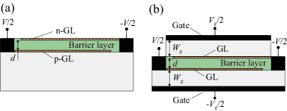
We consider the double-GL structures either with chemically doped GLs (figure 1(a)) or with undoped GLs but sandwiched between two highly conducting gates (figure 1(b)). In the first case, one of the GLs is doped by donors, whereas the other one is doped by acceptors, so that the electron and hole sheet densities in the pertinent GLs are equal tothe dopant density (donors and acceptors) . In the second case, the voltage applied between the gates, induces the electrons and holes with the sheet charge densities , where is the thickness of the layers separating GLs and the gates (see figure 1(b)).
Each GL is supplied by an Ohmic side contact (left-side contact to lower GL and right-side contact to upper GL) between which the bias voltage is applied. This voltage affects the electron and hole steady-state densities :
| (1) |
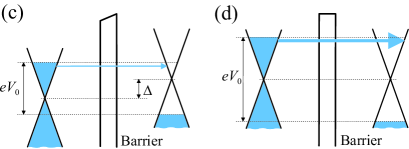
Here is the value of the electron charge, is the dielectric constant, and is the spacing between GL (i.e., the thickness of the inter-GL barrier). Figures 1(c) and 1(d) show the band diagrams of the double-GL structures under consideration at and , respectively. The energy difference, , between the Dirac points in GLs is determined by the following equation (see figure 1(c)):
| (2) |
where is the Fermi energy of electrons and holes in the pertinent GL. In practically interesting cases, the electron and hole systems in GLs are degenerated even at room temperatures. This occurs when is sufficiently large in comparison with the equilibrium density : , where and are the Planck and Boltzmann constants, respectively, cm/s is the characteristic velocity of electrons and holes in GLs, and is the temperature. In such a case,
| (3) |
Using equations (1) and (2) and the alignment condition , we obtain the following formula for the alignment voltage:
The local value of the inter-GL resonant-tunneling current density as a function of the bias voltage is given by 7 ; 8
| (5) |
where is the peak value of the current density and determines the peak width, is the coherence length (the characteristic size of the ordered areas in GLs).
Using equation (5) , at small signal variations of the local potential difference between GLs , the variation of the RT current density can be presented as
| (6) |
Here is the differential tunneling conductivity and determines the nonlinearity of the RT current-voltage characteristics:
| (7) |
| (8) |
As follows from equation (7), changes its sign at and becomes negative when . The maximum value of , which is achieved at , is equal to . Equation (8) for the value at yields .
The spatial distributions of and in the GL plane (along the axis ) can be found from linearized hydrodynamic equations (adopted for the energy spectra of the electrons and holes in GLs 12 ) coupled with the Poisson equation in the gradual channel approximation 13 . We limit our treatment to the in-phase perturbations of the electron and hole densities. For such perturbations, the self-consistent ac electric field is located between GLs. The difference in the local values of the ac potentials of the upper and lower GLs causes the inter-GL current, which can either increase or decrease with varying depending on the value of . For the out-off-phase perturbations of the electron and hole densities, the ac electric field is located mainly outside the double-GL structure, so that the inter-GL tunneling is insignificant and no effects associated with NDC can be expected.
Calculating the ac potentials, one can neglect the nonlinear component of the ac inter-GL current. i.e., the second term in the right-hand side of equation (6) (see, however, Sec. IV) and searching for the ac potential in the following form: , where is the complex signal frequency. In this case, the system of equations in question can be reduced to the equations for the ac components of the potential at the frequency 3 ; 4 :
| (9) |
| (10) |
Here is the collision frequency of electrons and holes in GLs with impurities and acoustic phonons and is the characteristic velocity of plasma waves in double-GL structures. Since electrons and holes belong to different GLs separated by a relatively high barrier, we have disregarded the electron-hole scattering and, hence, the effect of mutual electron-hole drag 12 . The characteristic velocity in the double-GL structures (similar to that in the two-dimensional electron or hole channels in the standard semiconductors with metal gates) is determined by the net dc electron and hole densities and the inter-GL layer thickness 14 ; 15 ; 16 ; 17 . In double-GL structures with the degenerate electron-hole plasma, , where is the ”fictitious” mass of electrons and holes in GLs. This implies that 14 . The value of in the GL structures under consideration can be fairly high, always exceeding the characteristic velocity of electrons and holes in GLs 14 ; 18 . Considering equations (6), (9), and (10), we obtain
| (11) |
| (12) |
Here is the characteristic frequency of the inter-GL tunneling. At , and , while at , and, hence .
Assuming that the total voltage between the contacts to GLs is equal to , where is the small signal voltage component, one can use the following boundary conditions for equations (11) and (12):
| (13) |
The latter boundary conditions reflect the fact that the electron and hole currents are equal to zero at the disconnected edges of GLs (at in the upper GL and at in the lower GL), while the difference of the ac potentials can generally be nonzero.
Solving equations (11) and (12) with boundary conditions (13), we obtain
| (14) |
where .
III Admittance of the double-GL resonant-tunneling structures
First, we calculate the small-signal admittance, of the double-GL RT structures, , where
| (15) |
is the net ac current, including the displacement current and is the width of the double-GL structure in the direction perpendicular to the currents. Using equations (14) and (15), we find
| (16) |
Here we have introduce the plasma frequency , so that . In the limit , equation (16) yields if . This implies that in this case the dc admittance is determined by the inter-GL conductivity. When , we find , where stands for the dc conductivity of GLs.
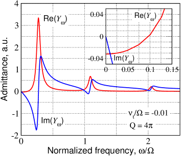
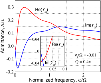
Figure 2 shows the frequency dependences of the real and imaginary parts of the admittance calculated using equation (16) for different values of the plasma oscillation quality factor ( and ) and . As seen, Re is negative in a narrow range of small frequencies. This is due to NDC at associated with RT. However, at higher signal frequencies, Re is positive. One can also see that Im does not change its sign in the frequency region, where Re . This implies that the electron-hole plasma is stable, at least for the chosen parameters. Indeed, the stability of stationary state of the electron-hole plasma at given bias voltage is determined using the condition . Considering the latter, we obtain the following condition for the damped or growing of perturbations of the electron and hole densities, i.e., the following dispersion equation for plasma oscillations:
| (17) |
Equation (17) determines the complex frequency , where is real value of possible plasma oscillations and is their damping/growth rate. For the structures with the characteristic plasma frequency , equation (17) yields , and , where
| (18) |
If , we find from equation (17)
| (19) |
The plasma frequency can vary in a wide range depending on the structure length . In particular, setting cm/s and m (as in Ref. 10 ), one obtains THz (so that according to equation (18) THz). But if m, one can get THz.
As follows from equations (18) and (19), the plasma instability (the increment, i.e,the growth rate ) is possible if in the structures with a high quality factor or in the structures with . In the former case, plasma oscillations with the frequencies can self-excite, while in latter case, the growth of the perturbations of the electron and hole densities is aperiodic, which could potentially result in the domain formation. In such situations, the stationary current flow between GLs could be unstable. However, in real double-GL structures the value of the differential inter-GL RT conductivity is not sufficiently large to provide the condition . To estimate the real value of , we assume that A/cm2 8 ; 9 ; 10 and nm, so that mV. This yields S/cm2. If nm and (hBN four atomic layers thick barrier), one obtains s As seen, at realistic s-1, the value . This is in contrast to the double-barrier RT devices based on InGaAs-AlAs, where the frequency can be rather high, being of the order of or even exceeding the electron collision frequency. This is due to a very high peak current density and modest width of the tunneling resonance in the double-barrier RT diodes. This can lead to the instability of the stationary current with respect to the self-excitation of plasma oscillations 19 . For instance, in one of the best resonant-tunneling diode 20 , , S/cm2 and nm, so that s.
In relatively long double-GL structures, inequality can be satisfied if the collision frequency is large and, hence, the mobility of electrons and holes is low. Indeed, setting THz and s-1, the latter inequality needs s-1. The latter condition is not met for the double-GL structures considered recently 8 ; 9 ; 10 .
IV Resonant detection of radiation
The ac potential between the contacts to GLs can arise due incoming electromagnetic radiation received by an antenna. This results in the excitation of plasma oscillations in the double-GL structure described by equation (14). The ac potential drop causes not only the linear component of the tunneling current but also the rectified dc current, , associated with the nonlinear (quadratic) component. The rectified ac current is given by the following formula:
| (20) |
This rectified component of the inter-GL RT current can be used for detection of THz signals. Using equations (14) and (20), we obtain the following formulae for the rectified current and the detector Volt-Watt responsivity
| (21) |
| (22) |
Here the characteristic responsivity is given by
| (23) |
where is the speed of light in vacuum, is the antenna gain factor, and are the inter-GL dc conductivity and current density, respectively. Considering that at (when the resonant-tunneling current exhibits a maximum) above expression yields , we arrive at the following formula
| (24) |
Equation (23) provides the frequency dependence similar to the responsivity of the double-GL detectors using the nonlinearity of the inter-GL relatively smooth current-voltage characteristic with the tunneling assisted by electron scattering (non-resonant tunneling detector) considered by us recently 5 . However, there are two distinctions (apart from the difference in the sign). First, the absolute value of is much larger than . This is due to a significantly larger value of in the RT detectors associated with a high and sharp RT peak. Indeed, considering equation (24) and the pertinent equation in 5 , one can arrive at
| (25) |
Setting mV and mV, we obtain . At the above parameters, assuming that , one obtains V/W. Second, the responsivity peaks of the inter-GL RT detector width is characterized by the collision frequency (because ), but in the detectors using non-resonant tunneling the width of the peaks is determined by with . The possibility to achieve very high values of the characteristic responsivity is connected with a large value of and, hence, small values of the width of tunneling resonance . One can assume that the latter quantity weakly depends on the temperature 8 , so that the responsivity can be very high even at room temperature.
As follows from equation (22), the frequency dependence of the responsivity exhibits sharp maxima at the plasma resonant frequencies , where the frequencies are given by equation (16). The widths of the peaks are determined by the parameter (at the RT resonance ). At the plasma resonances, . Thus, very high values of the responsivity of the detectors in question can be achieved due to combining of the tunneling and plasma resonances.
Since the resonant plasma frequencies fall into the THz range, the detector under consideration can be particularly useful for the resonant detection of THz radiation.
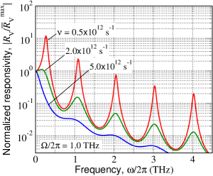
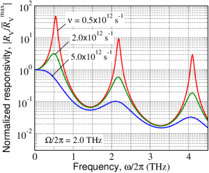
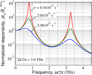
Figure 3 demonstrates examples of the frequency dependences of the responsivity calculated using equation (22) for the double-GL RT structures with different values of the electron and hole collision frequency and different values of the plasma frequency . The obtained dependences of the responsivity versus signal frequency exhibit several resonant peaks associated with the plasma oscillations. The highest peaks correspond to the zeroth resonances at the frequency , while the other resonances correspond to multiples of the plasma frequency (see equation (18)). One can see that not only at the zeroth plasma resonance, but also a higher resonances. The number of such resonances depends on the quality factor . The responsivity is very high due RT with sharp maximum at the current voltage-characteristics even at the moderate quality factors. However, it is much higher at the pronounced plasma resonances.
The high values of the responsivity with the frequency characteristics of figure 3 are associated with the combination of the tunneling and plasma resonances. The deviation from the tunneling resonance leads to lowering of the responsivity. If , the factor in equation (22) becomes smaller than :
| (26) |
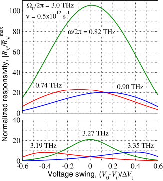
Figure 4 shows the dependences of the normalized responsivity, on the voltage swing calculated using equation (26) for different signal frequencies in the vicinity of the zeroth and first plasma resonances. The plasma frequency at was chosen to be THz . The plasma frequency at different values of is given by , where . At , nm, and cm-2, mV. We set and s-1. As seen from figure 4, an increase in the absolute value of the voltage swing results in a marked drop of the responsivity. It is also seen that detuning of the plasma resonance leads to a significant decrease in the responsivity (compare the curves for the plasma resonances at THz and THz with those corresponding to a detuning THz. Slightly different maximum values of the responsivity shifted from the plasma resonances are due to a small asymmetry of the resonant peaks. Different positions of these maxima are associated with the dependence of the plasma frequency on .
The excitation of plasma oscillation by electromagnetic signals can be used not only for the resonant reinforcement of the rectified current (i.e., the detector responsivity), but also for a more effective generation of higher harmonics 8 .
V Conclusions
In summary, we considered the dynamic behavior of the double-GL RT structures. We calculated the frequency-dependent admittance and the responsivity of the double-GL RT structures to the incoming signals as functions of the structural parameters, bias voltages, and frequency. It was demonstrated that the stationary states of the electron-hole plasma are stable with respect to the self-excitation of plasma oscillations and aperiodic perturbations for the structures with realistic parameters. As shown, the responsivity exhibits sharp resonant maxima corresponding to the excitation of plasma modes by incoming electromagnetic radiation. The plasma oscillations and the pertinent responsivity peaks are in the THz range. The responsivity of the double-GL RT detectors operating at room temperature can exhibit very high values markedly exceeding V/W.
Acknowledgments
The work was supported by the Japan Science and Technology Agency and the Japan Society for Promotion of Science, PIRE TeraNano Program, NSF, USA, and the Army Research Laboratory under ARL MSME Alliance, USA.
References
- (1) Liu M, Yin X, Ulin-Avila E, Geng B, Zentgraf T, Ju L, Wang F and Zhang X 2011 Nature 474 64
- (2) Britnell L, Gorbachev R V, Jalil R, Belle B D, Shedin F, Mishenko A, Georgiou T, Katsnelson M I, Eaves L, Morozov S V, Pres N M R, Leist J, Geim A K, Novoselov K S, and Ponomarenko L A 2012 Science 335 947
- (3) Liu M, Yin X and Zhang X 2012 Nano Lett. 12 1482
- (4) Georgiou T, Jalil R, Bellee B D, Britnell L, Gorbachev R V, Morozov S V, Kim X-J, Cholinia A, Haigh S J, Makarovsky O, Eaves L, Ponimarenko L A, Geim A K, Nonoselov K S and Mishchenko A 2013 Nature Nanotechnology 8 100
- (5) Ryzhii V, Otsuji T, Ryzhii M and Shur M S 2012 J. Phys. D 45 302001.
- (6) Ryzhii V, Ryzhii M, Mitin V, Shur M S, Satou A, and Otsuji T 2013 J. Appl. Phys. 113…
- (7) Feenstra R M, Jena D, and Gu G 2012 J. Appl. Phys 111 043711
- (8) Zhao P, Feenstra R M, Gu G, Jena D 2013 IEEE Trans. Electron Devices 60 951
- (9) Vasko F T 2013 Phys. Rev.B 87 075424
- (10) Britnel L, Gorbachev R V, Geim A K, Ponomarenko L A, Mishchenko A, Greenaway M T, Fromhold T M, Novoselov K S and Eaves L 2013 Nature Comm. 4 1794
- (11) Luryi S 1988 Appl. Phys. Lett. 52 501
- (12) Svintsov D , Vyurkov V, Yurchenko S, Otsuji T, and Ryzhii V 2012 J. Appl. Phys. 111 083715
- (13) Shur M 1990 Physics of Semiconductor Devices (Englewood Cliffs, NJ: Prentice-Hall)
- (14) Ryzhii V, Satou A and Otsuji T 2007 J. Appl. Phys. 101 024509
- (15) Rudin S 2011 Int. J. High Speed Electronics and Systems 20 567
- (16) Stauber T and Gomez-Santos G 2012 Phys. Rev. B 85 075410
- (17) Zhu J -J, Badalyan S M and Peters F M 2013 Phys. Rev. B 87 085401
- (18) Ryzhii V 2006 Jpn. J. Appl. Phys. 45 L923
- (19) Ryzhii V and Shur M 2001 Jpn J. Appl. Phys. 40 546
- (20) Kanaya H, Shibayama H, Sogabe R, Suzuki S and Asada M 2012 Appl. Phys. Express 5 124101