Photon-induced thermal effects in superconducting coplanar waveguide resonators
Abstract
We experimentally investigated the optical responses of a superconducting niobium resonator. It was found that, with increasing radiation power, the resonance frequency increases monotonically below around 500 mK, decreases monotonically above around 1 K and exhibits a nonmonotonic behavior at around mK. These observations show that one can operate the irradiated resonator in three temperature regimes, depending on whether two-level system (TLS) effects or kinetic inductance effects dominate. Furthermore, we found that the optical responses at ultra-low temperatures can be qualitatively regarded as a photon-induced thermalization effect of TLSs, which could be utilized to achieve thermal sensitive photon detections.
In recent years superconducting coplanar waveguide (CPW) resonators have attracted extensive attentions, due to its important applications in solid-state quantum information processings and sensitive photon detections pkday1 ; gao1 ; Baselmans1 ; Mazin1 . Particularly, high-quality factor resonators Barends1 ; Vissers1 ; Megrant1 (typically ) operating well below transition temperature have been demonstrated to be suitable for serving as so-called microwave kinetic inductance detectors (MKIDs) Zmuidzinas . According to Mattis-Bardeen theory Zmuidzinas2 , the absorption of photons (or increasing bath temperature) will decrease the electron-pair density in superconducting film, causing an increase in the kinetic inductance Mazin2 and thus a decrease in the resonance frequency. Meanwhile, the dissipation increases due to quasiparticle excitations, leading to a reduction in the quality factor. Therefore by probing the changes in the frequency or dissipation of a MKID, the radiation light signals can be detected. Much work to date have been done to optimize resonator geometries and materials as well as a better understanding of the noise properties in order to improve the detection sensitivity of MKID gao2 ; Barends2 ; Leduc .
In this paper we try to demonstrate another possible photon detection approach with a superconducting resonator. This approach is based on the thermalization of two-level systems (TLSs) in dielectrics rather than the kinetic inductance effects in the metal film. With a high-quality factor niobium resonator, we studied its optical responses by performing transmission measurements at low temperatures in a broad range of mK to K, well below the niobium transition temperature K. We found that the irradiated niobium resonator can be operated in three temperature regimes: with increasing radiation power, the resonance frequency increases monotonically below mK, decreases monotonically above K and exhibits an interesting nonmonotonicity at temperatures around mK. Similar crossover behavior with bath temperature for a unirradiated resonator have been reported gao3 ; Barends3 ; gao4 ; Lindstrom ; gao5 . Our observations can be qualitatively explained by the temperature dependent permittivity (due to TLSs in dielectrics) and temperature dependent kinetic inductance. At sufficiently low temperatures, TLS effects dominate over kinetic inductance effects, suggesting that the photon-induced thermalization effects of TLSs in dielectrics could be utilized to achieve thermal sensitive photon detections. Note that this is a different photon detection approach from MKID, which typically requires a superconducting material and geometry with high kinetic inductance fraction Porch .
Our CPW resonator Wang was fabricated by magnetron sputtering and photolithography. A nm thick niobium film was deposited on a m thick high-resistivity silicon substrate. Contact exposure as well as reflect ion etching were used to generate desired patterns on the film. The microscope photograph of the key structure of the measured sample is shown in Fig. 1(a). The resonator is actually a meandered transmission line, which shorts to the ground plane at one end and capacitively couples to a feedline at another end. The feedline is m wide with a gap of m to the ground plane. The center line of the resonator is m wide with a gap of m. The total length of the resonator is about mm and the relative permittivity of Si substrate is , giving a theoretical fundamental resonance frequency GHz.
The resonator chip is glued and wire-bonded to a gold-plated oxygen-free copper box equipped with microwave connections. This sample box is mounted at the cold plate of the mixing chamber in a dilution refrigerator with base temperature less than mK. The temperature was measured using a calibrated R1101 resistance thermometer which is placed close to the sample box. To radiate the CPW resonator, a single-mode optical fiber is set up from the room temperature down to the sample box. A room temperature laser source is connected to the top end of the fiber and generates a steady stream of photons at wavelength nm. The bottom end of the fiber is carefully aligned and fixed so that the incoming photons can hit the short end area of the resonator, where the standing wave current distribution is maximum. The fiber end is about m vertically away from the chip surface and the irradiation area (indicated by the red circle in Fig. 1(b)) is about m in diameter. Therefore, part of the incoming photons are incident on the superconducting film and part on the bare substrate in the gap. Additionally, not all the photons are absorbed by the chip, as some photons could be reflected and scattered into the environment.
The device transmission amplitudes as a function of frequency were measured with an Agilent E5071C vector network analyzer. Attenuators and DC blocks are positioned appropriately to suppress circuit noises. The microwave driving power reaching the chip is estimated to be about dBm, which is fixed for all the measurements in this letter. At temperature mK, a resonance dip was found at GHz, shown in Fig. 1(c). Note that the resonance curves have been calibrated to measure dB off resonance to remove the effects of attenuation in the circuits. By fitting the data to a skewed Lorentzian model Gao-phd , one can obtain the loaded quality factor of the resonator = . We then radiated the resonator with a power nW and measured the transmissions when the system reaches thermal and electric equilibrium. As shown in Fig. 1(c), the resonance frequency shifts to a higher value GHz and the quality factor decreases to = . The decrease in quality factor is expected but the increase in resonance frequency is in contrary to the prediction of Mattis-Bardeen theory.
We now investigate the optical responses of the resonator with different radiation powers. To this aim we varied the light intensity and measured corresponding microwave transmissions through the resonator at base temperature = mK. Fig. 2 (blue circles) shows the relative resonance frequency shift as a function of the radiation power on the short end area. Here, the relative frequency shift is defined as , with being the total radiation power entering the sample box and the corresponding resonance frequency. It is shown that the frequency shift increases monotonically with increasing radiation power in the range of nW to W. The inset shows the same plot except the power-axis is in logarithmic scale. One can see that the frequency shift increases approximately linearly with logarithmic power above a crossover point (at nW), indicated by the intersection of two red dotted lines.
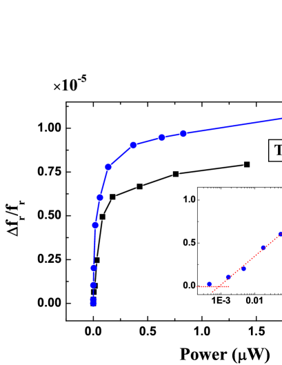
Qualitatively, the radiation power dependence observed here is similar to the temperature dependence reported in a few recent experiments gao3 ; Barends3 ; gao4 ; Lindstrom ; gao5 , where the measured resonance frequency shift shows approximately a logarithmic increase with temperature well below . Such behaviors were also verified in our measurements of the relative frequency shift versus bath temperature, as shown in Fig. 3.
Here, with the reference temperature mK. Note that the experiments can not be explained by Mattis-Bardeen theory, which predicts a frequency shift opposite in sign. Instead, the observed temperature dependence can be attributed to the TLS effects in dielectrics Martinis2 ; Martinis3 . In fact, TLSs are abundant in amorphous materials and can be present in substrate, the surface oxides on the metal film and the interface between metal and substrate Martinis . At low temperatures, the unsaturated TLSs with electric dipole moments can interact resonantly with the microwave field, giving a temperature dependent variation of permittivity Phillips . Changing in permittivity affects the capacitance per unit length and thus the resonance frequency. Assuming a uniform distribution of TLSs, the relative resonance frequency shift is given by gao3
| (1) |
where is the unique fitting parameter, mK the reference temperature and with being the complex digamma function. Fits to the above equation ( ) can explain the observed temperature dependence below K, where the resonance frequency increases monotonically with temperature. This suggests that at low temperatures , which is the case here, the thermal effects on the kinetic inductance are relatively weak Meservey . Additionally, considering the geometry of our resonator, its kinetic inductance fraction is estimated to be very small (less than ). Therefore the kinetic inductance effects are negligible for and TLS effects become prominent, which is the reason why Mattis-Bardeen theory does not describe the dominating loss mechanism at ultra-low temperatures. However, the resonance frequency starts to drop at around K, indicating that TLS effects saturate and kinetic inductance becomes dominant as temperature approaching . Similar experimental results have been observed in a NbTiN resonator covered with SiOx layer Barends3 .
We believe that the above TLS effects can also explain the observed radiation power dependence at mK. Experimentally, photons irradiated on both metal film and substrate will mainly heat the chip and increase its effective temperature, although the bath temperature does not change. At ultra-low temperatures(e.g., mK), the incident photons can excite TLSs in the substrate, especially those in the exposed substrate surface (i.e., SiOx in our device) and nearby the irradiated area. To further verify it is indeed the thermalization of TLSs in the substrate dominates the radiation power dependence of resonance frequency at ultra-low temperatures, we also directly radiated on a small area of the bare substrate, which is about mm away from the resonator. We performed the relevant transmission measurements at mK and obtained a similar radiation power dependence, as shown in Fig. 2 (black squares). The similar power dependence implies that the thermalization of TLSs is the main factor in shifting the resonace frequency. Moreover, the photon responsivity is weaker when radiating on the bare substrate of a certain distance away from the resonator than that when radiating on the short end area. This is reasonable and can be explained by a nonuniform temperature distribution around the irradiated area. The effective temperature at the RF active component of the resonator is lower when the m thermal source is moved mm away.
We then investigated the optical responses of the resonator at different bath temperatures. Fig. 4(a) shows the relative resonance frequency shift as a function of radiation power, taken at seven selective bath temperatures in a broad range of mK - mK. Here, the relative frequency shift is defined as , with being the bath temperature and the radiation power. Note that the reference frequency varies with temperature . At lower temperatures (i.e., mK, mK, mK and mK), the frequency shift increases monotonically with increasing radiation power, indicating the TLS effects dominate in this temperature range. Apparently, the resonator responsivity to photons is strongest at the lowest temperature mK. For the temperature at mK, we observed an interesting phenomenon that the resonance frequency exhibits a nonmonotonic behavior with increasing radiation power: the frequency firstly goes down and then goes up, which can be seen more clearly in Fig. 4(b). This suggests that the kinetic inductance effects start to play in role at the temperature around mK and the TLS effects are less pronounced than those at ultra-low temperatures. With lower radiation power, the incident photons break Cooper pairs near the irradiated area, increasing the kinetic inductance and decreasing the resonance frequency. However, with enhancing radiation power, the chip is heated to excite the unsaturated TLSs and the TLS effects may become dominated over the kinetic inductance effects again, causing the resonance frequency increase. Furthermore, for higher temperatures, e.g. at mK and mK, the frequency decreases monotonically with radiation power. As temperatures increase, the TLS effects tend to fully saturate. Therefore only kinetic inductance changes with incident photons in high temperature regime.
In summary, we experimentally studied the optical responses of a superconducting niobium coplanar waveguide resonator at various temperatures. Our results show that one can operate an irradiated Nb resonator in three different temperature regimes below . At ultra-low temperatures (below mK), TLS effects dominate while at higher temperatures (above K), TLS effects saturate and kinetic inductance effects dominate. In the middle regime (e.g., around mK), both TLSs and kinetic inductance take effects. Therefore, instead of maximizing the kinetic inductance effects to improve the performance of MKID for sensitive photon detections, the TLS effects could also be utilized to achieve weak light detections at ultra-low temperatures. Furthermore, lower bath temperatures lead to stronger photon responses.
Although the sensitivity of the TLS-based photon detections demonstrated here is much lower than that of a MKID, the relevant resonator is relatively easy to be fabricated since high kinetic inductance fraction is not required. The performance of proposed TLS-based weak light detections could be improved by minimizing the heat capacity of the chip. The chip size can be designed and fabricated as small as possible so that a certain radiation power can lead to a bigger effective temperature change of the resonator. Also, an antireflection-coating can be used to reduce photon reflections and achieve a high optical coupling efficiency. In addition, increasing the density of TLSs in dielectrics will enhance the TLS-resonator coupling and thus in principle may improve the device sensitivity to incident photons.
This work was supported in part by the National Natural Science Foundation (Grant No. 61301031, No. 11174373, No. 11204249), and the National Fundamental Research Program of China (Grant No. 2010CB923104). We thank Profs. Y. Yu and P. H. Wu for kind supports and discussions.
References
- (1) P. K. Day, H. G. LeDuc, B. A. Mazin, A. Vayonakis, and J. Zmuidzinas, Nature(London) 425, 817 (2003).
- (2) J. Gao, M. R. Visser, M. O. Sandberg, F. C. S. da Silva, S. W. Nam, D. P. Pappas, D. S. Wisbey, E. C. Langman, S. R. Meeker, B. A. Mazin, H. G. Leduc, J. Zmuidzinas, and K. D. Irwin, Appl. Phys. Lett. 101, 142602 (2012).
- (3) J. Baselmans, S. Yates, P. Diener, and P. Visser, J. Low Temp. Phys. 167, 360 (2012).
- (4) B. A. Mazin, B. Bumble, S. R. Meeker, K. Brien, S. McHugh, and E. Langman, Optics Express 20(2), 1503 (2012).
- (5) R. Barends, N. Vercruyssen, A. Endo, P. J. de Visser, T. Zijlstra, T. M. Klapwijk, P. Diener, S. J. C. Yates, and J. J. A. Baselmans, Appl. Phys. Lett. 97, 023508 (2010).
- (6) M. R. Vissers, J. Gao, D. S. Wisbey, D. A. Hite, C. C. Tsuei, A. D. Corcoles, M. Steffen, and D. P. Pappas, Appl. Phys. Lett. 97, 232509 (2010).
- (7) A. Megrant, C. Neill, R. Barends, B. Chiaro, Yu Chen, L. Feigl, J. Kelly, Erik Lucero, Matteo Mariantoni, P. J. J. Malley, D. Sank, A. Vainsencher, J. Wenner, T. C. White, Y. Yin, J. Zhao, C. J. Palmstrom, John M. Martinis, and A. N. Cleland, Appl. Phys. Lett. 100, 113510 (2012).
- (8) J. Zmuidzinas, Annu. Rev. Cond. Mater. Phys. 3, 169 (2012).
- (9) J. Gao, J. Zmuidzinas, A. Vayonakis, P. Day, B. Mazin, and H. Leduc, J. Low Temp. Phys. 151, 157 (2008).
- (10) B. A. Mazin, Microwave kinetic inductance detectors, Ph.D. thesis (California Institute of Technology, 2004).
- (11) J. Gao, J. Zmuidzinas, B. A. Mazin, Henry G. LeDuc, and Peter K. Day, Appl. Phys. Lett. 90, 102507 (2007).
- (12) R. Barends, N. Vercruyssen, A. Endo, P. J. de Visser, T. Zijlstra, T. M. Klapwijk, and J. J. A. Baselmans, Appl. Phys. Lett. 97, 033507 (2010).
- (13) H. Leduc, B. Bumble,P. Day, B. Eom, J. Gao, S, Golwala, B. Mazin, S. McHugh, A. Merrill, D. Moore, O. Noroozian, A. Turner, and J. Zmuidzinas, Appl. Phys. Lett. 97, 102509 (2010).
- (14) J. Gao, M. Daal, A. Vayonakis,S. Kumar, J. Zmuidzinas, B. Sadoulet, B. A. Mazin, P. K. Day, and H. G. Leduc, Appl. Phys. Lett. 92, 152505 (2008).
- (15) R. Barends, H. L. Hortensius, T. Zijlstra, J. J. A. Baselmans, S. J. C. Yates, J. R. Gao, and T. M. Klapwijk, Appl. Phys. Lett. 92, 223502 (2008).
- (16) S. Kumar, J. Gao, J. Zmuidzinas, B. A. Mazin, H. G. LeDuc, and P. K. Day, Appl. Phys. Lett. 92, 123503 (2008).
- (17) T. Lindstrom, J. E. Healey, M. S. Colclough, C. M. Muirhead, and A. Ya. Tzalenchuk, Phys. Rev. B 80, 132501 (2009).
- (18) D. S. Wisbey, J. Gao, M. R. Vissers, F. C. S. da Silva, J. S. Kline, L. Vale, and D. P. Pappas, J. Appl. Phys. 108(9), 093918 (2010).
- (19) A. Porch, P. Mauskopf, S. Doyle, and C. Duscombe, IEEE Trans. Appl. Superconduct. 80, 552 (2005).
- (20) H. Li, Y. Wang, L. Wei, P. Zhou, Q. Wei, C. Cao, Y. Fang, Y. Yang, and P. Wu, Chin. Sci. Bull. 58(20), 2413 (2013).
- (21) J. Gao, Ph. D. thesis, Caltech, 2008.
- (22) John M. Martinis, K. B. Cooper, R. McDermott, Matthias Steffen, Markus Ansmann, K. D. Osborn, K. Cicak, Seongshik Oh, D. P. Pappas, R. W. Simmonds, and Clare C. Yu, Phys. Rev. Lett. 95, 210503 (2005).
- (23) R. W. Simmonds, K. M. Lang, D. A. Hite, S. Nam, D. P. Pappas, and John M. Martinis, Phys. Rev. Lett. 93, 077003 (2004).
- (24) J. Wenner, R. Barends, R. Bialczak, Y. Chen, J. Kelly, E. Lucero, M. Mariantoni, A. Megrant, P. Malley, D. Sank, A. Vainsencher, H. Wang, T. White, Y. Yin, J. Zhao, A. Cleland, and J. M. Martinis, Appl. Phys. Lett. 99, 113513 (2011).
- (25) W. A. Phillips, Rep. Prog. Phys. 50, 1657 (1987)
- (26) R. Meservey and P. M. Tedrow, J. Appl. Phys. 40, 2028 (1969)