Radius-Voltage Relation of Graphene Bubbles Controlled by Gate Voltage
Abstract
Graphene on the substrate can form bubbles rising above the sheet. In some cases, the bubble is a perfect spherical surface crown, and its radius can be adjusted by external electric field. In this manuscript, we theoretically investigate the voltage dependence of the spherical bubble’s radius. The calculated results are in good agreement with recent experiments on the graphene bubble controlled by applied gate voltage [Appl. Phys. Lett. 99, 093103 (2011)].
pacs:
61.48.-c, 61.48.Gh, 62.25.-gGraphene, the two-dimensional honeycomb structure consisting of a single atomic layer of carbon, is the subject of intensive studies due to its distinctive electronic mobility geim07 ; geim09 , high thermal conductivity balandin08 ; wang11 and high mechanical strength frankand07 ; cranford11 ; mu09 . With its extraordinary properties, graphene has many electronic lin10 ; mu11 , mechanical bunch07 , photonic li09 ; xia09 , thermal yang09 ; hu09 ; zhang11 , chemical ling10 , and acoustic applications tian11 . Moreover, graphene is an extremely interesting candidate for micro- and nanoelectromechanical systems (MEMS/NEMS). MEMS/NEMS are devices integrating electrical and mechanical functionality on the same devices. In the design of NEMS devices, the coupling between electrical and mechanical performance is very important. One recent experiment georgiou11 found that spherical graphene bubbles can be stable in large size on top of silicon oxide substrate with the bubble radius of graphene spherical bubbles can be controlled by the gate voltage. This may open up graphene’s application as optical lenses with adjustable focal length. However, there still lacks an analytical expression of the gate voltage dependence of the bubble radius in the literatures. In the present work, we will fulfill this task.
Among the efforts on the studies of the bubbles rising in graphene sheet bunch08 ; levy10 ; zong10 ; koenig11 ; zabel12 ; yue2012 , Yue et al. yue2012 proposed a method to theoretically reproduce the shape of a stable graphene bubble observed by Georgiou et al.. The equilibrium shape of the bubble is determined by finding the minimum of the free energy containing elastic, adhesion and pressure terms, , where is the pressure of air molecules ”sealed” inside the bubble, and is the pressure outside the bubble. We extend this model to describe electromechanical coupling by including the capacitive energy for electrostatic interaction. The main idea of the present work is to introduce a gate voltage dependent correction for adhesion energy term, , with being the Metal-Oxide-Semiconductor (MOS) capacitance per unit area for the graphene/SiO2/Si structure in Georgiou et al.’s experiment, as shown in Fig.1(a). The expansion and shrinkage of a bubble change the area of the substrate covered by the graphene sheet, thus changing the stored electrostatic energy (capacitive energy) in this MOS system. On the other side, a spherical graphene bubble will expand (shrink) to one with larger (smaller) and , (see Fig.1(b)) in response to the decreasing (increasing) of gate voltage.
In present work, graphene is modeled as a flexible membrane with only one layer of carbon atoms. The elastic energy can be described by yakobson96
| (1) |
Here, the first term on the right hand side of Eq. (1) is the strain energy, and the second term is the curvature energy. The and are local curvatures, , are the D Young’s modulus and D bending modulus, respectively, with is the thickness of a mono-layer graphene. The Possion’s ratio is reported around yue2012 . The integral is over the whole area of the spherical graphene bubble.
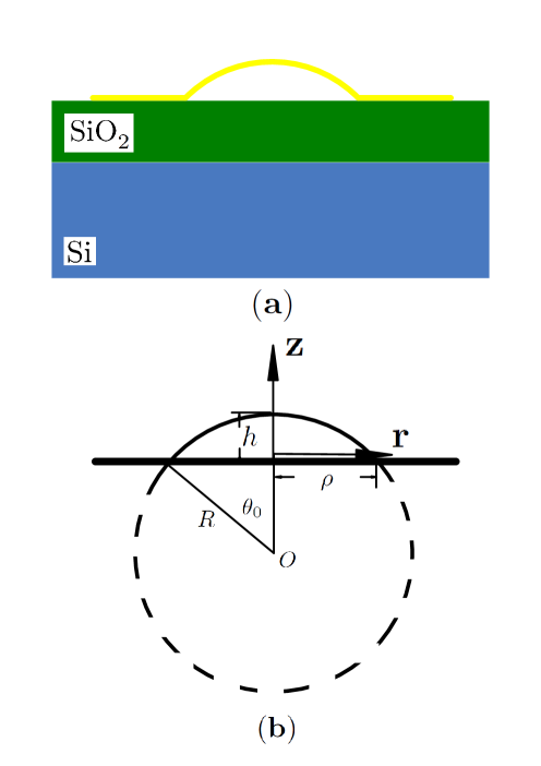
As an initial estimation, the average strain in a spherical bubble of graphene is about , and (the definition of is shown in Fig. 1,zong10 while the curvatures are and , the elastic energy with this isotropic strain energy has a form of
| (2) |
thus the ratio of the two types of elastic energy is , with . Since , , and , georgiou11 , only strain energy matters for graphene bubble observed in Ref. georgiou11, . The total strain energy is estimated to be approximately , for .
A more accurate description of the elastic energy of the stretched carbon membrane with a bubble needs the knowledge of the strain distribution on the curved bubble surface. The axis-symmetric deflection profile of bubble was suggested to be approximately yue2012
| (3) |
with the height of the spherical crown and the radius of the circular area of substrate without the coverage of graphene sheet. Equation (3) is reasonable due to the fact that typically . The axis-symmetric distribution of radical displacement of the bubble is proposed as,
| (4) |
This strain distribution ensures that and reaches its maximum at . The elastic energy can be expressed by the radial and circumferential strains yue2012 ,
| (5) |
Here, the radial strain is , and the circumferential strain is .
Usually, separating a monolayer graphene adhering on the top of the silicon dioxide substrate costs adhesion energy per unit area . koenig11 However, in the Georgiou et al.’s experiment, the graphene layer can not stick to the rough substrate tightly, and there is also hydrophobic interaction caused by the present of water molecules in the gap between the graphene and rough substrate, which dramatically lowers the measured adhesion energy per unit area to .
The total potential energy for the graphene bubble has a form,
| (6) |
With fixed radius , the equilibrium condition leads the potential energy yue2012
| (7) |
Here, is the number of air molecules trapped in the bubble, which is constant due to the impermeability of graphene.bunch08 The first term in the right hand side of Eq. (7) is the strain energy stored in graphene, which is independent of the bubble geometry. The second term is the potential energy of the air molecules. As increases, the total potential energy decreases, while the adhesion energy increases due to part of the graphene is detached from the substrate. The equilibrium condition,
| (8) |
gives rise to the the adhesion energy per unit area yue2012
| (9) |
As we have emphasized, the MOS capacitance plays the key role in the electromechanical coupling of the graphene bubble. The simplest way to describe MOS capacitance is the parallel plate capacitor approximation, , with the thickness of the oxide layer. The gate voltage dependent radius of the graphene spherical bubble is obtained as,
| (10) |
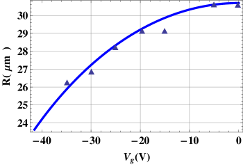
Yue et al. yue2012 found that with the gate voltage changing from to , only varies a little around in Georgiou et al.’s experiment. The , which is of the ”contact angle” of the bubble, varies little too. In Table 1, we list the for a set of negative gate voltages extracted from Ref. georgiou11, .
| (V) | -35 | -25 | -15 | 0 |
|---|---|---|---|---|
| 0.072 | 0.068 | 0.066 | 0.065 |
Equation (10) has a form . This relation are in good agreement with Georgiou et al.’s experiment, georgiou11 as shown in Fig. 2. The fitted adhesion energy is , which is in accordance with the result in Ref. yue2012, . The theoretical calculated thickness of the silicon dioxide is about , which is also comparable to the experimental measurement of thickness. georgiou_new Therefore, our simple model captures the basic physics of the electromechanical coupling in the gate voltage controlled graphene bubble rising on the substrate.
In summary, we have theoretically investigated the gate voltage dependence of radius of the graphene spherical bubble observed by Georgiou et al. Base on the elastic membrane theory, we find this phenomenon is governed by the gate voltage dependent adhesion energy. In Georgiou et al.’s experiment, the adhesion energy is sufficiently lowered by the water molecules trapped between the graphene and substrate. The key point of the gate voltage controlled expansion/ shrinkage of the graphene bubble is the adhesion energy modified by capacitive energy, which affects the mechanical balance of the equilibrium shape of the bubble. Present results can be used to find the design rules for the devices based on gate voltage controlled graphene bubble.
We gratefully acknowledge National Science Foundation of China (NSFC) under Grants No. 11074259, and the Major Research Plan of the National Natural Science Foundation of China (Grant No. 91027045) for the support of this work. We are grateful to Dr. Linying Cui for her modifying this manuscript.
References
- (1) A. K. Geim, and K. S. Novoselov, Nat. Mater. 6, 183 (2007).
- (2) A. K. Geim, Science, 324, 1530 (2009).
- (3) A. A. Balandin, S. Ghosh, W. Bao, I. Calizo, D. Teweldebrhan, F. Miao, and C. N. Lau, Nano Lett. 8, 902 (2008).
- (4) Z. Wang, R. Xie, C. T. Bui, D. Liu, X. Ni, B. Li and J. T. L. Thong, Nano Lett. 11, 113 (2011).
- (5) I. W. Frank, D. M. Tanenbaum, A. M. van der Zande, and P. L. McEuen, and J. Vac. Sci. Technol. B 25, 2558 (2007).
- (6) S. W. Cranford, and M. J. Buehler, Carbon, 49, 4111 (2011).
- (7) W. Mu, M. Li, W. Wang, and Z-c. Ou-Yang, New J. Phys. 11, 113049 (2009).
- (8) Y. M. Lin, C. Dimitrakopoulos, K. A. Jenkins, D. B. Farmer, H. Y. Chiu, A. Grill, and P. Avouris, Science, 327, 662 (2010).
- (9) W. Mu, G. Zhang, Y. Tang, W. Wang, and Z-c. Ou-Yang, J. Phys: Condens. Matter, 23 495302 (2011).
- (10) J. S. Bunch, A. M. van der Zande, S. S. Verbridge; I. W. Frank, D. M. Tanenbaum, J. M. Parpia, H. G. Craighead, and P. L. McEuen, Science, 315, 490 (2007).
- (11) X. S. Li, Y. W. Zhu, W. W. Cai, M. Borysiak, B. Y. Han, D. Chen, R. D. Piner, L. Colombo, and R. S. Ruoff, Nano Lett. 9, 4359 (2009).
- (12) F. N. Xia, T. Mueller, Y. M. Lin, A. V. Garcia, and P. Avouris, Nat. Nanotechnol. 4, 839 (2009).
- (13) N. Yang, G. Zhang and B. Li, Appl. Phys. Lett. 95, 033107 (2009).
- (14) J. Hu, X. Ruan and Y. P. Chen, Nano Lett. 9, 2730 (2009).
- (15) G. Zhang and H. S. Zhang, Nanoscale, 3, 4604 (2011).
- (16) X. Ling, L. Xie, Y. Fang, H. Xu, H. Zhang, J. Kong, M. S. Dresselhaus, J. Zhang, and Z. Liu, Nano Lett. 10 553 (2010)
- (17) H. Tian, T-L. Ren, D. Xie, Y-F. Wang, C-J. Zhou, T-T. Feng, D. Fu, Y. Yang, P-G. Peng, L-G. Wang, and L-T. Liu, ACS Nano. 5, 4878 (2011).
- (18) T. Georgiou, L. Britnell, P. Blake, R. V. Gorbachev, A. Gholinia, A. K. Geim, C. Casiraghi, and K. S. Novoselov, Appl. Phys. Lett. 99, 093103 (2011).
- (19) J. S. Bunch , S. S. Verbridge , J. S. Alden , A. M. van der Zande , J. M. Parpia , H. G. Craighead and P. L. McEuen, Nano Lett. 8, 2458 (2008).
- (20) N. Levy, S. A. Burke, K. L. Meaker, M. Panlasigui, A. Zettl, F. Guinea, A. H. Castro Neto, and M. F. Crommie, Science 329, 544 (2010).
- (21) Z. Zong, C.-L. Chen, M. R. Dokmeci, and K.-T. Wan, J. Appl. Phys. 107, 026104 (2010).
- (22) S. P. Koenig, N. G. Boddeti, M. L. Dunn, and J. S. Bunch, Nat. Nanotechnol. 6, 543 (2011).
- (23) J. Zabel, R. R. Nair, A. Ott, T. Georgiou, A. K. Geim, K. S. Novoselov, and C. Casiraghi, Nano Lett. 12, 617 (2012).
- (24) K. Yue, W. Gao, R. Huang, and K. M. Liechti, J. Appl. Phys. 112, 083512 (2012).
- (25) B. I. Yakobson, C. J. Brabec, and J. Bernholc, Phys. Rev. Lett. 76, 2511 (1996).
- (26) T. Georgiou, private communication.