Resonant electron tunneling in a tip-controlled potential landscape
Abstract
By placing the biased tip of an atomic force microscope at a specific position above a semiconductor surface we can locally shape the potential landscape. Inducing a local repulsive potential in a two dimensional electron gas near a quantum point contact one obtains a potential minimum which exhibits a remarkable behavior in transport experiments at high magnetic fields and low temperatures. In such an experiment we observe distinct and reproducible oscillations in the measured conductance as a function of magnetic field, voltages and tip position. They follow a systematic behavior consistent with a resonant tunneling mechanism. From the periodicity in magnetic field we can find the characteristic width of this minimum to be of the order of 100 nm. Surprisingly, this value remains almost the same for different values of the bulk filling factors, although the tip position has to be adjusted by distances of the order of one micron.
I Introduction
Charging effects in the integer and fractional quantum Hall regime prove to be powerful tools to probe the properties of the respective particles. These effects offer for example the possibility to measure the charge of the particles Kou et al. (2012); McClure et al. (2012); Willett et al. (2009). Furthermore they are discussed as an option to prove possible non-abelian statistics of the 5/2-quasiparticle with a charge of 1/4 Nayak et al. (2008) which would make them a strong candidate to realize topological quantum computation. Fundamental aspects make the underlying physics very rich. It has been shown that many other properties can be efficiently explored by operating electron interferometers and quantum dots in the quantum Hall regime, e.g. to demonstrate the importance of interactions Rosenow and Halperin (2007); Ihnatsenka et al. (2009); Ofek et al. (2010) or to estimate the velocity and dephasing rate inside a quantum Hall edge channel McClure et al. (2009). Charging effects manifest themselves in an oscillatory pattern in the dependence of the conductance on both the magnetic field and a gate-voltage which influences the size of the confined geometry Kou et al. (2012); Ofek et al. (2010); Halperin et al. (2011); Zhang et al. (2009). Oscillations in rather small structures are usually dominated by a Coulomb charging- or resonant tunneling mechanism, while large interferometers can be understood based on an Aharanov-Bohm mechanism Kataoka et al. (1998); Zhang et al. (2009); Halperin et al. (2011).
Several different options exist to confine the current carrying particles in such a way that the above mentioned phenomena can be observed. The crucial point in all these experiments is an isolated island of compressible electron liquid, created in a two dimensional electron gas (2DEG) in a magnetic field. This can be done either by forming a quantum dot or an anti-dot Zhang et al. (2009); Kou et al. (2012). The experimental observations are similar in both cases. All experiments reported up to now used lithographic gates to confine the electron paths into certain geometries. The parameter space is thus spanned basically by the voltages which are applied to the gates, the source-drain bias voltage and the magnetic field. Previous scanning probe experiments used predefined structures and tried to explore the underlying physics with real space resolution Martins et al. (2013). In our experiments we define the potential landscape with the help of a quantum point contact (QPC) in combination with the biased tip of an atomic force microscope, offering an additional parameter directly influencing the geometry and thus obtaining an additional degree of freedom to tune the structure.
II Sample and experimental setup
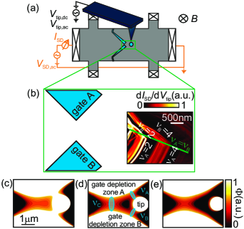
The experimental setup is schematically depicted in Fig. 1(a). We use a GaAs-AlGaAs heterostructure wafer hosting a 2DEG with an electron density of cm-2 and a mobility of cm2/Vs. The 2DEG is placed 120 nm below the surface. Top gates to define a QPC were patterned using electron beam lithography on top of a wet-etched Hall bar structure. We apply an ac-source-drain voltage of 20 V symmetrically with respect to ground and measure the source-drain current at the same time. The gold-top gates have an opening angle of 90∘ and are spaced by 800 nm at the point of minimum distance (see Fig. 1(a)). We use the conducting tip of a home-built cryogenic scanning force microscope (AFM) operating in a dilution refrigerator at a base temperature of 40 mK to locally perturb electron transport. For this purpose the tip is scanned at a height of 90 nm above the sample surface and a negative dc-voltage V is applied unless stated otherwise. This leads to a disc-shaped region of total depletion in the electron gas underneath, with a radius of about 1.2 m Pascher et al. (2014). We apply a small ac-voltage with an amplitude of 50 mV to the tip, in order to measure the transconductance . In most of the existing literature charging effects are directly visible as oscillations in Zhang et al. (2009); Ofek et al. (2010). In our measurements the oscillations in are very subtle and superimposed on a strongly varying background. It is therefore necessary to measure in order to enhance their visibility. The electron temperature in the experiment is about 170 mK, and a magnetic field is applied perpendicular to the 2DEG.
III Creating the potential minimum
Figures 1(c), (d) and (e) show schematically the potential landscape which is induced by the gates and the tip. Figures 1(c) and (e) show the extreme cases, where the tip is so close to the QPC, that it totally blocks transport or the tip is so far away, that it has practically no influence on the recorded current. The most interesting case occurs at intermediate tip-positions shown in Fig. 1(d), where two QPCs A and B form between the tip and the two top gates A and B Pascher et al. (2014). We can assign a different filling factor to each QPC. We name the filling factor in the center of the lithographic QPC and the filling factors of the QPCs which are caused by the tip and . The measured current is
| (1) |
where
| (2) |
A special situation arises, when all three filling factors are the same. As shown in Fig. 1(d) a potential minimum between the gates and the tip forms, which leads to localized states. The local filling factor inside the potential minimum can be tuned in a parameter space spanned by the external magnetic field , the gate-voltage , the tip voltage , and the tip position.
IV Finding the right spot in parameter space
IV.1 The symmetry line
The correct position for the tip has to be found, where and the puddle will form. In a first step we aim at finding the line where . For that purpose a constant voltage is applied to the QPC-gates in order to define the QPC. A voltage of V was chosen, which is enough to deplete the 2DEG underneath Rössler et al. (2011) but keeps maximal. Figure 1(b) shows an area-scan which was taken at a magnetic field of 2 T (bulk filling factor ) at a position about 2 away from the QPC-gap with the -axis of the scan frame oriented parallel to the QPC gap. The colors encode the transconductance measured with respect to the tip-voltage. To clarify the experimental geometry, the scanning gate microscopy (SGM)-image is put into relation to the position of the lithographic gates in real space, as indicated by the green frame. In this constellation, this means that is maximal and according to Eq. (2) and dominate.
The current saturates at the bulk-value which is fixed to the bulk filling factor . In the -map shown in Fig. 1(b) plateaus in the conductance as a function of tip position show up as black stripes. Broad black stripes correspond to perfect transmission of even integer quantum Hall edge states according to Eq. (2). Thus we can assign specific filling factors to the black stripes as indicated in Fig. 1(b). The green line marks a line of symmetry where . This line is not perpendicular to the QPC-gap, either because the left and the right topgate have a slightly different lever arm, or because the local potential landscape is not perfectly symmetric due to irregularities in the lithographic top gates or local effects of impurities Rössler et al. (2011).
IV.2 Closing the quantum point contact
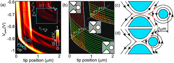
Now that the line where is found, we need to find the tip position where . The line is repeatedly scanned, while the voltage on the QPC-gates is changed after each line is finished. Exemplary results are presented in Fig. 2 for a magnetic field of 2 T corresponding to a bulk filling factor (Fig. 2(a)) together with schematics to explain the prominent features (Figs. 2(b) - (d)). Different bulk filling factors show qualitatively similar results.
In these line scan-images we can distinguish two different regimes, as illustrated in Fig. 2(b): At relatively low gates-voltages and small distance between QPC and tip (top left corner of Fig. 2(b)) and dominate, because . In this regime, the pattern does not depend on the gate-voltage, yet the tip position has a huge influence. This regime is marked by the red parallel lines in Fig. 2(b). At larger gate voltages and larger tip-QPC separation (bottom right corner of Fig. 2(b)) dominates, because , as illustrated by the green lines in Fig. 2(b). In this regime the dependence on the tip position is less pronounced than before. The shape of this curve as a function of position and voltage reflects the tip-induced potential.
In this parameter space we find lines where which form the boundaries between two cases (see Fig. 2(b)). This is where the above mentioned potential minimum between tip and QPC can be found. We find resonances at every transition between local filling factors (see blue frames in Fig. 2(a)). The transition between and is shown in Fig. 2(c): One spin degenerate edge channel is fully transmitted, one is reflected by the SGM-tip. At the transition between filling factors and the situation (see Fig. 2(d)) is similar, although the oscillation pattern is not clearly visible in Fig. 2(a).
V Parameter dependencies of oscillations
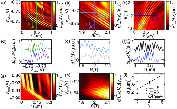
In order to characterize the parameter-dependencies of the observed oscillations quantitatively, we zoom into the regions within the blue frames in Fig. 2(a) at the bulk filling factor of 4. These correspond to the transition regions between filling factors 2 and 4 in the case of frame (c) and between 0 and 2 for the case of frame (d). In both cases the zooms reveal an oscillatory pattern, as shown in Figs. 3(a) and (g). At the transition between pinch off and the local filling factor 2 the signal is rather weak, which makes it necessary to plot the second derivative in order to achieve significant contrast.
V.1 Magnetic field dependence of oscillations
When the tip is placed at a fixed position, the dependence of the oscillations on , and can be measured. The resulting oscillation periods are named , and . The distance between tip and QPC-gap on the high symmetry line is and needs to be changed to adjust different filling factors. In Fig. 3(b) the dependence of the oscillatory pattern as a function of and is plotted. A stripe-pattern with a positive slope is observed. The periods and can be read from the linecuts, as shown in Figs. 3(d) - (f). Sweeping the voltage on the tip instead of the gates leads to qualitatively similar pictures (not shown). The same measurements (Figs. 3 (g), (h)) were performed at the position of the blue frame (d) in Fig. 2(a).
To illustrate the reproducibility of the measurement results, traces which were taken in different measurements as a function of the same parameter are compared in Figs. 3(d) - (f). The curves were vertically offset for clarity. Lines in Figs. 3(a) - (c) encode which traces are shown in (d) - (f). Matching colors were chosen. The positions of the peaks agree very well, their intensities are slightly different. These measurements were taken in the order of one day apart, which leads to these small changes in the sample which give rise to small differences.
| (mT) | (mV) | () | (nm) | |||
| 2 mT | 1 mV | 10 mV | 0.02 | 3 nm | ||
| 6 | 6 … 4 | 16 | 13 | 403 | 4.32 | 117 |
| 4 … 2 | 27 | 8 | 150 | 3.18 | 110 | |
| 2 … 0 | 59 | 5 | 48 | 2.43 | 106 | |
| 4 | 4 … 2 | 25 | 9 | 171 | 3.36 | 115 |
| 2 … 0 | 45 | 11 | 52 | 1.83 | 121 | |
| 2 | 2 … 0 | 41 | 8 | 149 | 3.41 | 127 |
V.2 Interpretation
In the existing literature several possible mechanisms are discussed to understand conductance oscillations in confined geometries in quantum Hall systems. The positive slope in the conductance maps as a function of the magnetic field and gate voltage observed in the present investigation shows, that an increase of the magnetic field needs to be compensated by an increased gate voltage, as it would be the case for a Coulomb charging mechanism Rosenow and Halperin (2007); Zhang et al. (2009). Fundamental to our analysis will be the assumption that within each oscillation period, one electron is added to the island.
At the position of the potential minimum there is one edge channel which circulates in a closed loop, as illustrated in Figs. 2(c) and (d). A change in magnetic field changes the energy of the Landau levels and their degeneracy. A change in magnetic field will change the number of electrons on the localized island, which means that
| (3) |
where A is the area of the island and is its filling factor. A change of the magnetic field by one flux quantum per area leads to additional electrons on the island. Whenever two consecutive occupation numbers are degenerate, Coulomb blockade of the island is lifted which gives rise to conductance oscillations with a period . Changing or leads to a similar effect on the number of electrons on the island. Electrons will tunnel to the transmitted edge channels and conductance oscillations will be observed.
Figure 3(c) shows the evolution of the oscillation pattern as a function of tip position along the line . Moving the tip has an effect on the area of the localized region, if the tip is moved further away from the QPC, the area should increase. Thus the first effect which influences the shape of the oscillation pattern is the non-linear tail of the Lorentzian potential, which is induced by the tip. The second effect describes the dependence on a change of the magnetic field Halperin et al. (2011); Baer et al. (2013). If is increased, the population of the highest Landau level is decreased. This reduced electron density in the edge channels leads to an increased oscillation period at higher magnetic fields.
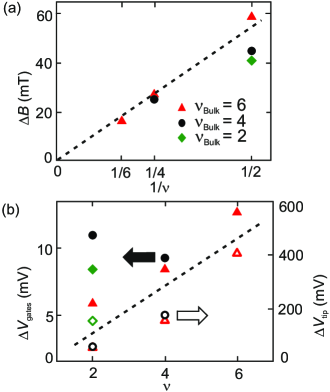
All oscillation periods which were extracted are summarized in Tab. 1. Similar measurements as presented in Fig. 3 for were also performed for and (not shown). The quoted errors are the standard deviations for period values which are extracted from traces like those shown in Fig. 3(d) – (f). A small systematic error is included, which is due to a linear increase of the peak spacing with higher gate- or tip-voltages. The error in describes the uncertainty in deducing the exact position of the QPC-gap during SGM-measurements. The periods as a function of 1/ show a linear behavior (see Fig. 4 (a)), consistent with Eq. (3). With the help of Eq. (3) we can estimate the size of the island from which is found to be always very similar (see Tab. 1). Assuming an approximately circular shape, we can calculate a radius =(12010) nm. With the help of a capacitor model we can estimate the charging energy of the island with this radius to be meV. As this energy is needed to change the charge on the island by one electron, the axes , and can be directly translated into energies via the peak spacings. From the full width at half maximum of the resonance peaks we can estimate the strength of the tunneling coupling . A Lorentzian fit to the peaks yields a value ) meV. Thus the system is in a regime, where the charge on the island is still approximately quantized, but the island is strongly coupled to the transmitting edge channels. No clear Coulomb blockade diamonds can be measured in this regime, as we verified experimentally.
In Fig. 4(b) we show the oscillation periods and as a function of filling factor. If the only effect of the tip or the gates is to change the electron number on the island, the periods and should be constant for all filling factors Zhang et al. (2009). In our case changing , or does not only change the electron number, but also the size of the island. Thus the periods and vary.
To adjust a particular filling factor at a given bulk filling factor , the tip needs to be moved to a particular position . These positions as a function of filling factor are plotted in Fig. 3(i). The points can be fitted with a line showing, that the tip has to be moved by about 1 m to enable perfect transmission of an additional spin degenerate edge channel. This corresponds to a distance of 700 nm between the tip and the right or left topgate. This situation is schematically illustrated in Figs. 2(c) and (d). This allows us to estimate the width of one spin degenerate edge channel in the local potential landscape to be about 350 nm.
VI Conclusions
Complementing previous experiments Kou et al. (2012); Ofek et al. (2010); Halperin et al. (2011); Zhang et al. (2009) our results demonstrate that an electrostatic potential minimum can be established and tuned using the metallic tip of a scanning force microscope. This gives direct access to the spatial degrees of freedom from the experimental point of view. Distinct and reproducible oscillations in the measured conductance as a function of magnetic field, voltages and tip position follow a systematic behavior consistent with a resonant tunneling mechanism. The periodicity in magnetic field allows to estimate the characteristic width of this minimum to be of the order of 100 nm. This value remains constant for different filling factors, even though the tip has to be moved by the surprisingly large distance of 1 m, which allows us to estimate the width of one spin degenerate edge channel to be about 350 nm.
Acknowledgments
The authors acknowledge the Swiss National Science Foundation, which supported this research through the National Centre of Competence in Research ”Quantum Science and Technology” and the Marie Curie Initial Training Action (ITN) Q-NET 264034. We thank B. Rosenow and C. Marcus for fruitful discussions.
References
- Kou et al. (2012) A. Kou, C. M. Marcus, L. N. Pfeiffer, and K. W. West, Phys. Rev. Lett. 108, 256803 (2012).
- McClure et al. (2012) D. McClure, W. Chang, C. M. Marcus, L. Pfeiffer, and K. West, Physical Review Letters 108, 256804 (2012).
- Willett et al. (2009) R. L. Willett, L. N. Pfeiffer, and K. West, Proceedings of the National Academy of Sciences 106, 8853 (2009).
- Nayak et al. (2008) C. Nayak, S. H. Simon, A. Stern, M. Freedman, and S. Das Sarma, Rev. Mod. Phys. 80, 1083 (2008).
- Rosenow and Halperin (2007) B. Rosenow and B. Halperin, Physical Review Letters 98, 106801 (2007).
- Ihnatsenka et al. (2009) S. Ihnatsenka, I. Zozoulenko, and G. Kirczenow, Physical Review B 80, 115303 (2009).
- Ofek et al. (2010) N. Ofek, A. Bid, M. Heiblum, A. Stern, V. Umansky, and D. Mahalu, Proceedings of the National Academy of Sciences 107, 5276 (2010).
- McClure et al. (2009) D. T. McClure, Y. Zhang, B. Rosenow, E. M. Levenson-Falk, C. M. Marcus, L. Pfeiffer, and K. W. West, Physical Review Letters 103, 206806 (2009).
- Halperin et al. (2011) B. I. Halperin, A. Stern, I. Neder, and B. Rosenow, Physical Review B 83, 155440 (2011).
- Zhang et al. (2009) Y. Zhang, D. T. McClure, E. M. Levenson-Falk, C. M. Marcus, L. N. Pfeiffer, and K. W. West, Physical Review B 79, 241304 (2009).
- Kataoka et al. (1998) Y. Kataoka, C. J. B. Ford, G. Faini, D. Mailly, M. Y. Simmons, D. R. Mace, C. -T. Liang, and D. A. Ritchie, Physical Review Letters 83, 160 (1999).
- Martins et al. (2013) F. Martins, S. Faniel, B. Rosenow, H. Sellier, S. Huant, M. Pala, L. Desplanque, X. Wallart, V. Bayot, and B. Hackens, Scientific reports 3 (2013).
- Pascher et al. (2014) N. Pascher, C. Rössler, T. Ihn, K. Ensslin, C. Reichl, and W. Wegscheider, Phys. Rev. X 4, 011014 (2014).
- Rössler et al. (2011) C. Rössler, S. Baer, E. de Wiljes, P. Ardelt, T. Ihn, K. Ensslin, C. Reichl, and W. Wegscheider, New Journal of Physics 13, 113006 (2011).
- Baer et al. (2013) S. Baer, C. Rössler, T. Ihn, K. Ensslin, C. Reichl, and W. Wegscheider, New Journal of Physics 15, 023035 (2013).