First-principles theory of nonradiative carrier capture via multiphonon emission
Abstract
We develop a practical first-principles methodology to determine nonradiative carrier capture coefficients at defects in semiconductors. We consider transitions that occur via multiphonon emission. Parameters in the theory, including electron-phonon coupling matrix elements, are computed consistently using state-of-the-art electronic structure techniques based on hybrid density functional theory. These provide a significantly improved description of bulk band structures, as well as defect geometries and wavefunctions. In order to properly describe carrier capture processes at charged centers, we put forward an approach to treat the effect of long-range Coulomb interactions on scattering states in the framework of supercell calculations. We also discuss the choice of initial conditions for a perturbative treatment of carrier capture. As a benchmark, we apply our theory to several hole-capturing centers in GaN and ZnO, materials of high technological importance in which the role of defects is being actively investigated. Calculated hole capture coefficients are in good agreement with experimental data. We discuss the insights gained into the physics of defects in wide-band-gap semiconductors, such as the strength of electron-phonon coupling and the role of different phonon modes.
pacs:
71.55.-i, 71.15.Nc, 71.55.Eq 71.55.Gs, 71.38.-kI Introduction
Point defects drastically affect the performance of semiconductor devices. In particular, they can act as charge traps and/or recombination centers. In electronic applications, such as in high-electron mobility transistors, charge traps deteriorate the performance of the device and can lead to so-called device dispersion.Mishra_IEEE_2002 In most cases charge trapping, or capture, occurs nonradiatively, i.e., without the emission of a photon. In optoelectronic applications, such as in light-emitting diodes or photovoltaic cells, defects can act as recombination centers for charge carriers. This so-called Shockley-Read-Hall (SRH) recombination Abakumov is detrimental, as it decreases the efficiency of the device. SRH recombination can also affect electronic devices that rely on minority carrier transport, e.g., bipolar transistors. SRH recombination is a sequence of two carrier capture processes: one carrier is captured, and then the other carrier recombines with it. Abakumov For both charge traps and recombination centers, the important question is: what are the carrier capture coefficients (cross sections)?
For deep centers the nonradiative carrier capture occurs via multiphonon emission (MPE). Abakumov ; DiBartolo ; Henry_PRB_1977 The main idea behind MPE is that the transition between the delocalized bulk state and the localized defect state can occur within the first order of electron-phonon coupling because of a large local lattice relaxation associated with the change of the charge state of the defect. Abakumov ; DiBartolo ; Henry_PRB_1977 The phonon selection rule is relieved, and emission of more than one phonon becomes possible. Many researchers have contributed to the theoretical foundations of MPE over the past six decades. Huang_PRCL_1950 ; Kubo_PTP_1955 ; Gummel_AP_1957 ; Henry_PRB_1977 ; Freed_JCP_1970 ; Paessler_pssb_1975 ; Huang_SS_1981 ; Gutsche_pssb_1982 ; Peuker_pssb_1982 ; Burt_JPC_1983 ; Paessler_CJP_1982 ; Goguenheim_JAP_1990 These investigations have revealed that the results of calculations are extremely sensitive to (i) the adopted theoretical model and (ii) the details of the electronic structure of the defect, with different approaches yielding variations of capture coefficients over many orders of magnitude. Stoneham
Concerning aspect (i), earlier theoretical works Huang_PRCL_1950 ; Kubo_PTP_1955 ; Gummel_AP_1957 ; Henry_PRB_1977 ; Freed_JCP_1970 ; Paessler_pssb_1975 ; Huang_SS_1981 ; Gutsche_pssb_1982 ; Peuker_pssb_1982 ; Burt_JPC_1983 ; Paessler_CJP_1982 ; Goguenheim_JAP_1990 have made it clear that there is no single theoretical model that is valid in all cases. A number of factors have to be considered in choosing the appropriate description, Huang_PRCL_1950 ; Kubo_PTP_1955 ; Gummel_AP_1957 ; Henry_PRB_1977 ; Freed_JCP_1970 ; Paessler_pssb_1975 ; Huang_SS_1981 ; Gutsche_pssb_1982 ; Peuker_pssb_1982 ; Burt_JPC_1983 ; Paessler_CJP_1982 ; Goguenheim_JAP_1990 including the hierarchy of different time scales (carrier capture times vs. phonon lifetimes and periods of lattice vibrations), the strength of electron-phonon coupling (linear vs. higher-order coupling schemes), the choice of a good starting point for perturbation theory (electron and phonon wavefunctions), and the number of different phonon modes that have to be considered. This choice of description has to be considered for each type of defect individually, a practice we will follow in the current paper as well.
Aspect (ii), i.e., incomplete knowledge of the atomic and electronic structure of the defect, turned out to be an equally important issue. If this structure is not known, not only does it affect the result within a given theoretical model, but it impedes the choice of the correct model itself. Aspect (ii) is thus closely linked to aspect (i). When the objective was to understand general trends and interpret experimental findings, calculations based on models that did not take the specifics of the atomic and the electronic structure into account were often very successful. An example of such work is the seminal paper of Henry and Lang Henry_PRB_1977 on nonradiative carrier capture in GaP and GaAs, semiconductors with room-temperature band gaps of 2.22 and 1.42 eV,Strehlow_JPCRD_1973 respectively. The authors theoretically determined the temperature dependence of capture cross sections and provided an estimate of the range of high-temperature asymptotic values of these cross sections. Using a semi-classical description of carrier capture, they could explain the exponential dependence of cross sections on temperature for many defects in both GaAs and GaP, which proved that for these systems carrier capture was indeed due to multiphonon emission. However, their model was unable to offer specific predictions for individual defects, and provided little insight into exceptions to the general trends. In addition, these as well as other early calculations required empirical input as well as drastic simplifications regarding the local electronic structure and the nature of relevant lattice vibrations. This seriously limited the predictive power, especially for applications to new materials.
With the advent of accurate electronic structure methods, mostly based on density functional theory (DFT) and related techniques, the situation is very different now. VanDeWalle_JAP_2004 ; Estreicher State-of-the-art approaches, such as hybrid functionals, provide a very good description of both bulk band gaps and localized defect states. Wiley The availability of these methods, combined with the general knowledge of MPE acquired over the past six decades, raises the question whether nonradiative carrier capture rates can now be determined completely from first principles, allowing them to be used predictively, and whether such calculations can expand our insights into the physics of defects. This provides the motivation for our work.
Some progress has already been made in this area. Schanovsky and co-workers studied nonradiative hole trapping at defects in SiO2 and addressed the vibrational part of the problem using first-principles calculations, Schanovsky_JVST_2011 ; Schanovsky_JCE_2012 but actual values of the electron-phonon matrix elements remained undetermined. McKenna and Blumberger McKenna_PRB_2012 studied the related problem of electron transfer between defect states within the Marcus theory, Marcus_RMP_1993 and determined the electron-phonon coupling matrix element between two localized defect states in MgO directly from electronic structure calculations. Shi and Wang Shi_PRL_2012 were the first to address both the vibrational and the electron-phonon part of the carrier-capture problem completely from electronic structure calculations. They presented an algorithm to calculate electron-phonon matrix elements at defects, and applied the methodology to study hole capture at the Zn- complex in GaN. Despite some important contributions, this study also had some limitations. First, the theory was applied to a defect for which direct experimental data is not available. Reshchikov_PRB_2011 Second, both ground-state geometries of the defect and electron-phonon matrix elements were determined using a semilocal functional within the so-called generalized gradient approximation (GGA). Such functionals underestimate bulk band gaps and tend to over-delocalize defect wavefunctions. As discussed in Sec. III, more accurate approaches are available that overcome these drawbacks. Third, as we analyze in Sec. V, the theoretical approach used in Ref. Shi_PRL_2012, , the so-called adiabatic formulation within the Condon approximation, can be questioned for describing nonradiative capture at defects. Huang_SS_1981 ; Peuker_pssb_1982
Overall, it is clear that the current status of modeling nonradiative capture at defects in solids is still unsatisfactory, especially when contrasted with the impressive advances in treating electron-phonon coupling in defect-free crystals, Baroni_RMP_2001 ; Giustino_PRB_2007 or in describing nonradiative processes in molecules.Borrelli_JCP_2003
In this work we present calculations of carrier capture rates via MPE entirely from first principles. The electronic structure, the vibrational properties, and the electron-phonon coupling are determined from accurate electronic structure techniques, in particular hybrid density functional theory. Specifically, we present a method to calculate electron-phonon coupling matrix elements at defects consistently within the hybrid functional approach. Our calculations yield absolute carrier capture rates without any fitting parameters. We apply the methodology to a set of defects in GaN and ZnO, wide-band-gap semiconductors with = K band gaps of 3.50 Nepal_APL_2005 and 3.44 eV,Reynolds_PRB_1999 respectively. We first study C in GaN and Li in ZnO because optical signatures of these two defects are well established Reshchikov_JAP_2005 ; Reshchikov_PB_2007 ; Reshchikov_MRS_2007 ; Reshchikov_AIP_2014 ; Ogino_JJAP_1980 ; Meyer_pss_2004 ; Lyons_APL_2009 and nonradiative capture coefficients are available.Reshchikov_AIP_2014 We also apply our methodology to the Zn- defect in GaN to compare our results with those of Ref. Shi_PRL_2012, .
This paper is organized as follows. The problem of nonradiative carrier capture is described in Section II. In Section III we outline the theoretical formulation of the MPE, present technical details of our computational toolbox, and discuss how various quantities are calculated. In Section IV we present results for selected defects in GaN and ZnO and compare with available experimental data and other computational approaches. In Section V we critically analyze our approach and discuss insights gained into defect physics in GaN and ZnO. Section VI concludes the paper.
II Definition of the problem
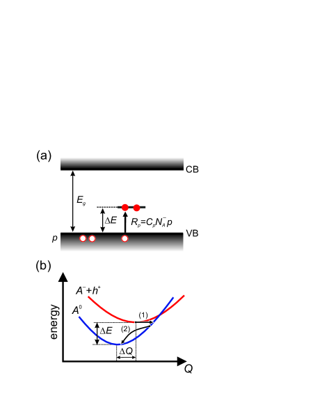
Without loss of generality, let us consider nonradiative carrier capture of a hole by an acceptor defect. The process is illustrated in Fig. 1 in two different representations: (a) a band diagram, and (b) a configuration coordinate (cc) diagram. In the latter, a one-dimensional generalized coordinate is used to represent atomic relaxations. Stoneham The excited state of the system corresponds to the negatively charged acceptor and a hole in the valence band (+), while the ground state corresponds to the neutral state of the acceptor (). The equilibrium geometries of the two charge states are different. is the energy difference between the two states.
Carrier capture consists of two elementary steps: an energy-conserving transition between two electronic states, process (1), and vibrational relaxation, process (2), in Fig. 1(b). Vibrational relaxation occurs on a timescale of a few picoseconds,Matulionis_APL_2009 while the electronic transition is much slower.Henry_PRB_1977 Thus, the electronic transition is the bottleneck for nonradiative capture, and in this work we will only consider process (1).
Let be the density of holes in the system. The total concentration of defects is , where is the density of negatively charged (ionized) acceptors, and is the density of neutral acceptors. The holes are captured at a rate Abakumov
| (1) |
where the units of are cm-3s-1; is the hole capture coefficient, with units =cm3s-1. An analogous equation applies to electron capture processes.
In principle carrier capture can occur both radiatively and nonradiatively. Huang_PRCL_1950 The two processes are in general competing and can occur simultaneously. The rate of radiative transitions increases with the energy of a transition as a power law; for semiconductors typical capture coefficients are of the order cm3s-1. Stoneham The dependence of nonradiative capture rates on the energy of the transition is usually nonmonotonic; capture coefficients can vary over a very wide range cm3s-1. Henry_PRB_1977 ; Stoneham When capture coefficients are in the upper part of this range, nonradiative transitions are dominant, and radiative transitions can be neglected. This is the case for all capture processes that we study in the present work.
The main goal of the theory is to determine nonradiative electron and hole capture coefficients and from electronic structure calculations. In the literature, carrier capture processes are often described in terms of capture cross sections . The two quantities are related via , where is a characteristic electron velocity. For non-degenerate statistics this velocity is the average thermal velocity. While and are more fundamental quantities, capture cross sections are useful because of their straightforward and intuitive interpretation. Experimental values for capture cross sections in a wide variety of systems Henry_PRB_1977 ; Stoneham vary between Å2 (weak coupling) and Å2 (very strong coupling).
III Theoretical formulation and computational methodology
III.1 Computational toolbox
To describe the atomic and the electronic structure of defects and bulk materials we use DFT with a hybrid functional. Heyd_JCP_2003 Hybrid functionals add a fraction of Fock exchange to the exchange described by the generalized gradient approximation, greatly improving the description of structural properties and band structures, including band gaps. Both of these aspects are particularly important for defects.Pacchioni_PRB_2000 ; Deak_JPCM_2005 ; Alkauskas_PRL_2008 ; Lyons_APL_2009 In addition, hybrid functionals can correctly describe the polaronic nature of anion-bound holes derived from N and O states, Pacchioni_PRB_2000 ; Lyons_APL_2009 ; Lyons_PRL_2012 ; Lyons_JJAP_2013 which is crucial for the defects in the present study.
We use the functional of Heyd, Scuseria, and Ernzerhof (HSE). Heyd_JCP_2003 In this functional the Fock exchange is screened (screening parameter = Å-1), and the sum rule for the exchange hole is fulfilled by suitably modifying the semilocal part of the exchange. We adapt the functional by tuning to reproduce the experimental band gaps, which has become a common procedure; Deak_JPCM_2005 ; Alkauskas_PRL_2008 ; Lyons_APL_2009 the corresponding values are = for GaN and = for ZnO. For = and = the HSE functional does not contain nonlocal exchange and is identical to the generalized gradient approximation functional of Perdew, Burke, and Ernzerhof (PBE). Perdew_PRL_1996
Our electronic structure calculations are based on the projector-augmented wave (PAW) formalism Bloechl_PRB_1994 , with PAW potentials generated at the PBE level. We have used the vasp code VASP with the implementation of hybrid functionals described in Ref. Paier_JCP_2006, . A kinetic energy cutoff of 29.4 Ry (400 eV) was used in all calculations. In the case of Zn, states were included in the valence. The resulting lattice parameters are = Å, = Å, and = for GaN (in excellent agreement with the experimental Madelung values 3.19 Å, 5.20 Å, and 0.377, respectively); and = Å, = Å, and = for ZnO (experimental Madelung values 3.25 Å, 5.20 Å, and 0.382).
Defects were modeled using the supercell methodology. VanDeWalle_JAP_2004 The defect calculations used 96-atom wurtzite supercells, with the lattice parameters optimized at the HSE level. In the calculation of formation energies of charged defects, as well as charge-state transition levels (ionization potentials), finite-size corrections as proposed in Ref. Freysoldt_PRL_2009, were included. The Brillouin zone was sampled at one special -point.Baldereschi_PRB_1973 For test systems, these calculations produce results for defect levels within 0.03 eV of those obtained with a mesh.
While most of our calculations were performed using the PAW methodology, it makes calculations of electron-phonon coupling matrix elements quite cumbersome. Such calculations are greatly facilitated within the plane-wave pseudopotential (PW-PP) formalism Ihm_JPC_1979 , which we adopted for this purpose. Norm-conserving Troullier-Martins pseudopotentials (PPs) Troullier_PRB_1991 were generated at the PBE level using the fhi98pp program. Fuchs_CPC_1999 states were included in the valence for both Zn and Ga. The energy cutoff for plane-wave expansion of wavefunctions was set to 80 Ry in GaN and 100 Ry in ZnO. We used the cpmd code, CPMD with the implementation of hybrid functionals discussed in Refs. Todorova_JPCB_2006, , Broqvist_PRB_2009, , and Komsa_PRB_2010, . Brillouin-zone sampling in these calculations was performed using a single point. In order to reproduce experimental band gaps, values of 0.38 for GaN and 0.47 for ZnO had to be used in these PP calculations, i.e., larger than in the PAW calculations. We attribute this to the generation of PPs at the PBE level, rather than consistently with hybrid functionals (cf. Refs. Alkauskas_PRL_2008, ; Broqvist_PRB_2009, ; Komsa_PRB_2010, ; Alkauskas_PRL_2008b, ; Wu_PRB_2009, ). However, for parameters for which direct comparisons can be made, such as total energy differences, equilibrium atomic configurations, or vibrational frequencies, the PW-PP calculations are in gratifyingly good agreement with the PAW results; for instance, charge-state transition levels for the defects considered here differ by 0.09 eV or less.
III.2 Derivation of the capture coefficient
Let us consider a hole capture process at a single acceptor, as in Fig. 1; the discussion can be easily adapted to other cases. Let be a large volume that contains holes, their density being , and the total number of hole-capturing defects in the appropriate negative charge state, with a density of =. The total density of defects is . Under non-equilibrium steady-state conditions, both electrons and holes can be present in the system. Mobile carriers screen the Coulomb potential of impurities, with a screening length . (For neutral impurities, would be the extent of their short-range potential.) A few distances away from each impurity the potential essentially vanishes. We will assume that , implying that the region where the potential is not negligible constitutes a very small part of the solid. Since the hole density near the impurity is obviously different from , this assumption means that the hole density in the space where the potential of impurity atoms can be neglected is equal to the average density, i.e., . A similar condition (i.e., ) allows us to assume that two holes do not interact with the same impurity at the same time.
Computationally the most convenient quantity to calculate is the capture rate of one hole at one defect in the whole volume . Let the capture rate for such process be (=s-1). The capture rate of holes at all identical defects (all in their negative charge states) in volume is then = (=s-1). We can rewrite this equation as . By comparing this equation with Eq. (1), and noting that, by definition is the capture rate per unit volume, we see that the hole capture coefficient is given by:
| (2) |
From now on consider only one hole being captured by one defect.
The general idea behind nonradiative processes due to multiphonon emission is closely related to the concept of electron-phonon coupling in bulk solids. Hedin_1970 We briefly review the main ideas, emphasizing the aspects specific to defects. The many-body Hamiltonian of the entire system of electrons and ions is
| (3) |
where represents kinetic energy, represents Coulomb interaction, and the subscript “e” is for electrons and “I” for ions. For an isolated system at zero temperature the solution of the Schrödinger equation yields the energy spectrum and many-body wavefunctions . represents all electronic degrees of freedom and represent all ionic coordinates (which can be transformed to phonon coordinates in the harmonic approximation). In most practical situations, however, it is more useful to describe the system not via eigenstates of the full Hamiltonian , but via eigenstates of a simpler Hamiltonian that encodes the essential physics of the system.Hedin_1970 Eigenstates of can be written as a product of the electronic and the ionic part. The term is then the perturbation that causes transitions between eigenstates of . These transitions should be rare in order to ensure that the Hamiltonian captures the essential physics of the system.Hedin_1970 The part of that is due to the ions and that induces transitions between different electronic states, such as in the case of nonradiative carrier capture, is the electron-phonon coupling . The remaining piece describes electron-electron and phonon-phonon interactions that are not discussed further.
The time scale associated with carrier capture processes in semiconductors is usually much larger than both phonon lifetimes and periods of lattice vibrations (an assumption that has to be verified a posteriori). As a result, the most convenient starting point to describe a coupled system of electrons and ions is the so-called static approximation. Paessler_pssb_1975 ; Peuker_pssb_1982 ; Goguenheim_JAP_1990 In this approximation, which we will adopt here, the total wavefunction of the system can be written as , where is the electronic wavefunction calculated for a chosen ionic configuration , and is the ionic wavefunction. The choice of will be discussed in Sec. III.6.
Let the many-body electronic wavefunction that describes a hole in the valence band (which is perturbed by the presence of the defect) and a negatively charged defect be . This is the excited (initial) electronic state. The electronic wavefunction that describes a hole trapped on a defect (yielding a neutral charge state of the center) is . This is the ground (final) electronic state. The associated ionic wavefunctions are and , where and are quantum numbers for ionic states.
At finite temperatures free holes occupy various electronic states according to the Fermi-Dirac or, in the non-degenerate case, the Boltzmann distribution. As a result, they cannot be described by a single initial state . The carrier capture rate that is experimentally measured is the weighted average over all initial electronic states. We adopt an approximation that charge carriers can be represented by a single initial electronic state; see Chapter 14.3 of Ref. Stoneham, for a more in-depth discussion. In the case of the non-degenerate hole or electron gas, this special state represents particles with a thermal velocity; in the degenerate case the special state represents particles at the Fermi surface.
In this work, we consider the interaction within the first order of electron-phonon coupling. Under this assumption, the capture rate that enters into Eq. (2) is given by Fermi’s golden rule (see, e.g., Sec. 14.2 of Ref. Stoneham, ):
| (4) |
Here is the thermal occupation of the vibrational state of the excited electronic state, and and are total energies of the initial and the final vibronic state. is the degeneracy factor of the final state; it reflects the fact that there might exist a few equivalent energy-degenerate (or nearly degenerate) atomic configurations of the final state. For example, the neutral charge state of Li in ZnO can correspond to four different lattice relaxations in which the hole is localized on one of the four surrounding oxygens,Du_PRB_2009 ; Carvalho_PRB_2009 ; Bjorheim_JPCC_2012 ; Lyons_2014 yielding . Similarly, for GaN:C.Lyons_APL_2009 We do not distinguish between axial and azimuthal configurations in the wurtzite structure. In the equation above, is the electron-phonon coupling matrix element. In the static approach,Paessler_CJP_1982 ; Paessler_pssb_1975 .
To make the problem more tractable, subsequent approximations need to be employed. The first of those is the linear-coupling approximation. Stoneham In this approximation is Taylor-expanded in around (see Sec. III.6), and only the first-order terms are retained. The matrix element is then given by:
| (5) |
The sum runs over all phonon modes , and is the projection of the initial atomic configuration along each of the phonon coordinates. is the electron-phonon coupling matrix element pertaining to the phonon . Equations (2), (4) and (5) form the starting point for our computational determination of .
III.3 Vibrational problem
The approximations introduced so far are fairly standard and have been employed in previous work. Abakumov ; Paessler_pssb_1975 ; Peuker_pssb_1982 ; Goguenheim_JAP_1990 Here we introduce an additional approximation, relating to the phonon coordinates, which will turn out to be essential for making the calculations of electron-phonon matrix elements feasible. In particular, we will consider only one special phonon mode that replaces the sum over all vibrational degrees of freedom in Eq. (5). The choice of the phonon mode is motivated by the following reasoning. We are dealing with deep levels, with ionization energies that are usually many times larger than the energy of the longitudinal optical phonon (which has the largest energy of all phonon modes). This is the reason why a single phonon process is not sufficient to couple the two electronic states, and a MPE is necessary. The phonons that contribute most to the the sum in Eq. (5) are those that couple most strongly to the distortion of the defect geometry during the carrier capture process. This is ensured by the second factor in Eq. (5), since this expression vanishes for those modes that do not couple to this distortion.
This approach is supported by results that have been obtained in the case of radiative transitions. In the case of luminescence at defects with strong electron-phonon interactions, as quantified by their Huang-Rhys factors Huang_PRCL_1950 , it is possible to show numerically that replacing many participating phonon coordinates with one carefully chosen effective phonon mode is an excellent approximation. Alkauskas_PRL_2012 This conclusion is in line with an empirical finding that it is often possible to describe the temperature dependence of broad defect luminescence bands considering only one effective vibrational degree of freedom Stoneham ; Reshchikov_JAP_2005 . This special mode corresponds to an effective vibration Schanovsky_JVST_2011 ; Alkauskas_PRL_2012 where the displacement of an atom along the direction = is proportional to =, where are atomic coordinates in the equilibrium configuration of the excited (initial) and the ground (final) state. In this one-dimensional model the generalized configuration coordinate for values of atomic positions that correspond to this displacement is
| (6) |
where are atomic masses. The geometry of the ground state (final state ) corresponds to =0, while the geometry of the excited state (initial state ) corresponds to = with
| (7) |
In this description the configuration coordinate of Eq. (6) has units of amu1/2Å (amu - atomic mass unit). We will give a brief description of changes of the defect geometry encoded in when discussing specific systems in Section IV. The plot that shows the total energies in the ground and the excited states as a function of is called the configuration coordinate diagram (cc diagram) Stoneham ; we have shown a schematic example in Fig. 1(b). The frequency of the effective vibration in the ground and the excited state is given as
| (8) |
An auxiliary quantity =, allows to define the modal mass of the vibration via =. Schanovsky_JVST_2011 The knowledge of is useful for interpreting the value of for different defects.Alkauskas_PRL_2012 A very useful dimensionless quantity is the Huang-Rhys factor, defined as Huang_PRCL_1950 ; Alkauskas_PRL_2012
| (9) |
The case corresponds to large lattice relaxations associated with the change of the charge state. We note that the special mode is not an eigenstate of the vibrational Hamiltonian, but it serves as a very useful approximation and has a clear physical meaning. Possible errors introduced by the use of the one-dimensional approximation are critically reviewed in Sec. V.2.
III.4 Electron-phonon matrix elements
Thanks to the one-dimensional (1D) approximation described in Sec. III.3 we have to determine only a single electron-phonon coupling matrix element:
| (10) |
At this stage, are still many-electron wavefunctions, and is the many-body Hamiltonian of the system. In an independent-particle picture corresponding to the (generalized) Kohn-Sham approach of DFT, we will assume that the many-body Hamiltonian and many-electron wavefunctions in Eq. (10) can be replaced by their single-particle counterparts and , i.e.:
| (11) |
Whereas wavefunctions describe the entire electronic system, single-particle wavefunctions have a different meaning: corresponds to the hole in the valence band perturbed by the presence of the defect, and is the localized defect state. Indeed, for perturbation theory to be physically meaningful, both states have to be eigenstates of the same Hamiltonian: the initial state has to correspond to the perturbed hole state rather than a hole state in an unperturbed bulk material.
To calculate electron-phonon matrix elements we use hybrid functionals within the PW-PP approach, as discussed in Sec. III.1. Therefore, contains nonlocal Fock exchange, as well as the nonlocal part of pseudopotentials. These terms would have to be calculated explicitly if Eq. (11) were used. To avoid such a cumbersome procedure, it is extremely convenient to use an alternative expression that follows directly from perturbation theory [e.g., Eq. (28) in Ref. Baroni_RMP_2001, ]:
| (12) |
In this expression the main effort in calculating the matrix element boils down to the calculation of the derivative . This is accomplished by evaluating the derivative numerically via finite differences, as discussed for specific defects in Sec. III.6.
III.5 Bulk scattering states
The methodology outlined in Sec. III.2 above relies on calculating the capture rate for one hole, with a finite velocity, at one defect in the entire (large) volume . The role of all other carriers is to screen the long-range Coulomb interaction between the hole and the defect. The electron-phonon coupling matrix element for one special phonon mode is determined via Eq. (12), and the capture coefficient is subsequently determined via Eqs. (2), (4) and (5). Only one phonon coordinate is retained in expression (5).
The problem with this formulation is the following. Actual calculations are performed for a system with a relatively small volume, the supercell with a volume that is constrained by computational limitations. While there is plenty of evidence that the localized defect state is accurately represented in such supercell calculations, this is not necessarily the case for the initial perturbed bulk state . In particular, if the capturing center is charged, the screened Coulomb interaction between the defect and the carrier significantly affects the capture processes. Such interactions are not well represented in the supercell calculation. Let us picture, as an example, a charged carrier with a vanishing kinetic energy being captured at a repulsive center. As the size of the system grows, the particle is expelled further and further away from the defect. In the limit of an infinite volume , and zero kinetic energy of the charge carrier, the capture rate would tend to zero. However, in the supercell of volume the carrier cannot be expelled to infinity, and the capture rate remains finite, which is an incorrect physical result. Similar considerations also apply to attractive centers and emphasize the need of the correction term, which we discuss here.
Let the electron-phonon coupling matrix element calculated in the computational supercell be . It is calculated via the equation, similar to Eq. (12):
| (13) |
Here, is the bulk wavefunction in the supercell of volume , chosen to be at the point of the supercell. Let the corresponding carrier capture coefficient, determined via equations analogous to Eqs. (2)-(5), whereby all the parameters of the real system are substituted with corresponding values from the supercell calculation, be . Similar to the procedure proposed in Refs. Bonch-Bruevich_FTT_1959, and Paessler_pssb_1976, we express the actual capture coefficient as
| (14) |
where is a dimensionless scaling factor that depends on the reference calculation used to determine the matrix element , the charge state of the defect, as well as environmental parameters: electron density , hole density , and temperature . Bonch-Bruevich Bonch-Bruevich_FTT_1959 and later Pässler Paessler_pssb_1976 provided analytic expressions of for both repulsive and attractive centers. In the present Section we derive an expression of in the context of our supercell approach. Our analysis follows that of Pässler,Paessler_pssb_1976 but is adapted for use in conjunction with supercell calculations of defects.
The function can in principle be constructed using a first-principles approach. However, such a calculation would be very cumbersome and not particularly useful at this point, keeping in mind that other, more limiting approximations have already been made. Instead we employ a model calculation to determine .
Let us assume that the perturbed bulk wavefunction in the real physical system can be described as a product of the wavefunction that reflects the atomic-scale behavior and the envelope wavefunction that changes on a scale larger than the unit cell: . We chose the normalization condition for to be the same as for . is a fast-varying dimensionless function. Such a description is in the spirit of the effective-mass approximation.Kohn_PR_1957 The electron-phonon coupling matrix element can then be expressed as
| (15) |
where is the value of the envelope wavefunction at the defect site, and a new matrix element was introduced. According to the methodology described in Secs. III.2, III.3, and III.4 [Eqs. (2), (4), (5), (11), and (15)] the capture coefficient is then proportional to
| (16) |
Here, is the large volume of the material introduced in Sec. III.2. In the region where the potential of impurities is negligible . Because of the interaction with the impurity, can have a different value.
Let us assume that the perturbed bulk state in the computational supercell can also be written in terms of a similar product, i.e., . Because of its localized nature, the defect wavefunction is the same in the supercell of volume as in a large volume . By definition, the same holds for the “atomic” part of the bulk wavefunction . As a result,
| (17a) | ||||
| (17b) | ||||
Accordingly:
| (18) |
Therefore, from Eqs. (14), (16), and (18):
| (19) |
In practice, we use the following procedure. The value is determined by considering a scattering problem for a particle with a finite momentum , Landau which we take to be the thermal momentum for the non-degenerate case. Far from the scattering center the wavefunction is normalized as required by the formulation of our problem ( for ). Within the -wave approximation,Landau the value of the wavefunction at the origin is determined by a numerical integration of the Schrödinger equation for the =0 angular momentum component of the scattering wavefunction with an asymptotic form that corresponds to our normalization. The scattering potential that we use is
| (20) |
Here is the low-frequency dielectric constant of the host material, is the extent of the defect wavefunction, and is the screening length due to the presence of other charge carriers, as discussed at the beginning of Sec. III.2. In the case of a non-degenerate gas we use the Debye-Hückel screening length that depends on and on the carrier densities , , explaining the overall dependence of on these parameters. At room temperature, the hole gas is non-degenerate up to densities of cm-3 in both GaN and ZnO.
The value of is obtained by consideration of the scattering problem with the potential in Eq. (20). We determine by comparing the behavior of the bulk wavefunction in the presence of a charged defect in the actual supercell calculation with the wavefunction obtained from a model supercell calculation within the effective-mass approximation. is chosen so that the behavior of the envelope wavefunction in the model supercell calculation accurately represents the behavior of the envelope function in a real calculation. This model supercell calculation also yields the value of .
For an attractive Coulomb potential the problem can be solved analytically.Landau ; Paessler_pssb_1976 When , where is the effective Bohr radius in the material, (see Eq. (4.4) in Ref. Paessler_pssb_1976, ). We find numerically that a similar form describes very accurately the behavior of carriers also for the potential of the form Eq. (20) when the center is attractive (). We find that depends very weakly on , which in its turn depends on carrier density, and thus we can use density-independent scaling function. In our formulation is the average thermal momentum of holes and is a constant. For the non-degenerate hole gas ( is the Boltzmann constant), and thus the scaling function depends only on temperature:
| (21) |
where is a constant determined numerically. For the two attractive centers considered in the present study (GaN:C and ZnO:Li) we found K1/2 when the electron-phonon matrix element is determined for a neutral charge state for reasons discussed in Sec. III.6. In the scattering problem, we assumed effective hole masses = for GaNPankove_1975 ; Santic_SST_2003 , and 0.6 for ZnO.Hummer_PSS_1973 For attractive centers and temperatures considered in this work ( K) .
This result is intuitive and can be explained as follows. Close to the defect the wavefunction of the hole has a larger amplitude with respect to its asymptotic value far away from the defect; in the classical reasoning, the hole spends more time near the defect due to Coulomb attraction. The function reflects this enhancement. For example, the factor is about 10 at room temperature.
The third defect considered in our work, GaN:(Zn-), captures holes in a neutral charge state (see Sec. IV.3), thus there are no long-range Coulomb interactions between the defect and the hole. However, the electron-phonon coupling matrix element is calculated in the positively charged state (96-atom supercell), as discussed in Sec. III.6. In this case we find . This implies that in the supercell calculation the hole is repelled from the defect more than in the actual situation.
In the case of repulsive centers depends sensitively both on temperature () Bonch-Bruevich_FTT_1959 , and on the density of charge carriers. Repulsive centers are not considered in this work.
III.6 Initial state for perturbation theory
The actual quantity that is calculated is the capture coefficient that corresponds to our computational setup. The expression can be derived from Eqs. (2), (4), and (5), whereby all quantities correspond to the parameters in the supercell calculation (rather than the actual system) and only one phonon mode is retained in Eq. (5):
| (22) |
is given via Eq. (13). For numerical evaluation, the function is replaced by a smearing function of finite width, a practice also employed in calculating luminescence lineshapes. Alkauskas_PRL_2012 In this section we address the following questions: (i) which atomic configuration should we choose as a starting point for perturbation theory and (ii) for which charge state should we calculate the electron-phonon matrix element in Eqs. (13) and (22)?
During a nonradiative process the carrier in a delocalized state is captured to a localized defect state. Thus, in the configuration a single-particle defect level should be well defined and be in the bulk band gap. This is the single most important criterion for the choice of . Let us consider acceptor defects GaN:C and ZnO:Li as an example. As before, we study the capture of a hole by a negatively charged acceptor [process (1) in Fig. 1(b)]. Actual first-principles calculations show that in the case of neutral acceptors in their equilibrium geometries there is indeed one clearly distinguishable empty defect level in the band gap, representing a trapped hole. In contrast, in the case of the negatively charged defect in its equilibrium geometry the supercell calculation produces one or more diffuse single-particle defect states that have moved down in energy and that couple strongly with bulk states. However, when the calculation is performed for the same negatively charged acceptor but rather in the equilibrium geometry of the neutral system, one doubly-occupied single-particle defect state moves up in energy and into the band gap. A defect state to which the hole is being captured can be clearly identified again. The bottom line is that, when corresponds to the equilibrium geometry of the neutral charge state, a single-particle defect state can be clearly identified in both the neutral and the negative charge states. This choice of thus yields good single-particle wavefunctions for perturbation theory.
For this particular choice of the electron-phonon coupling constant can be then calculated for either the neutral or the negatively charged state. We find that the values calculated for the two states differ by about 5%. However, a different charge state for the calculation of the electron-phonon coupling matrix element yields a different scaling function , as discussed in Sec. III.5 [Eq. (19)]. In the end, the calculated capture rates are within 1% of each other. This result is reassuring, and also tells us something about the physics: the defect wavefunction does not change much when the defect state is filled with an electron.
If the band structure is such that the highest occupied states correspond to several closely spaced valence bands (which is the case for the most commonly used semiconductors) attention needs to be devoted to the choice of the valence band that represents the hole wave function. For example, the highest occupied states at the zone center of wurtzite-phase semiconductors, such as GaN and ZnO, consist of the heavy-hole (HH), light-hole (LH), and crystal-field split-off (CH) bands.Piprek The splitting between LH and HH is mainly due to the spin-orbit interactions, and is only a few meV for these two materials. Crystal-field effects are larger, and the CH band is 20 meV below the valence-band maximum (VBM) in GaN, and 60 meV in ZnO. Yan_SST_2011 Strain or effects of confinement in quantum wells could modify the splitting and ordering of these bands, and in an actual sample, the density of holes in each band is determined by the thermal occupation. For example, in bulk ZnO the CH band will be much less populated with holes than the other two bands at room temperature, and this can be relevant experimentally (see Sec. IV.2). Since we do not know a priori which valence band(s) will play the most important role in specific experimental situations, we explicitly calculate the electron-phonon coupling to all three valence bands in the supercell.
The use of the supercell itself introduces an additional complication, since the splitting between the bands and their ordering can be significantly affected by the defect. We find that the valence band that interacts most strongly with the defect state is always pushed below the other two bands. However, while the precise energetic position of the bands may be affected, we find that the character of the valence bands is generally retained in defect supercells, allowing us to meaningfully calculate the electron-phonon coupling matrix elements for the separate valence bands. While these matrix elements could in principle be explicitly employed in calculations that reflect specific experimental conditions, for purposes of reporting our results in the present paper the matrix element of Eq. (10) that enters into the final calculations is defined as the mean-square average of the three separate matrix elements.
Here, we illustrate the calculation of for two specific defects, C in GaN and Li in ZnO. The calculation of the electron-phonon matrix element using Eq. (13) is shown in Fig. 2. Panel (a) shows the single-particle eigenvalues as a function of a generalized coordinate , where , corresponding to the geometry of the neutral defect state, is set to 0. The eigenvalues are referenced to the VBM. In the case of a defect immersed in infinite bulk the eigenvalues of bulk states should not be dependent on . This condition is fulfilled in our supercell calculations [Fig. 2(a)]. In contrast, the defect state shows a pronounced linear dependence on . For the calculation of the value of at is taken.
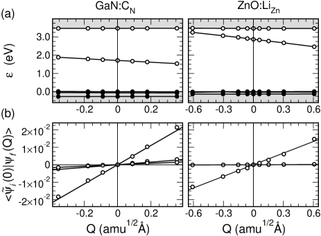
In Fig. 2(b) the overlap integral is plotted as a function of for all three valence bands. The derivative used for the calculation of the matrix element in Eq. (13) was determined from a linear fit to this dependence. The coupling to one of the three valence bands can be as much as two orders of magnitude larger than for the other bands, as discussed above.
III.7 Brief summary of the methodology
To recap, we determine the carrier capture rate that is specific to our supercell geometry using Eq. (22). is the volume of the supercell; is the degeneracy of the final state; are electron-phonon coupling matrix elements, given in Eq. (13) [cf. Fig. 2]; is the energy difference between the ground and excited state that is given by the position of the charge-state transition level above the VBMVanDeWalle_JAP_2004 ; == is chosen to correspond to the equilibrium atomic configuration of the ground state; the equilibrium atomic configuration of the excited state is offset by = [Eq. (7)]. All these quantities are summarized in Table 1. In addition, we provide Huang-Rhys factors [Eq. (9)]. -functions in the sum Eq. (22) are replaced by Gaussians with widths =.Alkauskas_PRL_2012
Finally, the actual carrier capture coefficient is obtained via [Eq. (14)] with the scaling function . As discussed in Sec. III.5, the calculation of may require a simulation in its own right; for the case of hole capture by a negatively charged defect, when the reference system is that of the neutral charge state, we use the form Eq. (21) for . This is the situation that occurs in the examples of GaN:C and ZnO:Li, to be discussed in Secs. IV.1 and IV.2. For the case of hole capture by a neutral defect, which applies to GaN:(Zn-) to be discussed in Sec. IV.3, the reference system is that of a positive charge state and for our particular supercell.
| (amu1/2Å) | (eV) | (meV) | (meV) | (eV/amu1/2Å) | (Å3) | ||||
|---|---|---|---|---|---|---|---|---|---|
| Defect | theory | expt. | |||||||
| GaN:C | 1.61 | 1.02 (this work) | 0.85111Ref. Demchenko_PRL_2013, | 42 () | 36 (0) | 10 | 4 | (0) | 1100 |
| ZnO:Li | 3.22 | 0.80222Ref. Carvalho_PRB_2009, , 0.49333Ref. Bjorheim_JPCC_2012, , 0.46444Ref. Lyons_2014, | 0.53555Ref. Reshchikov_PB_2007, | 36 () | 25 (0) | 28 | 4 | (0) | 1136 |
| GaN:(Zn-) | 3.33 | 0.90666Ref. Shi_PRL_2012, , 0.88 (this work) | 26 (0) | 22 (+) | 30 | 1 | () | 1100 | |
IV Results
To illustrate our methodology, we study two defects in GaN, namely carbon on the nitrogen site (GaN:C) and a complex of zinc on a gallium site with a nitrogen vacancy (GaN:(Zn-)), as well as one defect in ZnO, namely lithium on the zinc site (ZnO:Li). Experimental identification of defects is often very difficult and frequently controversial. In order to check our methodology, we wanted to identify benchmark cases where the experimental situation is clear-cut. GaN:C and ZnO:Li serve this purpose.
Although the focus is on nonradiative transitions, luminescence experiments are frequently used to analyze rates of the various processes, radiative as well as nonradiative. There is general consensus that GaN:C gives rise to a yellow luminescence band, Ogino_JJAP_1980 ; Seager_JL_2004 ; Lyons_APL_2010 and ZnO:Li to an orange luminescence band.Meyer_pss_2004 ; Lyons_2014 These two bands arise due to the recombination of an electron in the conduction band and a hole bound to a defect. In both of these cases the acceptor level is in the lower part of the band gap.
Nonradiative hole capture rates for deep acceptors can be determined from luminescence experiments in the following way.Reshchikov_PL_2012 In -type samples photo-generated holes are captured by acceptors in a predominantly nonradiative process (this conclusion stems from the fact that the resulting capture rates are orders of magnitude higher than possible radiative capture rates, as discussed in Sec. II). Subsequently, these captured holes recombine with electrons in the conduction band, a process believed to be predominantly radiative, giving rise to the aforementioned luminescence bands.Reshchikov_PL_2012
When the temperature is increased, the radiative transition is quenched because captured holes are re-emitted back into the valence band. Therefore, the measurement of the thermal quenching of a particular luminescence band as a function of temperature provides information about the hole emission coefficient . The parameters needed to determine using this procedure are the radiative lifetime , measured separately from time-dependent photoluminescence decay, and the quantum efficiency of the band with respect to all other recombination channels. Reshchikov_PL_2012 The hole capture coefficient is determined from using the detailed balance equation. Abakumov ; Reshchikov_PL_2012 For acceptors in GaN and ZnO nonradiative hole capture coefficients determined in this way are summarized in Ref. Reshchikov_AIP_2014, .
The GaN:(Zn-) defect, finally, has been included in order to compare our approach to that of Ref. Shi_PRL_2012, , where nonradiative hole capture at this defect was studied.
IV.1 C in GaN
IV.1.1 GaN:C and yellow luminescence
Carbon is one of most abundant impurities in GaN, especially if grown by metal organic chemical vapor deposition, where organic precursors are used. A clear link has been established Ogino_JJAP_1980 ; Seager_JL_2004 between the concentration of carbon and the intensity of a yellow luminescence (YL) band that peaks at about 2.2 eV. Contrary to earlier suggestions of carbon being a shallow acceptor, Lyons et al. have shown, using hybrid density functional calculations, that carbon on the nitrogen site is in fact a deep acceptor. Lyons_APL_2010 Calculations Lyons_APL_2010 ; Demchenko_PRL_2013 ; Lyons_PRB_2014 yield a charge-state transition level =0.9-1.1 eV above the VBM. In conjunction with a large lattice relaxation this corresponds to a peak very close to 2.2 eV for the optical transition whereby a neutral defect captures an electron from the conduction band. Recently we have employed first-principles calculations to determine effective parameters (average phonon frequencies and the Huang-Rhys factors, see Sec. III.3 and Table 1) that describe the shape and temperature dependence of luminescence bands. In the case of C excellent agreement with experimental results Ogino_JJAP_1980 ; Reshchikov_AIP_2014 was demonstrated. Alkauskas_PRL_2012
IV.1.2 Configuration coordinate diagram
A 1D cc diagram relevant for the capture of holes at GaN:C is shown in Fig. 3. The excited state corresponds to the defect in the negative charge state and a hole in the valence band, and the ground state corresponds to a neutral charge state. The configuration coordinate was described in Sec. III.3, and is the same as used in our calculations of luminescence lineshapes. Alkauskas_PRL_2012 In the case of GaN:C,Lyons_APL_2010 the biggest contribution to comes from the the relaxation of C and Ga atoms, which results in the shortening of C-Ga bond lengths by Å, as the charge state changes from neutral to . A smaller contribution comes from the relaxation of next-nearest N atoms, which results in a slight increase of C-N distances, expected from electrostatic arguments. Potential energy surfaces in the two charge states were mapped along this configuration coordinate. The separation between the minima of the two potential energy surfaces corresponds to the energy of the charge-state transition level with respect to the VBM. Our calculated value for =1.02 eV is slightly larger than the one reported in Ref. Lyons_APL_2010, due to more stringent convergence criteria. The minima of the two potential energy surfaces are offset horizontally by =1.61 amu1/2Å [Eq. (7)]. An important parameter is the relaxation energy in the ground state [Fig. 3]. For calculations yield =0.37 eV.
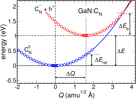
The two potential energy curves intersect at =0.73 eV above the minimum of the excited state. We might thus expect that the nonradiative carrier capture is a temperature-activated process, since the coupling between two potential energy surfaces is always most efficient close to the crossing point.DiBartolo
IV.1.3 Calculated hole capture coefficients
The real situation is not so straightforward because of the occurrence of two competing factors. On the one hand, when the temperature is raised, higher-lying vibrational levels of the excited electronic state [see Eqs. (4) and (22)] become populated. Vibrational levels that are closer in energy to the crossing point of the two potential energy curves yield larger contributions to the overall rate. Thus, if this was the only factor, the nonradiative capture rate for GaN:C would increase as a function of temperature. On the other hand, however, the scaling factor decreases with temperature, as per Eq. (21), because an increasingly faster hole has less chance of being captured by a negative acceptor.
It is instructive to consider the first effect separately. In Fig. 4 we show the calculated nonradiative hole capture rate if the second effect is completely neglected, i.e., for . This is the capture rate that is discussed in Section III.5. The process is indeed temperature-activated. At high temperatures, the dependence is often fitted to a function of the form
| (23) |
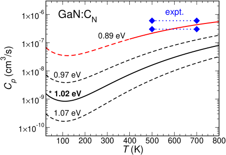
with a temperature-independent part and a temperature-activated part. The use of such a form is at the core of the famous Mott-Seitz formula for temperature quenching of luminescence bands. DiBartolo The fit is shown in Fig. 4. From the fit one can derive an effective barrier =0.23 eV, which is significantly smaller than the “classical” barrier =0.73 eV. This is a typical result and happens because of the quantum-mechanical tunneling DiBartolo that is considered in the quantum treatment but absent in a classical description.

The actual hole capture coefficient, including the scaling factor [Eq. (21)], is presented in Fig. 5 (solid black line). At =300 K, our calculated value is cm3s-1. To determine the sensitivity of the final result on the parameters of our calculation, we have also determined the capture coefficient for =1.020.05 eV (Fig. 5). A change in by just 0.05 eV translates into a change of by a factor of (black dashed lines in Fig. 5). Since (cf. Fig. 3), larger values of yield larger barriers and therefore smaller capture coefficients . The strong dependence of nonradiative transitions on is well documented,DiBartolo and was recently emphasized again in Ref. Shi_PRL_2012, . This sensitivity stems from the temperature-activated behavior discussed in the preceding paragraphs. We can consider the range of capture coefficients shown in Fig. 5 to represent a theoretical “error bar” regarding the 0 K value of that is used in the calculation.
IV.1.4 Comparison with experiment
In Refs. Reshchikov_AIP_2014, and Demchenko_PRL_2013, the hole capture coefficient for CN was determined in the temperature range 500-700 K, at which quenching of the luminescence occurs. was assumed to be weakly dependent on temperature in this range, and the values obtained for different samples were and cm3s-1.Reshchikov_AIP_2014 These results are shown by horizontal dotted lines and diamonds in Fig. 5. At =600 K, i.e., the midpoint of the 500-700 K temperature range where the quenching occurs, our calculated value for eV is cm3s-1, i.e., about an order of magnitude smaller than the experimental result. The corresponding values for =0.97 eV and 1.07 eV are and cm3s-1 (cf. Fig. 5). Thus, variations of by 0.05 eV do not remove the difference between theory and experiment.
The apparent discrepancy between experiment and theory can be explained as follows. The calculated of 1.02 eV corresponds to the ionization potential of the C acceptor at =0 K, while the comparison with experiment is made for 600 K. At 600 K the bulk band gap of GaN shrinks from its =0 K value of 3.50 eV to about 3.24 eV. Nepal_APL_2005 This decrease of the band gap will affect the ionization potential of the acceptor. We are not in a position to address this fully from first principles, but we can obtain a zero-order estimate of the effect of temperature on by assuming that (i) the charge-state transition level remains the same on the absolute energy scale when the band gap changes,Alkauskas_PRL_2008 ; Lyons_PRB_2014 ; Chen_PRB_2013 and (ii) the VBM and the conduction-band minimum are equally affected, i.e., that as a function of temperature they move symmetrically on the same absolute energy scale. Based on these assumptions we estimate a decrease of the ionization potential by about eV in going from 0 K to 600 K. In Fig. 5 we have included a curve for as a function of for =0.89 eV (red solid and dashed curve). This curve is physically meaningful only at temperatures around 600 K, corresponding to a significantly reduced value of . At =600 K, the calculated value cm3s-1 is in excellent agreement with the experimental data. Reshchikov_AIP_2014 ; Demchenko_PRL_2013
We thus find that significant variations of the calculated can result from the temperature dependence of . For comparison with experiments carried out at elevated temperatures this can make a difference in of about an order of magnitude. This dependence has not been studied in the past, neither theoretically nor experimentally. Our findings indicate that this will be a fruitful area of future work on nonradiative carrier capture. However, even in the absence of a rigorous analysis of the temperature dependence, we can conclude that our calculated values of are in very good agreement with experimental data.
IV.2 Li in ZnO
IV.2.1 ZnO:Li and orange luminescence
Li in ZnO is one of the most studied defects in ZnO. While it was initially hoped that Li might be a shallow acceptor leading to -type doping, it is now clear that this defect is a very deep acceptor. Meyer et al. suggested that Li gives rise to a broad orange luminescence (OL) band peaking at about 2.1 eV. Meyer_pss_2004 The ionization energy was deduced to be at least 0.5 eV. The analysis based on the thermal quenching of luminescence lines confirms this and yields values for the ionization potential eV; Reshchikov_PB_2007 ; Reshchikov_AIP_2014 the different values are for different ZnO samples. Recent theoretical work based on the application of the generalized Koopman’s theorem Lany_PRB_2009 and on hybrid density functionals Du_PRB_2009 ; Carvalho_PRB_2009 ; Bjorheim_JPCC_2012 ; Lyons_2014 has confirmed that Li is indeed a deep acceptor with a ionization energy 0.3 eV. The neutral charge state of the defect corresponds to a small polaron bound to an oxygen atom that is adjacent to Li.
IV.2.2 Configuration coordinate diagram
The calculated 1D cc diagram relevant for hole capture by a Li defect in ZnO is shown in Fig. 6. The calculations were consistently performed with the HSE hybrid functional (mixing parameter =) and resulted in a value =0.46 eV. Lyons_2014 In the negatively charged state the defect posses a C3v symmetry, with the axial Li-O bond-length of 2.00 Å, being only slightly larger than azimuthal Li-O bond-lenghts of 1.96 Å. In the neutral charge state the Li atom undergoes a huge relaxation Du_PRB_2009 ; Carvalho_PRB_2009 ; Bjorheim_JPCC_2012 ; Lyons_2014 of about 0.4 Å. This results in the increase of one of the Li-O bond-lengths to 2.61 Å, and the decrease of the remaining three to about 1.87 Å. The hole is bound to the oxygen atom involved in the long bond;Carvalho_PRB_2009 ; Bjorheim_JPCC_2012 ; Lyons_2014 three Zn atoms closest to this oxygen relax outwards by about 0.16 Å.
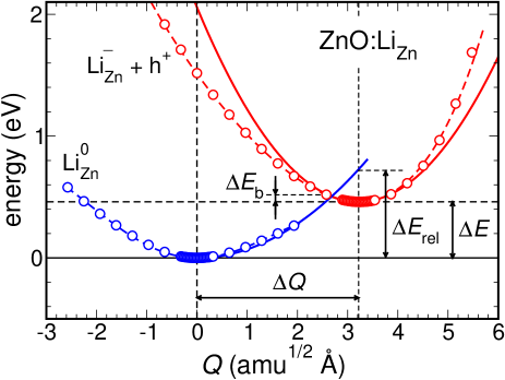
Note, that in contrast to GaN:C, in the case of ZnO:Li . Therefore, the two potential energy curves intersect for . Another difference with GaN:C is that the potential energy curves for ZnO:Li are very anharmonic. The solid curves in Fig. 6 present parabolic fits to the potential energy values, while dashed lines are fits to a fourth-order polynomial. We need to make an important point here: while we use the harmonic approximation in the present work, there is no requirement that the parabolic fit to the potential energy surface be performed for the entire range of values. Indeed, in order to capture the most essential physics we should focus on those values that are relevant for the transitions under investigation, i.e., the range of values where the potential energy curves cross. Therefore, in Fig. 6, the potential energy curve for the neutral charge state has been fitted to a parabolic curve only for . The effective phonon frequencies derived from the parabolic fits are included in Table 1.
IV.2.3 Calculated hole capture coefficients and comparison with experiment
The calculated hole capture coefficient for Li in ZnO is shown in Fig. 7 (black solid curve). Our room-temperature value is =1.3 cm3s-1. In Ref. Reshchikov_AIP_2014, the capture coefficient was determined from the quenching of the OL. The quenching occurred in the temperature range 225-300 K, and fitting yielded values cm3s-1, as indicated in Fig. 7 (diamonds and horizontal dashed line). To determine the sensitivity of the final result on the value of , we have calculated for =0.460.05 eV. As seen in Fig. 7, changes in by 0.05 eV result in changes in by about a factor of 2. However, in contrast to GaN:C, smaller yield larger values. This can be understood by considering the 1D cc diagram in Fig. 6. Since for all three values of , larger yield smaller barriers , and thus larger capture coefficients .
The temperature dependence of that was important for GaN:C at 600 K, is not substantial for ZnO:Li at 300 K. At 300 K the band gap of ZnO is lower by about 0.03 eV compared to its 0 K value. Considerations similar to the one performed for GaN:C would yield a change in by 0.015 eV, translating into a change of by at most 10%.
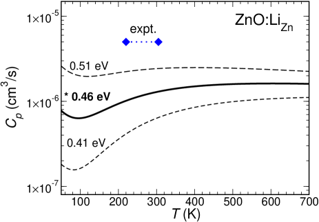
Both theory and experiment thus confirm that the coefficient for ZnO:Li is larger than that for GaN:C by about an order of magnitude. The main reason is the fact that the potential energy curves for ZnO:Li intersect close to the minimum of the excited state (Fig. 6), rendering the nonradiative process more likely even at low temperatures. In addition, we find that the temperature dependence of is significantly weaker for ZnO:Li than in the case of GaN:C. This is because the “classical” barrier for the nonradiative transition is very small for ZnO:Li (Fig. 6).
Overall, we can again conclude that first-principles calculations of hole capture coefficients at ZnO:Li agree very favorably with experimental data.
IV.3 Zn- in GaN
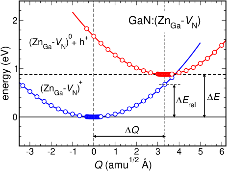
IV.3.1 Defect properties and configuration coordinate diagram
To compare our methodology with the approach used in Ref. Shi_PRL_2012, , we have also studied hole capture by a neutral Zn- complex in GaN, the example that was studied in that work. In contrast to GaN:C and ZnO:Li, GaN:(Zn-) is a deep donor with and charge-state transition levels in the lower part of the band gap. Its defect wavefunction is derived mostly from Ga states. To the best of our knowledge, no direct experimental data is available for this defect.
The approach of Shi and Wang is based on the adiabatic approach to nonradiative transitions, employing the formula derived by Freed and Jortner. Freed_JCP_1970 This should be contrasted to the static approach used in the current work. The distinction between the two approaches will be discussed in Section V.3. The calculation of Ref. Shi_PRL_2012, includes the coupling to all phonon modes.
A 1D cc diagram for Zn-, relevant for hole capture by a neutral center, is shown in Fig. 8. The values are again calculated with a hybrid functional with . With respect to the neutral charge state, four cation atoms surrounding the vacancy experience and outward relaxation in the positive chare state: Ga atoms relax by about 0.20 Å, while the Zn atom relaxes by about 0.12 Å. A relaxation away from the vacancy in the positive charge state is consistent with electrostatic arguments.
Our calculated value of =0.88 eV, corresponding to the (0/+) charge-state transition level, was used in Fig. 8. Our calculated value is close to the value =0.90 eV of Shi and Wang, Shi_PRL_2012 but this agreement is to some extent accidental, since the details of the calculations differ: Shi and Wang’s value was determined based on a supercell of 300 atoms, without any finite-size correction, using HSE calculations with but based on atomic geometries determined at the PBE level. We estimate that their value after inclusion of finite-size corrections would be 0.82 eV. As a check we performed the calculations using the hybrid functional with . Using the geometry obtained at the HSE level we obtain a value of eV for the charge-state transition level. If instead the geometry is obtained at the PBE level, the value is eV.
IV.3.2 Hole capture coefficients
In Fig. 9 we compare the results of Shi and Wang Shi_PRL_2012 with our present results. Shi and Wang’s values of are presented as a function of for two different values of , namely 0.6 and 1.0 eV, that encompass the theoretical values quoted above. The two sets of calculations agree quite well with each other if we focus on the temperature dependence of and the trends as a function of . However, our calculated room-temperature values for , namely - cm3s-1 are consistently about an order of magnitude larger than those of Shi and Wang, =10-10- cm3s-1 for values of that range between 0.6 and 1.0 eV. Also, our first-principles value for the room-temperature capture coefficient for this defect, obtained for eV (black solid line in Fig. 9), cm3s-1, is about 16 times larger than the corresponding value of Shi and Wang.Shi_PRL_2012
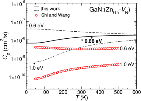
It is important to try and identify the origin of these discrepancies, in order to assess whether they are due to differences in the computational approach and/or differences in the methodology. This type of analysis helps in establishing the validity and reliability of the overall approach and provides important insights. One of the differences between the two calculations is the treatment of the electronic structure of the defect. In our approach all the parameters have been determined consistently using the hybrid functional with =. In Ref. Shi_PRL_2012, most of the results, such as the ground-state geometries, phonon spectra, and electron-phonon coupling matrix elements, were determined using the semilocal PBE functional. The two sets of calculations yield, in particular, very different relaxation energies for the ground state. In our approach, this relaxation energy is 0.67 eV, while the value of 0.43 eV was used in Ref. Shi_PRL_2012, . Unfortunately, we were not able to reproduce this result. Still, to gain insight into the sensitivity to the underlying electronic structure we repeated our calculations using a hybrid functional with a fraction instead of . This yielded eV. The calculated values of decrease by up to a factor of 2, bringing our results in better agreement with Ref. Shi_PRL_2012, .
Another difference between our approach and that of Shi and Wang Shi_PRL_2012 is the inclusion of the scaling factor , discussed in Sec. III.5. In the case of the Zn- complex in GaN, the coupling between the hole state at the point and the defect state is evaluated for a positively charged supercell. If we consider a particle with zero kinetic energy interacting with a repulsive potential, the particle would be repelled to infinity. Therefore the matrix element as well as the product will tend to zero as a function of increasing supercell size [cf. Eqs. (17a), (17b), and (18)]. As a result, performing the calculation of electron-phonon coupling for increasingly larger supercells will not lead to converged results, but rather result in a decreasing value of the coefficient . It is to combat such effects that the scaling factor [Eq. (19)] has been introduced in the first place.Paessler_pssb_1976 ; Bonch-Bruevich_FTT_1959 This effect was not considered in Ref. Shi_PRL_2012, and hence their values obtained for a 300-atom supercell are underestimated. Using the information provided in Ref. Shi_PRL_2012, , we estimate that the values of in Ref. Shi_PRL_2012, are probably too small by a factor of about 1.5. Proper inclusion of the scaling factor would bring the values of Shi and Wang Shi_PRL_2012 closer to ours.
The two sources of discrepancies considered so far still do not account for the fact that our results are more than one order of magnitude larger than those of Shi and Wang.Shi_PRL_2012 One might argue that the consideration of all phonon degrees of freedom in Ref. Shi_PRL_2012, is in principle more accurate than the reduction of the problem to a single effective phonon frequency, as we do in the present work. However, the analysis we will present in Sec. V.2 indicates that one should expect the 1D model to underestimate the true result. This consideration therefore does not resolve the discrepancy either. More careful scrutiny traces the difference between the two approaches to the core assumptions of the method employed in Ref. Shi_PRL_2012, , which was originally proposed by Freed and Jortner.Freed_JCP_1970 The formula of Freed and Jortner is derived from the so-called adiabatic approach within the Condon approximation.Huang_SS_1981 ; Peuker_pssb_1982 This approach has been recognized to underestimate nonradiative capture rates,Huang_SS_1981 ; Peuker_pssb_1982 an issue to be addressed in Sec. V.3.
V Discussion
In this Section we critically analyze our theoretical approach and compare calculated capture coefficients to those in other materials.
V.1 The strength of electron-phonon coupling
In this section we discuss the strength of electron-phonon coupling at defects considered in this work, as expressed by the matrix elements (Table 1). It is informative to estimate the maximum possible value of this matrix element, for typical values of and . According to Eq. (13), we have to find the maximum value of , where is the perturbed valence band and is the defect state. Let us assume that for = (= corresponds to the equilibrium configuration of the ground state) the defect state acquires completely the character of the perturbed valence band, albeit still localized on atoms, with the total number of atoms in the supercell being . We can then use our knowledge about the degree of localization of and , along with the normalization of the wavefunctions, to estimate the matrix element. Replacing the derivative by its finite-difference expression, we see that the maximum value of is . Therefore a large would correspond to as per Eq. (13).
Taking typical values for and from Table 1, assuming that 4, =96, and also that coupling to only one valence band is present, we obtain eV/(amu1/2Å). As shown in Table 1, the actual values for the defects considered here are all within this range. Our estimate of the maximum value of yields important insight: for the defects considered, electron-phonon coupling pertaining to the special mode from Eq. (6) is, in fact, very strong. In the case of hole capture studied in this work, the coupling is very effective for the acceptor defects with electronic states derived from anion 2 orbitals (GaN:C and ZnO:Li), but is also quite significant for the donor defect [GaN:(Zn-)] with electronic states derived mainly from the cation (Ga) 3 states.
V.2 1D vs. multi-dimensional treatment
The nonradiative capture processes studied in this work have been analyzed employing 1D configuration coordinate diagrams. Here, we critically review the range of applicability of this approach.
It is known that different phonons have different functions during a nonradiative transition. Stoneham_RPP_1981 ; Freed_JCP_1970 Vibrational modes that couple the two electronic states very efficiently, i.e., those that yield large electron-phonon matrix elements, are called the “promoting” modes, whereas the modes that couple strongest to the distortion of the geometry during the transition are called the “accepting” modes.Stoneham_RPP_1981 A particular mode can, of course, be both “accepting” and “promoting”.
The 1D treatment of Sec. III.3 essentially considers only the “accepting” modes, reducing the treatment to one effective mode that has the strongest possible “accepting” character, being completely parallel to the distortion of the defect geometry during the transition [Eq. (6)]. For the nonradiative transition to be effective this mode must also have a lot of “promoting” character, i.e., it must couple the two electronic states by producing a sizable electron-phonon matrix element (or ). One therefore expects the calculated transition rate in the 1D treatment to be somewhat smaller than the real one; i.e., the 1D approximation should provide a lower bound.
As we have shown in Sec. V.1, for all the defects studied in this work the “accepting” mode is characterized by a large electron-phonon matrix element, and therefore has a lot of “promoting” character. This justifies the use of the 1D approach for such defects. Still, it should be acknowledged that our calculated capture coefficients might be slightly underestimated. In order to include all phonon modes in a rigorous theoretical treatment, an efficient algorithm to calculate electron-phonon coupling matrix elements for hybrid functionals is urgently needed. While the method used in the present work [cf. Eq. (13) and Fig. 2] is one algorithm to determine those elements, it is computationally too demanding if all phonons need to be included.
V.3 Static and adiabatic formulation of nonradiative transitions
The first-principles methodology presented in this work is based on the static-coupling approach.Paessler_pssb_1975 ; Paessler_CJP_1982 ; Goguenheim_JAP_1990 In Sec. III.2 we stated that this approach is applicable when carrier capture rates are much smaller than phonon lifetimes and periods of lattice vibrations.Paessler_pssb_1975 Now we are in a position to verify this assumption. Note that as per Eq. (1), carrier capture rate can mean two separate things. For a given hole its capture time by any acceptor of the type is (measured in s). However, for a given acceptor in its negative charge state the time it takes to capture a hole is . It is the latter quantity that is of importance when determining the range of validity of the static approach.
For GaN:C and ZnO:Li we compared calculated values to experimental results summarized in Ref. Reshchikov_AIP_2014, . In these experiments typical hole densities were cm-3.Reshchikov_JAP_2005 Using the calculated values for (cf. Figs. 5, 7, 9), we estimate hole capture times s. These values are much larger than typical periods of lattice vibrations s (0.1 ps), or phonon lifetimes, which are at most a few ps. Matulionis_APL_2009 Thus, the transition between the two electronic states [process (1) in Fig. 1 (b)] is indeed the time-limiting step in carrier capture. This transition is a rare event; once it happens, the emission of phonons due to phonon-phonon interaction [process (2) in Fig. 1] occurs almost instantaneously. The range of validity of the static approach can be judged for different defects separately. For example, in the case of hole capture by GaN:C at room temperature, we estimate that the static approach is valid for hole densities up to cm-3.
In parallel with the static approach, which we advocate and justified above, a lot of theoretical work on nonradiative carrier capture employed the so-called adiabatic coupling scheme.Huang_PRCL_1950 ; Freed_JCP_1970 In this approach one chooses Born-Oppenheimer wavefunctions as a starting point for perturbation theory. This choice should be contrasted to the choice made in the static approach, namely , where is a specific fixed atomic configuration (see Sec. III.2). Many early formulations based on the adiabatic approach also assumed that electron-phonon matrix elements were independent of ,Huang_PRCL_1950 ; Freed_JCP_1970 which is the Condon approximation for nonradiative transitions. However, already in the 1970s it was noticed that the adiabatic approach within the Condon approximation yielded capture rates significantly smaller than the static approach applied to the same system.Paessler_pssb_1975 This result was very surprising at the time; indeed, it was expected that far from the intersection of potential energy surfaces the two descriptions should yield very similar physics.
The issue was resolved in the early 1980s by Huang, Huang_SS_1981 Gutsche and co-workers, Gutsche_pssb_1982 ; Peuker_pssb_1982 and Burt.Burt_JPC_1983 The discrepancy was found to originate in an inconsistent application of the adiabatic approach. These authors demonstrated that within the leading order the adiabatic approach does give the same answer as the static approach, provided the adiabatic approach is applied consistently. This can be achieved in one of two ways: (i) by going beyond the Condon approximation in the adiabatic treatment Huang_SS_1981 ; or (ii) by considering all non-diagonal terms in the Hamiltonian.Peuker_pssb_1982 In particular, erroneous omission of non-diagonal terms can lead to significantly smaller values of capture rates in the adiabatic approach.Peuker_pssb_1982 This was exactly the problem of prior theoretical treatments that were based on the adiabatic approach together with the Condon approximation.Huang_PRCL_1950 ; Freed_JCP_1970
The discussion up to this point applies to the case where nonradiative transitions occur far from the intersection of two potential energy surfaces. However, when transitions close to the crossing point are important (as is the case for ZnO:LiZn and GaN:CN, cf. Figs. 6 and 8) the adiabatic approach within the Condon approximation fails altogether. In the adiabatic approach, an avoided crossing occurs between the two potential energy surfaces, leading to a strong variation of electronic wavefunctions and making potential energy surfaces very anharmonic. In such a situation, adiabatic wavefunctions are probably not a good starting point for perturbation theory.Paessler_pssb_1975 The static coupling scheme, on the other hand, is still applicable in the regime close to the intersection of the potential energy surfaces.Paessler_pssb_1975 ; Paessler_CJP_1982
In our opinion, the application of the adiabatic coupling scheme in Ref. Shi_PRL_2012, , versus the static scheme employed in the present work, is the major reason for the differences between our results and those of Ref. Shi_PRL_2012, (Fig. 9). The results of Ref. Shi_PRL_2012, were obtained based on the formula of Freed and Jortner, Freed_JCP_1970 which uses the adiabatic coupling scheme within the Condon approximation and will thus tend to underestimate the values for capture coefficients. Huang_SS_1981 ; Gutsche_pssb_1982 ; Peuker_pssb_1982 ; Burt_JPC_1983
The theoretical foundations of nonradiative capture due to multi-phonon emission were laid in Refs. Huang_PRCL_1950, ; Kubo_PTP_1955, ; Gummel_AP_1957, ; Henry_PRB_1977, ; Freed_JCP_1970, ; Paessler_pssb_1975, ; Huang_SS_1981, ; Gutsche_pssb_1982, ; Peuker_pssb_1982, ; Burt_JPC_1983, ; Paessler_CJP_1982, ; Goguenheim_JAP_1990, . References Huang_SS_1981, ; Gutsche_pssb_1982, ; Peuker_pssb_1982, ; Burt_JPC_1983, , in particular, contain important lessons about the proper application of various approaches. Unfortunately, activity in this field stagnated, partly due to the difficulty of obtaining sufficiently accurate results with the computational methods that were available at the time. The current power of accurate electronic structure methods creates a fertile environment in which to achieve the goal of a quantitative determination of carrier capture rates completely from first principles.
This analysis, which finds its roots in similar discussions of 1970s and 1980s, relates to the underlying theory to describe nonradiative capture and does not undermine the achievements of Ref. Shi_PRL_2012, . Most importantly, in Ref. Shi_PRL_2012, a new efficient algorithm to calculate electron-phonon coupling was proposed. The algorithm considers all phonon degrees of freedom and can be in principle used also in conjunction with the static approach used in the current work. A further extension of the algorithm to hybrid functionals is currently highly desirable.
V.4 Comparison with other materials
It is instructive to compare our results of capture coefficients to those in other materials. However, one should keep in mind that for any given defect the resulting capture rate depends on many parameters, including: (i) details of the cc diagram, for example “classical” barriers for nonradiative capture (cf. Figs. 3, 6, 8); (ii) the strength of electron-phonon coupling [Eqs. (4) and (22)]; (iii) the charge state of the defect [cf. Eqs. (14) and (21)]; (iv) temperature. Furthermore, many experimental papers report capture cross sections rather than capture coefficients . As discussed in Sec. II, the two are related via , where is a characteristic carrier velocity. In the case of non-degenerate carrier statistics the characteristic velocity is the average thermal velocity , which introduces an additional temperature-dependent prefactor in the expression for . These considerations indicate that the comparison of carrier capture characteristics of different defects in different materials should be approached with caution. However, some conclusions can still be drawn.
Let us consider a specific material, and look at carrier capture cross sections for a wide range of defects. Those cross sections will depend on the specific defect, as well as on temperature. However, one could argue that the maximum value of capture cross section across all defects and across all temperature ranges (say, for temperatures where non-degenerate carrier statistics apply), would be indicative of the strength of electron-phonon coupling in the host material.
In their seminal paper, Henry and Lang studied capture cross sections at defects in GaP and GaAs. Henry_PRB_1977 The measurements were performed by deep-level transient spectroscopy over the temperature range 100-600 K, comparable to the temperature range discussed in the present work. Both electron and hole capture was studied. Capture cross sections at various defects ranged from to about Å2 for these temperatures. One could cautiously conclude that Å2 is the maximum capture cross section for any defect system in GaP and GaAs.
For the three defects studied in the present work, calculated hole capture cross sections vary from 0.1 to 200 Å2 in GaN (Figs. 5 and 9), and from 1000 to 2000 Å2 in ZnO (Fig. 7) for a similar temperature range. In particular, we find Å2 in GaN:C at = K, and Å2 for ZnO:Li at K. As discussed in Sec. IV, these results are in agreement with the experimental data of Ref. Reshchikov_AIP_2014, . While our data set is limited, it is clear that carrier capture cross sections in ZnO and GaN tend to be larger than those in GaP and GaAs. We attribute this to the larger strength of electron-phonon interactions in wide-band-gap materials such as GaN and ZnO, compared to GaP and GaAs. This strength directly affects the matrix elements, as discussed in Sec. V.1.
These trends for nonradiative capture at defects are in accord with the knowledge of electron-phonon interactions in bulk solids. Let us take the interaction of free carriers with longitudinal optical (LO) phonons as an example. This strength of this interaction can be characterized by a dimensionless factor, the Fröhlich parameter (in SI units).Ridley For holes, in GaAs and in GaP, while is about 1.0 in GaN and 1.5 in ZnO, indeed indicative of stronger interaction.
VI Conclusions
In conclusion, we have developed a first-principles methodology to study nonradiative carrier capture by means of multiphonon emission at defects in semiconductors. All the parameters, including the electron-phonon coupling, have been determined consistently using hybrid density functional calculations, which yield accurate bulk band structures as well as defect properties. Significant simplifications occur due to the implementation of a 1D model, for which we provided extensive justification, and which also yields useful insights into the defect physics. We applied our methodology to several hole-capturing centers in GaN and ZnO. The resulting capture coefficients are large, and in agreement with experimental data. We conclude that state-of-the-art electronic structure techniques, when combined with reliable methodological approaches, are capable of accurately describing carrier capture processes. The methodology thus allows generating reliable information for defects for which experimental information is incomplete—which seems to be the case for the majority of defects that are potentially relevant for charge trapping or SRH recombination in semiconductor devices. The combination of a first-principles approach with experiment can also be a powerful aid in the identification of defects. Finally, our first-principles approach allows making predictions for new materials for which no experimental data is as yet available.
Acknowledgements
We acknowledge M. A. Reshchikov for valuable interactions and providing us with a preprint of Ref. Reshchikov_AIP_2014, . We also thank L. Shi and L.-W. Wang for sharing their data for GaN:(Zn), A. Carvalho for providing the Li pseudopotential, and C. E. Dreyer, F. Giustino, A. Janotti, J. L. Lyons, J. S. Speck, S. Keller, and C. Weisbuch for fruitful discussions. A.A. was supported by the Office of Science of of the U.S. Department of Energy (Grant No. DE-SC0010689), and by the Swiss NSF (PA00P2134127) during the initial phase of the project. Q.Y. was supported by the UCSB Solid State Lighting and Energy Center. Computational resources were provided by the National Energy Research Scientific Computing Center, which is supported by the DOE Office of Science under Contract No. DE-AC02-05CH11231, and by the Extreme Science and Engineering Discovery Environment (XSEDE), supported by NSF (OCI-1053575 and NSF DMR07-0072N).
References
- (1) U. K. Mishra, P. Parikh, and Y.-F. Wu, Proc. IEEE 90, 1022 (2002).
- (2) V. N. Abakumov, V. I. Perel’, and I. N. Yassievich, Nonradiative Recombinations in Semiconductors (North-Holland, Amsterdam, 1991).
- (3) B. Di Bartolo (ed.), Advances in Nonradiative Processes in Solids (Plenum Press, New York, 1991).
- (4) C. H. Henry and D. V. Lang, Phys. Rev. B 15, 989 (1977).
- (5) K. Huang and A. Rhys, Proc. Royal Soc. 204, 406 (1950).
- (6) R. Kubo and I. Toyozawa, Prog. Theor. Phys. 13, 160 (1955).
- (7) H. Gummel and M. Lax, Annals of Phys. 2, 28 (1957).
- (8) K. F. Freed and J. Jortner, J. Chem. Phys. 52, 6272 (1970).
- (9) R. Pässler, Phys. Status Solidi (b) 68, 69 (1975).
- (10) K. Huang, Scientia Sinica 14, 27 (1981).
- (11) E. Gutsche, Phys. Status Solidi 109, 583 (1982).
- (12) K. Peuker, R. Enderlein, A. Schenk, and E. Gutsche, Phys. Status Solidi 109, 599 (1982).
- (13) M. G. Burt, J. Phys. C: Solid State Phys. 16, 4137 (1983).
- (14) R. Pässler, Czech. J. Phys. 32, 846 (1982).
- (15) D. Goguenheim and M. Lannoo, J. Appl. Phys. 68, 1059 (1990).
- (16) A. M. Stoneham, Theory of Defects in Solids (Oxford University Press, 1975).
- (17) W. H. Strehlow and E. L. Cook, J. Phys. Chem. Ref. Data 2, 163 (1973).
- (18) C. Freysoldt, B. Grabowski, T. Hickel, J. Neugebauer, G. Kresse, A. Janotti, and C. G. Van de Walle, Rev. Mod. Phys. 86, 253 (2014).
- (19) Theory of Defects in Semiconductors, edited by D. A. Drabold and S. Estreicher (Springer, 2007).
- (20) Advanced Calculations for Defects in Materials, edited by A. Alkauskas, P. Deák, J. Neugebauer, A. Pasquarello, and C. G. Van de Walle (Wiley, Weinheim, 2011).
- (21) F. Schanovsky, W. Gös, and T. Grasser, J. Vac. Sci. Technol. B 29, 01A201 (2011).
- (22) F. Schanovsky, O. Baumgartner, V. Sverdlov, and T. Grasser, J. Comput. Electron. 11, 218 (2012).
- (23) K. P. McKenna and J. Blumberger, Phys. Rev. B 86, 245110 (2012).
- (24) R. A. Marcus, Rev. Mod. Phys. 65, 599 (1993).
- (25) L. Shi and L.-W. Wang, Phys. Rev. Lett. 109, 245501 (2012).
- (26) M. A. Reshchikov, A. A. Kvasov, M. F. Bishop, T. McMullen, A. Usikov, V. Soukhoveev, and V. A. Dmitriev, Phys. Rev. B 84, 075212 (2011).
- (27) S. Baroni, S. de Gironcoli, and A. Dal Corso, Rev. Mod. Phys. 73, 515 (2001).
- (28) F. Giustino, M. L. Cohen, and S. G. Louie, Phys. Rev. B 76, 165108 (2007).
- (29) R. Borrelli and A. Peluso, J. Chem. Phys. 119, 8437 (2003).
- (30) N. Nepal, J. Li, M. L. Nakarmi, J. Y. Lin, and H. X. Jiang, Appl. Phys. Lett. 87, 242104 (2005).
- (31) D. C. Reynolds, D. C. Look, B. Jogai, C. W. Litton, G. Cantwell, and W. C. Harsch, Phys. Rev. B 60, 2340 (1999)
- (32) M. A. Reshchikov and H. Morkoç, J. Appl. Phys. 97, 061301 (2005).
- (33) M. A. Reshchikov, H. Morkoç, B. Nemeth, J. Nause, J. Xie, B. Hertog, and A. Osinsky, Physica B 401-402, 358 (2007).
- (34) M. A. Reshchikov, J. Garbus, G. Lopez, M. Ruchala, B. Nemeth, and J. Nause, Mater. Res. Soc. Symp. Proc. 957, 0957-K07-19 (2007).
- (35) M. A. Reshchikov, AIP Conf. Proc. 1583, 127 (2014).
- (36) T. Ogino and M. Aoki, Jap. J. Appl. Phys. 19, 2395 (1980).
- (37) B. K. Meyer, H. Alves, D. M. Hofmann, W. Kriegsies, D. Forster, F. Bertram, J. Christen, A. Hoffmann, M. Strassburg, M. Dworzak, U. Haboeck, and A. V. Rodina, Phys. Status Solidi B 241, 231 (2004)
- (38) J. L. Lyons, A. Janotti, and C. G. Van de Walle, Appl. Phys. Lett. 97, 1521088 (2009).
- (39) A. Matulionis, J. Liberis, I. Matulionienė, M. Ramonas, E. Šermukšnis, J. H. Leach, M. Wu, X. Ni, X. Li, and H. Morkoç, Appl. Phys. Lett. 95, 192102 (2009).
- (40) J. Heyd, G. E. Scuseria, and M. Ernzerhof, J. Chem. Phys. 118, 8207 (2003); ibid. 124, 219906 (2006).
- (41) G. Pacchioni, F. Frigoli, D. Ricci, and J. A. Weil, Phys. Rev. B 63, 054102 (2000).
- (42) P. Deák, A. Gali, A. Solyom, A. Buruzs, and Th. Frauenheim, J. Phys.: Condens. Mat. 17, S2141 (2005).
- (43) A. Alkauskas, P. Broqvist, and A. Pasquarello, Phys. Rev. Lett. 101, 046405 (2008); Phys. Status Solidi B 248, 775 (2011).
- (44) J. L. Lyons, A. Janotti, and C. G. Van de Walle, Phys. Rev. Lett. 108, 156403 (2012).
- (45) J. L. Lyons, A. Janotti, and C. G. Van de Walle, Jap. J. Appl. Phys. 52, 08JJ04 (2013).
- (46) J. P. Perdew, K. Burke, and M. Ernzerhof, Phys. Rev. Lett. 77, 3865 (1996).
- (47) P. E. Blöchl, Phys. Rev. B 50, 17953 (1994).
- (48) G. Kresse and J. Furthmüller, Phys. Rev. B 54, 11169 (1996); G. Kresse and D. Joubert, Phys. Rev. B 59, 1758 (1999).
- (49) J. Paier, M. Marsman, K. Hummer, G. Kresse, I. C. Gerber, amd J. G. Ángyán, J. Chem. Phys. 124, 154709 (2006).
- (50) Semiconductors: Basic Data, 2nd ed., edited by O. Madelung (Springer, Berlin, 1996).
- (51) C. Freysoldt, J. Neugebauer, and C. G. Van de Walle, Phys. Rev. Lett. 102, 016402 (2009); Phys. Status Sol. B 248, 1067 (2011).
- (52) A. Baldereschi, Phys. Rev. B 7, 5212 (1973).
- (53) J. Ihm, A. Zunger, and M.-L. Cohen, J. Phys. C: Solid State Phys. 12, 4409 (1979).
- (54) N. Troullier and J. L. Martins, Phys. Rev. B 43, 1993 (1991).
- (55) M. Fuchs and M. Scheffler, Comput. Phys. Commun. 119, 67 (1999).
- (56) CPMD, Copyright IBM Corp 1990-2006, Copyright MPI für Festkörperforschung Stuttgart 1997-2001; J. Hutter and A. Curioni, ChemPhysChem 6, 1788 (2005).
- (57) T. Todorova, A. P. Seitsonen, J. Hutter, I. F. W. Kuo, and C. J. Mundy, J. Phys. Chem. B 110, 3685 (2006).
- (58) P. Broqvist, A. Alkauskas, and A. Pasquarello, Phys. Rev. B 80, 085114 (2009).
- (59) H.-P. Komsa, P. Broqvist, and A. Pasquarello, Phys. Rev. B 81, 205118 (2010).
- (60) A. Alkauskas, P. Broqvist, F. Devynck, and A. Pasquarello, Phys. Rev. Lett. 101, 106802 (2008).
- (61) X. Wu, E. J. Walter, A. M. Rappe, R. Car, and A. Selloni, Phys. Rev. B 80, 115201 (2009).
- (62) L. Hedin and S. Lundqvist, in Solid State Physics (Ed. F. Seitz, D. Turnbull and H. Ehrenreich), Vol. 23, 1 (1970)
- (63) M.-H. Du and S.-B. Zhang, Phys. Rev. B 80, 115217 (2009).
- (64) A. Carvalho, A. Alkauskas, A. Pasquarello, A. K. Tagantsev, and N. Setter, Phys. Rev. B 80, 195205 (2009).
- (65) T. S. Bjørheim, S. Erdal, K. M. Johansen, K. E. Knutsen, and T. Norby, J. Phys. Chem. C 116, 23764 (2012).
- (66) J. L. Lyons, A. Janotti, and C. G. Van de Walle, in preparation (2014).
- (67) A. Alkauskas, J. L. Lyons, D. Steiauf, and C. G. Van de Walle, Phys. Rev. Lett. 109, 267401 (2012).
- (68) V. L. Bonch-Bruevich, Fiz. Tverd. Tella, Sbornik II, 182 (1959).
- (69) R. Pässler, Phys. Status Solidi B 78, 625 (1976).
- (70) W. Kohn, Phys. Rev. 105, 509 (1957).
- (71) L. D. Landau and L. M. Lifshitz, Quantum Mechanics. Non-relativistic theory (Butterworth-Heinemann, 1981).
- (72) J. J. Pankove, S. Bloom, and G. Harbecke, RCA Rev. 36, 163 (1975).
- (73) B. Šantić, Semicond. Sci. Technology 18, 219 (2003)
- (74) K. Hümmer, Phys. Status Solidi (b) 56, 249 (1973).
- (75) I. Vurgaftman and J. R. Meyer, chapter 2 in Nitride Semiconductor Devices, Ed. J. Piprek, (Wiley-VCH, 2007).
- (76) Q. Yan, P. Rinke, M. Winkelnkemper, A. Qteish, D. Bimberg, M. Scheffler, and C. G. Van de Walle, Semicond. Sci. Technol. 26, 014307 (2011).
- (77) D. O. Demchenko, I. C. Diallo, and M. A. Reshchikov, Phys. Rev. Lett. 110, 087404 (2013).
- (78) C. H. Seager, D. R. Tallant, J. Yu, and W. Götz, J. of Lumin. 106, 115 (2004).
- (79) J. L. Lyons, A. Janotti, and C. G. Van de Walle, Appl. Phys. Lett. 97, 152108 (2010).
- (80) M. A. Reshchikov, in Photoluminescence: Applications, Types and Efficacy, Ed. M. A. Case and B. C. Stout (Nova Science, New York, 2012).
- (81) J. L. Lyons, A. Janotti, and C. G. Van de Walle, Phys. Rev. B 89, 035204 (2014).
- (82) W. Chen and A. Pasquarello, Phys. Rev. B 88, 115104 (2013).
- (83) S. Lany and A. Zunger, Phys. Rev. B 80, 085202 (2009).
- (84) A. M. Stoneham, Rep. Prog. Phys. 44, 1251 (1981).
- (85) See, e.g., p. 62 of B. K. Ridley, Quantum Processes in Semiconductors (Clarendon Press, 1999).