Robust recipe for low-resistance ohmic contacts to a two-dimensional electron gas in a GaAs/AlGaAs heterostructure
Abstract
The study of electron transport in low-dimensional systems is of importance, not only from a fundamental point of view, but also for future electronic and spintronic devices. In this context heterostructures containing a two-dimensional electron gas (2DEG) are a key technology. In particular GaAs/AlGaAs heterostructures, with a 2DEG at typically 100 nm below the surface, are widely studied. In order to explore electron transport in such systems, low-resistance ohmic contacts are required that connect the 2DEG to macroscopic measurement leads at the surface. Here we report on designing and measuring a dedicated device for unraveling the various resistance contributions in such contacts, which include pristine 2DEG series resistance, the 2DEG resistance under a contact, the contact resistance itself, and the influence of pressing a bonding wire onto a contact. We also report here a robust recipe for contacts with very low resistance, with values that do not change significantly for annealing times between 20 and 350 sec, hence providing the flexibility to use this method for materials with different 2DEG depths. The type of heating used for annealing is found to strongly influence the annealing process and hence the quality of the resulting contacts.
Keywords: III-V semiconductors, Ohmic contacts, heterostructures, 2DEG, Electrical properties
1 Introduction
The two-dimensional electron gas (2DEG) is of interest for the study of low-dimensional systems, and high-mobility 2DEGs can be realized in epitaxially grown GaAs/ heterostructures 9Beenakker1991 ; 9Kouwenhoven1998 . For performing electrical transport experiments on these systems ohmic contacts to the 2DEG are very important, and these can be realized by annealing samples after a metal alloy has been deposited on the surface at the intended contact areas. Commonly, an alloy consisting of AuGe/Ni/Au is used 9Baca1997 . The annealing times and temperatures that give the lowest contact-resistance values are different for different 2DEG depths. In our previous work IqbalSST2013 ; PhDThesis we optimized such a recipe for annealing in a glass-tube oven. For the study presented here, we used different annealing conditions, namely annealing in a Rapid Thermal Annealer (RTA). Surprisingly, annealing with the RTA gives much lower contact-resistance values with similar values for a very wide range of annealing times. These results are attributed to the exact heating profile as a function of time during annealing, and the process that we followed for cleaning the samples. We already applied our recipes for ohmic contacts in our studies of quantum point contacts in a 2DEG IqbalNat2013 ; IqbalJAP2013 .
The AuGe/Ni/Au material was first used by Braslau et al. 9Braslau1967 to make an ohmic contact to n-GaAs in 1967. Subsequent studies aimed at improving such contacts and understanding the annealing mechanisms 9Ogawa1980 ; 9Braslau1981 ; 9Lee1981 ; 9Heiblum1982 ; 9Kuan1983 ; 9Braslau1983 ; 9Braslau1986 ; 9Procop1987 ; 9Waldrop1987 ; 9Bruce1987 ; 9Shappirio1987 ; 9Relling1988 ; 9Weizer1988 ; 9Lumpkin1996 . Later on, with the increasing importance of the 2DEG in a GaAs/ heterostructure, research focussed on making ohmic contacts to the buried 2DEG 9Zwicknagl1986 ; 9Higman1986 ; 9Rai1988 ; 9Jin1991 ; 9Taylor1994 ; 9Messica1995 ; 9Taylor1998 ; 9Raiser2005 ; 9Saravanan2008 . Despite these extensive studies, a model was missing that could predict the optimal annealing times and temperatures for different depths of the 2DEG. In our previous work we developed such a model IqbalSST2013 ; PhDThesis . In order to understand the annealing mechanism further, we studied the contact-resistance values as a function of circumference and area of the ohmic contacts. However, no clear dependence on circumference or area was found IqbalSST2013 ; PhDThesis , in part because of lack of information on whether the 2DEG square resistance under an ohmic contact changes during the annealing with respect to the square resistance of pristine 2DEG. In addition, it was unknown whether pressing a bonding wire on a contact influences the resistance, as it can possibly rapture the ohmic contact layer over a significant area. Here we report on studying these questions. We designed a dedicated device structure that allowed us to study the contact resistance with various resistance contributions in more detail, and with different measurement methods (3-point measurement, 4-point measurement and the Transmission Line Method (TLM) 8Berger1972TLM ; 8Reeves1982TLM ).
All the results presented in this paper are from samples annealed in a rapid thermal annealer (RTA), unlike our previous work where the hot gas flow in a glass-tube furnace was used for annealing the samples. In the present study we focused on changes in the mentioned contact resistance contributions as a function of annealing time (at fixed annealing temperature and depth of the 2DEG). However, the contact resistance values that we found were, for all samples, so low that we could not obtain sufficient measurement accuracy for determining a dependence on annealing time for the square resistance of 2DEG under an ohmic contact. Instead, the value of these results is that we found a very robust recipe for low contact-resistance values, with values that do not change significantly for annealing times between 20 and 350 sec. This kind of robust recipe is useful for annealing contacts on 2DEG materials with different 2DEG depths where one would need a large margin for suitable annealing times. Our results also show that the details of how the sample is heated have a strong influence on the annealing mechanism.
2 Experimental details
For the present study we used two different wafers, one with the 2DEG at 60 nm depth (wafer I, purchased from Sumitomo Electric Industries, Inc.) and one with the 2DEG at 180 nm depth (wafer II, grown by our team in Bochum). Unless mentioned otherwise, we present results of devices that were fabricated with wafer I. The study of devices from wafer II were less extensive but we will mention the results that are relevant. All the measurements were performed in a liquid helium vessel at 4.2 K.
Wafer I was a GaAs/ heterostructure. The layer sequence of the heterostructure was as follows (top to bottom): a 5 nm -GaAs cap, 40 nm -doped with Si at , a 15 nm nominally intrinsic spacer layer, and a 800 nm GaAs layer. The 2DEG is located at the interface of the AlGaAs spacer layer and the next GaAs layer. The 2DEG density and mobility at K were and , respectively. Wafer II was a similar GaAs/ heterostructure with the layer sequence (top to bottom): a 5 nm -GaAs cap, 70 nm , 70 nm -doped with Si at , 35 nm , and 650 nm GaAs. It had and .
Several cleaning steps during ohmic contact fabrication are very important for getting low-resistance ohmic contacts. The cleaning process is done before starting the ohmic contact fabrication. The samples are first cleaned in acetone, and then in iso-propyl-alcohol, while keeping the sample in an ultrasonic bath on a low power. The samples are then visually inspected and only samples that appear fully clean are used. We observed that contaminated samples show high resistance values and results that cannot be reproduced.
The size of the ohmic contacts was 200 by 200 and they were patterned with electron-beam lithography. For the ohmic contacts, layers of AuGe in eutectic-composition (12 wt Ge, 150 nm), Ni (30 nm) and Au (20 nm) were deposited subsequently by electron-beam evaporation. The contacts were annealed at 450 ∘C in the rapid thermal annealer (RTA, model Jipelec Jet 150) for various times. Annealing took place in a clean flow (600 sccm) to avoid oxidation and material vapors adhering back onto the sample. During annealing the functional sample surface was directly facing the RTA heating lamps.
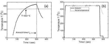
The annealing temperature profiles for the glass-tube oven (used in our previous work IqbalSST2013 ) and the RTA are shown in Fig. 1a,b. For the glass-tube oven, the sample is brought into a pre-heated oven and the temperature rise of the sample holder to the AuGe-eutectic temperature (363∘C) takes a few minutes (not easily controllable). For the RTA, on the other hand, the temperature ramp rate can be controlled and the time for reaching the set temperature was set at the much shorter (but for RTA heating typical) value of 5 sec. This is started with the sample already in the oven. The black and light gray lines in Fig. 1b are for the set temperature and the actual temperature as measured by the thermocouple attached to the surface where sample is placed for annealing. All the results presented in this paper are for samples annealed in the RTA.
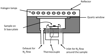
Fig. 2 shows a schematic of the RTA annealing chamber. The heating sources are the halogen lamps that transmit radiation through a quartz window above the sample surface. The sample is placed on a Si base plate and a thermocouple is attached to this plate for measuring the annealing temperature during the process. The flow of gas is maintained during the entire annealing process and cool down.
3 Device design, measurement schemes and methods
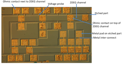
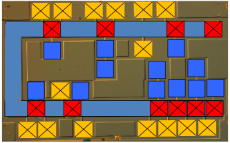
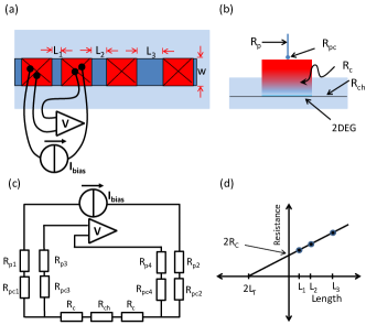
We designed a dedicated device structure for being able to study the different contact-resistance contributions with different measurement methods. An optical image of a fabricated device is shown in Fig. 3. A 200 wide 2DEG channel is defined (U-shaped) by wet etching such that a homogeneous current flow can be applied through the defined strip. Different parts of the devices are labeled. The ohmic contacts are realized on top of the channel as well as on the sides of the channel. The available distances (defined as in Fig. 5a) between the contacts on top of the channel are 40, 260, 460, 660, and 860 . The effect of annealing times on the pristine 2DEG square resistance, and on the full contact resistance and 2DEG square resistance under ohmic contacts are determined using the ohmic contacts deposited on top of the 2DEG channel. The ohmic contacts deposited on the sides are connected to the 2DEG channel via narrow 2DEG strips (20 wide) and serve as voltage probes (used when measuring the resistance of the contacts, the resistance of pristine 2DEG and the resistance of 2DEG under contacts). Metal pads and metal inter-connects between pads are deposited on etched parts of the device. These metal pads are connected to the ohmic contacts via metal inter-connects and used for measuring the ohmic contact resistances without directly bonding on the ohmic contacts themselves (the resistance contributions from metal pads and inter-connects are subtracted in this case). By comparing values measured with this bonding scheme to a subsequent measurement with bonding directly on top of the ohmic contacts, the influence of pressing a bonding wire on an ohmic contact can be determined. The color scheme in Fig. 4 further illustrates the various device parts more clearly. The long 2DEG channel is shown with a light blue color. The ohmic contacts are shown as crossed color squares, with contacts on top of the 2DEG channel in red and side contacts in yellow. The metal pads on etched regions are shown as dark blue squares.
Fig. 5 and Fig. 6 show the various measurement schemes that we applied in this study. We first explain the Transmission Line Method (TLM) before explaining the other measurement schemes. The TLM method 8Berger1972TLM ; 8Reeves1982TLM is a very accurate method for measuring the values of pristine 2DEG square resistance and ohmic-contact resistance, and is widely used in research on ohmic contacts. Fig. 5 shows how the TLM method works. The contacts are made on a 2DEG strip with an increasing distance between pairs of adjacent contacts (Fig. 5a). The width of the contact and channel is labeled as . For resistance measurements a four point current-biased scheme is used (Fig. 5a). This measurement is carried out for all the consecutive contact pairs. Fig. 5b shows a schematic of a side view on one of the contacts and the resistance contributions that play a role. The resistance contributions are (probe resistance), (probe-to-contact resistance), (actual contact resistance between metal pad on the surface and 2DEG) and (2DEG resistance of the channel between the contacts). Fig. 5c shows the corresponding circuit diagram for the complete four-probe scheme. Since the probe () and the probe-to-contact resistances () are negligible as compared to the input resistance of the voltmeter they can be neglected. The total resistance measured between pairs of consecutive contacts is then
| (1) |
The plot in Fig. 5d illustrates how to extract the contact and 2DEG square resistance values from the TLM data. The values are plotted as a function of the channel length. The resistance contribution increases linearly with increasing channel length and shows a linear dependence with an offset from zero that is equal to . A linear fit to the data points can thus be used to obtain . In addition, the slope of the provides an accurate measure for the square resistance of pristine 2DEG (2DEG between contacts). Using that this can be expressed as , where the transfer length is defined using the intercept at zero resistance for the linear trend (see Fig. 5d). Our experiment indeed only gave results with a linear dependence of on for (no significant deviations). While data for is candidate for showing deviations from the linear trend (which can give insight in the resistance distribution inside a contact), this data was discarded for the TLM analysis since it showed large fluctuations (because it is more sensitive to the exact alignment of the contact edges).
We used an extended TLM scheme with first measurements that used bonding on the metal side pads (not shown in Fig. 5) and subsequently measurements that used bonding directly on top of the ohmic contacts (as in Fig. 5) to investigate the influence of pressing a bonding wire on an ohmic contact. Column 6 and 7 in Table 1 show the contact resistance values measured by the TLM method with bonding wires on metal side pads and ohmic contacts respectively. We observe here values that are significantly lower for the case with bonding directly on the ohmic contacts. However, while TLM results give accurate results for , it is not possible to use it for measuring the 2DEG resistance under an ohmic contact. It also does not give information on where inside a contact the contributions to contact resistance arise, while such information is required for detailed understanding of the annealing mechanism, and understanding the differences between the results in column 6 and 7 in Table 1.
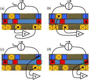
We now discuss other measurement schemes that we applied for determining the various resistance contributions. For a first round of measurements (this order was carried out in parallel with the TLM measurements) bonding wires were pressed on the side ohmic contacts. Two ohmic contacts on top of the 2DEG channel are used for injecting current into the channel (Fig. 6a,b). The voltage drop across a known length of pristine 2DEG channel or 2DEG under an ohmic contacts can then be measured with the voltage probes. The measured values (square resistance of pristine 2DEG, no significant deviations from the TLM values) and (square resistance of 2DEG below an ohmic contact) are shown in column 2 and 3 of the Table 1, respectively.
For a second round of measurements, two bonding wires were pressed onto each metal side pad that connects to the metal layer of an ohmic contact on top of the channel (Fig. 6c). The resistance contributions from the metal side pads and metal inter-connects (measured on each sample, typically 10 ) were measured separately and are subtracted. This measurement scheme directly gives values for the total contact resistance of contacts, which are denoted as and are shown in column 4 of Table 1.
A third round of measurements was carried out as in Fig. 6d. This scheme gives directly a value for the total contact resistance of contacts with the bonding wires pressed directly on top of the contact that is measured. The results are denoted as and are shown in column 5 of Table 1.
All the resistance values measured with various schemes are thus collected in Table 1 for different annealing times. The reported values are average of (in most cases) 5 contacts. The reported error margins for column 2 to 5 are the standard deviations of these results. For column 6 and 7, the standard error values obtained from fitting the linear trend are shown.
4 Results and discussions
| Fig. 6a | Fig. 6b | Fig. 6c | Fig. 6d | Fig. 5 | Fig. 5 | |
| 20 | 19.911.07 | 2.251.18 | 8.600.75 | 4.490.36 | 9.184.5 | 0.413.4 |
| 50 | 19.611.56 | 3.000.30 | 5.291.19 | 4.000.28 | 6.282.86 | 1.241.13 |
| 100 | 19.500.60 | 3.171.55 | 9.040.62 | 4.470.45 | 9.770.80 | 2.380.41 |
| 350 | 20.770.39 | 3.780.38 | 7.761.02 | 4.440.37 | not measured | 2.300.30 |
Table 1 thus lists all the measured resistance values that were introduced. We used in total 4 bonding steps on each device to perform the subsequent measurements (in part because of a limited number of measurement wires in the setup). The order of the measurements was the following: (i) Column 2 and 3; (ii) Column 6; (iii) Column 4; (iv) Column 5 and 7.
The 2DEG resistance under the ohmic contacts is by about a factor 6 lower than the resistance of the pristine 2DEG (columns 2 and 3). This occurs for all annealing times. A previous study on ohmic contacts by G. Sai Saravanan et al. 9Saravanan2008 and our results IqbalSST2013 show that upon annealing Germanium diffuses from the surface towards 2DEG, and this increases -doping near the 2DEG. While this can reduce the mobility in this region, the effective 2DEG square resistance apparently decrease due to the higher doping level. The resistance values are almost constant for all the annealing times that we studied (20 to 350 sec). This suggests that Ge diffuses to 2DEG region already for short annealing times and that the Ge concentration does not change significantly anymore for longer annealing times.
| 20 | 0.413.4 | 0.0820.68 | 1.641.36 | 0.272.26 |
| 50 | 1.241.13 | 0.2480.226 | 4.964.52 | 0.830.75 |
| 100 | 2.380.41 | 0.4760.82 | 9.521.64 | 1.590.27 |
| 350 | 2.300.30 | 0.460.06 | 9.21.2 | 1.530.2 |
Columns 4 to 7 in Table 1 show the contact resistance values as measured with different measurement schemes. The results show significant differences, that we can partly explain and which provide some insight in the different contributions to the contact resistance. As a starting point of the discussion we use the values in column 7, which is the TLM result for directly bonding on the ohmic contacts. This is the most unambiguous number for the contact resistance. Column 5 lists the contact resistance values measured with the 3-point method with bonding directly on the ohmic contact. Column 5 has values that are typically 3 higher than the values in column 7. This can be explained by the fact that the result of column 5 contains a series resistance contribution from a 30 wide region of pristine 2DEG (from the distance between the ohmic contact and the 2DEG voltage probe, this 2DEG part is encircled in green in Fig. 6d). The expected resistance contribution of this part is indeed (using of column 2). This effect was also used for correcting the values of in column 3.
Column 6 shows resistance values from the TLM method with bonding on the side pad (note that 2 side pads are involved) and these results are about higher than the values in column 7. Similarly, the results of column 4 (3-point, bonding on pad, note that only 1 side pad is involved) are about higher than the values in column 5 (3-point, bonding on ohmic). Here we must consider two possible explanations. The first is that the act of pressing a bond wire on top of the ohmic contact results in a lowering of the effective contact resistance by about . The second possibility is that it results from the fact that the metal side pads are only connected to the surface metal of the ohmic-contact at one narrow point. This can yield that on average the spreading resistance inside the contact gives a contribution that is about higher for the cases with bonding on the side pads. Given that all our measurement results and the various contributions are on the scale of only a few , we can not distinguish these cases (we could rule out that it was due to series resistance inside the metal side pad and its inter-connect).
Our results do not allow for more detailed conclusions on the various contributions to the contact resistance or on the annealing mechanism. The reason is that the measured resistance values were all much lower than expected (given our earlier work IqbalSST2013 ) and that the results showed, surprisingly, almost no dependence on the annealing time. In addition, the possible effects of spreading resistance and small series-resistance contributions are all on the scale of a few , and these values are close to the total contact resistance values and their statistical variation. This rules out that further analysis of our present results can give sufficient accuracy for answering the questions that we aimed to study.
At the same time, it is an interesting result that we find very low contact-resistance values, and that the values do almost not change when changing the annealing time by a factor 18. In addition, these contact resistance values rank among the lowest reported values 9Jin1991 . Table 2 provides different representations of the resistance values that we obtained. These values are useful for a comparison to values in the literature where authors present values of contact resistance in various ways. When comparing the literature one also needs to account for a dependence on the depth of the 2DEG and the thickness of the buffer layer. Our results on the wafer with the 2DEG at 180 nm depth (instead of 60 nm) show indeed slightly higher values, with for . Also these samples showed almost no dependence on annealing time (similar results for 30 sec and 550 sec).
We have at this stage little insight why the fabrication method that we used gives such low contact-resistance values, while also being very robust against a variation in annealing time. We have some initial results that point out that the variation of the heating profile as a function of time during annealing is important. For the experiments on the samples with the 2DEG at 180 nm depth we compared results of annealing for 550 and 600 sec annealing times with 5 sec RTA ramp time, to results for 550 sec annealing time that started after a 120 sec RTA ramp time (similar to the glass-tube oven ). The samples of the latter batch had contact resistance values that were twice as high. A second important difference with our earlier work IqbalSST2013 is that the glass-tube oven heats the sample in a gas flow, while the RTA heats the sample by radiation. This can influence the exact way the surface metallization gets heated, and thereby have an influence on the annealing mechanism. Finally, there is possibly a role for having a suitable very clean flow during annealing, and a very clean sample surface before fabrication is started (samples that appeared dirty upon inspection did not yield results with low contact-resistance values).
We do not speculate which possible microscopic model of the ohmic contact forming could be the most appropriate one. Our present work shows that it is certain that the heterostructure right underneath the metallization is completely degenerated, either homogeneously IqbalSST2013 or in contact spikes 9Taylor1994 ; 9Taylor1998 . In the first case, the contact conductivity should be proportional the the circumference length which we cannot check due to the fixed dimensions in this study. In the latter case of contact spikes it depends on their spacing: If they are closely packed, the circumference should again determine the conductivity. If they are more apart, the area could be the leading term. The transmission-electron-microscope studies of our earlier work IqbalSST2013 did rule out a role for spike formation. However, given the very different behavior of the annealing step we cannot conclude that this also holds for the present study.
5 Conclusions
We developed a dedicated device to study and unravel the various contributions to the resistance values of an ohmic contact. We could show that the 2DEG resistance under an ohmic contact gets lower upon annealing, and that pressing a bonding wire onto an ohmic contact either has little influence or only lowers it by a few . However, we could not fully exploit the measurement possibilities of our device design because we obtained very low contact-resistance values that showed no clear dependence on annealing times when these were varied from 20 to 350 sec. Preliminary measurements show that these results can be obtained with rapid heating (5 sec ramp time) during annealing, and that slower ramp times cause higher contact resistance values. A comparison with our earlier work IqbalSST2013 also suggests that heating by radiation gives lower contact resistance values than heating samples in a hot gas flow.
Acknowledgements.
We thank B. Wolfs, J. Holstein and M. de Roosz for technical assistance. A.D.W. acknowledges financial support from the Research school Ruhr-Universität Bochum and the German programs BMBF Q.com-H 16KIS0109, Mercur Pr-2013-0001, and the DFH/UFA CDFA-05-06. M.J.I. acknowledges a scholarship from the Higher Education Commission of Pakistan.References
- (1) See for example: Beenakker, C. W. J. and van Houten, H. (1991), Solid State Physics, 44, 1-228.
- (2) See for example: Sohn, L. L. , Kouwenhoven, L.P., and Schön, eds., G. (1997), Mesoscopic Electron Transport, NATO ASI Series E, 345 (Kluwer, Dordrecht, Netherlands).
- (3) For a review see: Baca, A. G., Ren, F., Zolper, J. C., Briggs, R. D., and Pearton, S. J. (1997), ”A survey of ohmic contacts to III-V compound semiconductors”, Thin Solid Films 308-309, 599.
- (4) Koop, E. J., Iqbal, M. J., Limbach, F., Boute, M., van Wees, B. J., Reuter, D., Wieck, A. D., Kooi, B. J., and van der Wal, C. H. (2013), ”On the annealing mechanism of AuGe/Ni/Au ohmic contacts to a two-dimensional electron gas in GaAs/AlGaAs heterostructures”, Semicond. Sci. Technol., 28, 025006.
-
(5)
Iqbal, M. J., Ph.D. thesis,
http://irs.ub.rug.nl/ppn/344115682. - (6) Iqbal, M. J., Levy, R., Koop, E. J., Dekker, J. B., De Jong, J. P., van der Velde, J. H. M., Reuter, D., Wieck, A. D., Aguado, R., Meir, Y. and van der Wal, C. H. (2013), ”Odd and even Kondo effects from emergent localization in quantum point contacts”, Nature, 501(7465), 79-83.
- (7) Iqbal, M. J., De. Jong, J. P., Reuter, D., Wieck, A. D. and van der Wal, C. H. (2013), ”Split-gate quantum point contacts with tunable channel length”, J. Appl. Phys., 113(2), 024507(1-7).
- (8) Braslau, N., Gunn, J. B., and Staples, J. L. (1967), ”Metal-semiconductor contacts for GaAs bulk effect devices”, Solid-State Electron., 10(5), 381-383.
- (9) Ogawa, M. (1980), ”Alloying behavior of Ni/Au/Ge films on GaAs”, J. Appl. Phys., 51(1), 406-412.
- (10) Braslau, N. (1981), ”Alloyed ohmic contacts to GaAs”, J. Vac. Sci. Technol., 19(3), 803-807.
- (11) Lee, C. P., Welch, B. M., and Tandon, J. L. (1981),”Reliability of pulsed electron-beam-alloyed AuGe/Pt ohmic contacts on GaAs” Appl. Phys. Lett., 39(7), 556-558.
- (12) Heiblum, M., Nathan, M. I., and Chang, C. A. (1982), ”Characteristics of AuGe/Ni ohmic contacts to GaAs”, Solid-State Electron., 25(3), 185-195.
- (13) Kuan, T. S., Batson, P. E., Jackson, T. N., Rupprecht, H., and Wilkie, E. L. (1983), ”Electron microscope studies of an alloyed Au/Ni/AuGe ohmic contact to GaAs ” J. Appl. Phys., 54(12), 6952-6957.
- (14) Braslau, N. (1983), ”Ohmic contacts to GaAs” Thin Solid Films 104(3-4), 391-397.
- (15) Braslau, N. (1986), ”Contact and metallization problems in GaAs integrated circuits”, J. Vac. Sci. Technol. A, 4(6), 3085-3090.
- (16) Procop, M., Sandow, B., Raidt, H., and Son, L. D. (1987), ”The importance of the Ni to Ge ratio and of the annealing cycle for the resistivity and morphology of Ni/AuGe Ohmic contacts to n-GaAs”, Phys. Stat. Sol. A, 104(2), 903-916.
- (17) Waldrop, J. R. and Grant, R. W. (1987), ”Correlation of interface composition and barrier height for model AuGe/Ni contacts to GaAs”, Appl. Phys. Lett., 50(5), 250-253.
- (18) Bruce, R. A. and Piercy, G. R. (1987), ”An improved Au-Ge-Ni ohmic contact to n-type GaAs”, Solid-State Electron., 30(7), 729-737.
- (19) Shappirio, J. R., Lareau, R. T., Lux, R. A., Finnegan, J. J. , Smith, D. D., Heath, L. S., and Taysing-Lara, M. (1987), ”Metal penetration and dopant redistribution beneath alloyed Ohmic contacts to n-GaAs”, J. Vac. Sci. Technol. A, 5(4), 1503-1507.
- (20) Relling, E. and Botha, A. P. (1988), ”Solid state diffusion in GaAs/AuGe/Ni and GaAs/Ni/AuGe/Ni ohmic contacts”, Appl. Surf. Scie., 35(3), 380-387.
- (21) Weizer, V. G. and Fatemi, N. S. (1988), ”The interaction of gold with gallium arsenide”, J. Appl. Phys., 64(9), 4618-4623.
- (22) Lumpkin, N. E., Lumpkin, G. R., and Butcher, K. S. A. (1996), ”Investigation of low- and high-resistance Ni/GeAu ohmic contacts to GaAs using electron microbeam and surface analytical techniques”, J. Mater. Res., 11(5), 1244-1254.
- (23) Zwicknagl, P., Mukherjee, S. D., Capani, P. M., Lee, H., Griem, H. T., Rathbun, L., Berry, J. D., Jones, W. L., and Eastman, L. F. (1986), ”Very low resistance Au/Ge/Ni/Ag based Ohmic contact formation to and heterostructures: A behavioral comparison”, J. Vac. Sci. Technol. B, 4(2), 476-484.
- (24) Higman, T. K. , Emanuel, M. A., Coleman, J. J., Jeng, S. J., and Wayman, C. M. (1986), ”Structural analysis of Au/Ni/Ge and Au/Ag/Ge alloyed ohmic contacts on modulation-doped AlGaAs/GaAs heterostructures”, J. Appl. Phys., 60(2), 677-680.
- (25) Rai, A. K., Ezis, A., Graham, R. J., Sharma, R., and Langer, D. W. (1988), ”Microstructural characterization of AlGaAs-GaAs modulation-doped field-effect transistor ohmic contacts formed by transient annealing”, J. Appl. Phys., 63(9), 4723-4727.
- (26) Jin, Y. (1991), ”Ohmic contact to n-type bulk and doped MODFET type heterostructures and its applications”, Solid-State Electron., 34(2), 117-121.
- (27) Taylor, R. P., Coleridge, P. T., Davies, M., Feng, Y., McCaffrey, J. P., and Marshall, P. A. (1994), ”Physical and electrical investigation of ohmic contacts to AlGaAs/GaAs heterostructures”, J. Appl. Phys., 76(12), 7966-7972.
- (28) Messica, A., Meirav, U., and Shtrikman, H. (1995), ”Refractory metal-based low-resistance ohmic contacts for submicron GaAs heterostructure devices”, Thin Solid Films, 257(1), 54-57.
- (29) Taylor, R. P., Newbury, R., Sachrajda, A. S., Feng, Y., Coleridge, P. T., Davies, M., and McCaffrey, J. P. (1998), ”Investigation of the current injection properties of ohmic spikes in nanostructures”, Superl. Microstr., 24(5), 337-345.
- (30) Raiser, S., Graumann, U., Fleischer, M., Schmid, J., Jauerneck, S., Weis, J., and Wharam, D. A., Scientific program of the 2005 German DPG meeting, abstract HL 58.67 (unpublished); http://www.dpg-tagungen.de/archive/.
- (31) Sai Saravanan, G., Mahadeva Bhat, K., Muraleedharan, K., Vyas, H. P., Muralidharan, R., and Pathak, A. P. (2008), ”Ohmic contacts to pseudomorphic HEMTs with low contact resistance due to enhanced Ge penetration through AlGaAs layers”, Semicond. Sci. Technol.,23(2), 025019(1-6).
- (32) Berger, H. H. (1972), ”Models for contacts to planar devices”, Solid-State Electron., 15(2), 145-158.
- (33) Reeves, G. K. and Harrison, H. B. (1982), ”Obtaining the specific contact resistance from transmission line model measurements”, IEEE Electron Device Lett., 3(5), 111-113.