Origin of traps and charge transport mechanism in hafnia
Abstract
In this study, we demonstrated experimentally and theoretically that oxygen vacancies are responsible for the charge transport in \ceHfO2. Basing on the model of phonon-assisted tunneling between traps, and assuming that the electron traps are oxygen vacancies, good quantitative agreement between the experimental and theoretical data of current-voltage characteristics were achieved. The thermal trap energy of eV in \ceHfO2 was determined based on the charge transport experiments.
pacs:
77.55.df, 77.84.Bw, 72.20.i, 72.20.JvKnowledge about charge transport mechanisms hafnia (hafnium oxide, \ceHfO2) is crucial for modern microelectronics, because high- \ceHfO2 is used as a gate dielectric in high-speed MOSFETs Ma et al. (2005); Robertson (2006) and FinFETs Pavanello et al. (2007); Tsormpatzoglou et al. (2009) and a blocking insulator in \ceSi-oxide-nitride-oxide-silicon-type (SONOS) flash memory cells Chen et al. (2011); Tsai et al. (2009). Hafnia is a promising candidate to used sa active medium in resistive random access memory, which would involve combining the most favorable properties of both high-speed dynamic random access memory and non-volatile flash memory Yang et al. (2008); Goux et al. (2010); Wang et al. (2012). However, an unresolved physics is the nature of defects and traps that are responsible for the charge transport in \ceHfO2. The atomic structure of defect that affects the localization and charge transport still remains unclear. Currently, the accepted hypothesis is that oxygen vacancies are responsible for charge transport in dielectric. Although many studies have investigated the theory of the atomic and electronic structure of oxygen vacancies in hafnia Guha and Narayanan (2007); Muñoz Ramo et al. (2007a); Foster et al. (2002); Zheng et al. (2007); Muñoz Ramo et al. (2007b); Jiang et al. (2010); Xiong et al. (2005); Broqvist and Pasquarello (2006), direct experimental data regarding the presence of oxygen vacancies in hafnia were reported recently Perevalov et al. (2014). It was shown that oxygen vacancies in hafnia are responsible for blue luminescence band at eV and a luminescence excitation band at eV, and a hypothesis that the oxygen vacancies in hafnia act as traps in charge transport through the dielectric was discussed Perevalov et al. (2014). In this case thermal energy traps in \ceHfO2 is equal to a half of the Stokes luminescence shift eV.
A lot of charge transport studies described experiment results by Pool-Frenkel (PF) mechanism in hafnia-based structures Sahoo and Misra (2011); Pan et al. (2007); Zhu et al. (2002). However, the most investigations explained their results qualitatively, and did not get quantitative agreement of the phenomenological parameters such as dynamic permittivity, trap energy, frequency factor etc. The most part of transport investigations did not get into account neither charge trap density, which depends on thin film fabrication technology, nor phonon influence on electron and hole transport, which might be significant at high temperatures.
In this letter, we phonon-assisted tunneling between traps conduction mechanism in \ceHfO2 was developed with good quantitative as well as qualitative agreement. It was clearly shown that oxygen vacancies are responsible for the charge transport in \ceHfO2 and \ceHfO2-based devices.
Transport measurements were performed for metal-insulator-semiconductor (MIS) and metal-insulator-metal (MIM) structures. For the MIS \ceSi/\ceHfO_x/\ceNi structures, the 20-nm-thick amorphous hafnia was deposited on a -type Si \hkl(100) wafer by using the atomic layer deposition (ALD) system. Tetrakis dimethyl amino hafnium (TDMAHf) and water vapor were used as precursors at a chamber temperature of C for \ceHfO_x film deposition.
Another set of MIS samples with 8-nm-thick \ceHfO_x films was fabricated using physical vapor deposition (PVD). A pure \ceHfO2 target was spattered by an electron beam, and \ceHfO2 were deposited on the -type Si \hkl(100) wafer. Low temperature post-deposition annealing (PDA) during min at C was applied to prevent the growth of interfacial \ceSiO_x Lin et al. (2009). Structural analysis shows that the resulting \ceHfO_x films were amorphous. To fabricate \ceSi/\ceTaN/\ceHfO_x/\ceNi MIM structures, we deposited the 8-nm-thick amorphous hafnia on 100-nm-thick TaN films on \ceSi wafers, using PVD. We did not apply any post-deposition annealing to produce the most non-stoichiometric films. All samples for transport measurements were equipped with round 50-nm-thick Ni gates with a radius of m. Transport measurements were performed using a Hewlett Packard 4155B semiconductor parameter analyzer and an Agilent E4980A precision LCR meter.
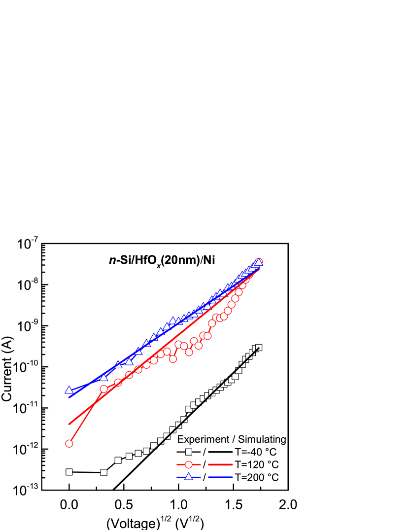
The experimental current-voltage (-) characteristics in MIS(PVD) structures, measured at different temperatures with a positive bias applied to the \ceNi contact, are shown in Fig. 1, graphed by different characters in PF (-) plot. The current grows exponentially with increasing of the gate voltage and temperature. We attempted to explain the experimental data by using isolated trap ionization model:
| (1) |
where is the current density, is the electron charge, is the charge trap density, is the probability of trap ionization per second, and has different dependencies on electric field and temperature. In term of PF model the probability is
| (2) |
is the frequency factor which was defined as , is thermal trap energy (the energy of thermal ionization of the trap), is the Planck constant, is Poole–Frenkel coefficient, is the electric field, and is the Boltzmann constant Frenkel (1938). Experimental - characteristics and results of the fitting procedure are shown in Fig. 1. As can be seen, Frenkel model (2) describes the experiment data qualitatively very good. However, quantitative fitting procedure returns nonphysical fitting parameter values: the slopes of the fitting lines with Poole–Frenkel coefficient give the dynamic permittivity , which is much higher than . is vacuum permittivity (dielectric constant). Further fittings return cm-3 (!) and eV. Found values the charge trap density of cm-3 at s-1 corresponds to one trap per \ceNi contacts, thus this is unrealistic value. This Taking these into account it was concluded that despite the fact that PF model describes the experiment data qualitatively, there is no quantitative agreement between experiments and theory. We tried to describe our experiments with other charge transport models in dielectrics; Hill model of overlapped traps ionization Hill (1970), and the model of multiphonon trap ionization Makram-Ebeid and Lannoo (1982). However, the fitting procedures involved in these models returned the nonphysical fitting parameter values as well as PF model.
To describe the experiments quantitatively and qualitatively, we performed simulations based on the model of phonon-assisted tunneling between traps Nasyrov and Gritsenko (2011). In this model the probability of electron tunneling between traps per second is defined as following:
| (3) | ||||
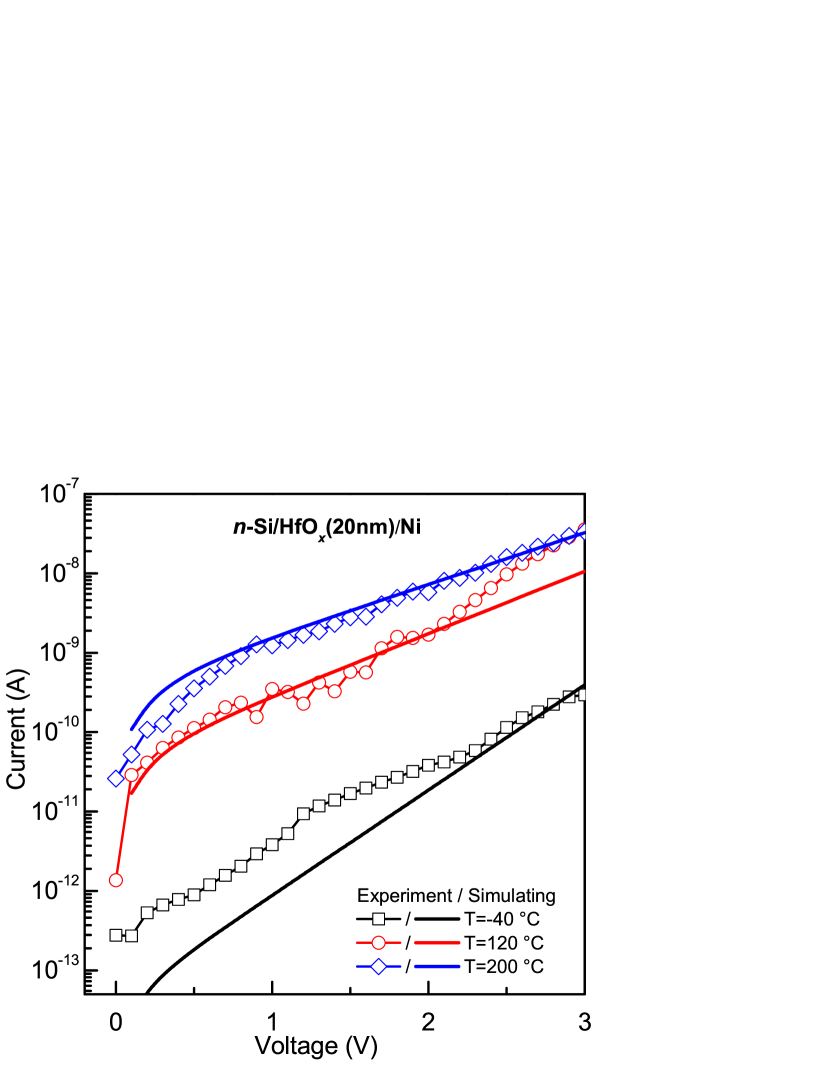
, is the energy of optical excitation of the trap, is the effective mass, is mean distance between traps. The results of this multi-parameter fitting procedure are shown in Fig.2, graphed in solid lines. This procedure yielded the values of different transport parameters, cm-3, eV, eV, and ( is a free electron mass). Quantitatively, there is full agreement between the model of phonon-assisted tunneling between traps and the experimental data. The trap thermal energy value of eV that was obtained is close to that of eV Takeuchi et al. (2004) and eV Jeong and Hwang (2005) observed earlier, and equal to a half of the Stokes luminescence shift Perevalov et al. (2014). Furthermore, the trap optical energy value of eV is close to the calculated value of eV for the negatively charged oxygen vacancy in hafnia reported earlier Muñoz Ramo et al. (2007b).
Fig. 3 shows the configuration diagram of a negatively charged oxygen vacancy (electron trap) in hafnia. A vertical transition with a value of eV corresponds to the optical trap excitation, transitions of eV correspond to thermal trap energy.

The same procedure was applied to experiment data of the charge transport measurements in MIS(ALD) and MIM structures. Experiment current-voltage characteristics compared with simulations in terms of the model of phonon-assisted tunneling between traps in MIS(ALD) are shown in Fig. 4. Fitting procedure returns the following parameters values: cm-3, eV, eV, and . Different values of fitting parameters of MIS(ALD) and MIS(ALD) structures have only the trap density and effective mass . The difference of effective mass values is due to bulk space charge (due to captured in traps electrons and holes), which is adequately addressed in Nasyrov et al. (2009). Neither thermal trap energy nor optical trap energy depend on film fabrication technology.
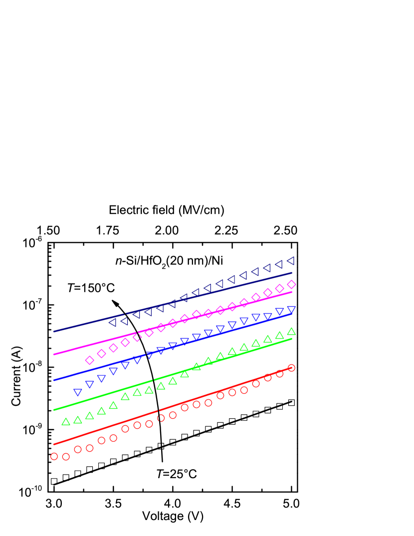
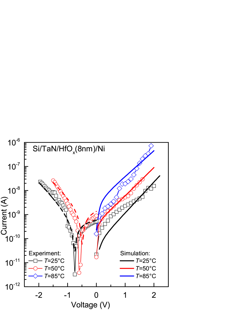
Fig. 5 shows the experimental data of current-voltage measurements in MIM structures at different temperatures. The solid lines present the results of simulations in terms of phonon-assisted tunneling between traps (3). MIM structures have the following parameter values: cm-3, eV, eV, and .
An artifact feature of experimental -- curves that the zero current is observed at non zero but negative voltages as shown in Fig. 5. This phenomenon is due to displacement current
| (4) |
is capacity of the sample, Vs is voltage sweep rate. Taking into account (4) in simulation of -- characteristics (1), (3) with found fitting parameters the artifact feature is described with good agreement as shown by dashed lines in Fig. 5.
The difference between different MIS ad MIM structures in effective mass is due to bulk space charge. However, it is important to notice that the trap’s energy parameters are invariants of grown structures and film fabrication techniques. Consequently, we found that the nature of charge carrier transport in hafnia and hafnia-based structures is phonon-assisted tunneling between traps. This charge transport model is more simple than based in quasi-continuous spectra of charge trap energy eV, proposed by L. Vandelli et al. Vandelli et al. (2011).
These results combined with spectra measurements and quantum chemical simulations Perevalov et al. (2014) show that namely oxygen vacancies are responsible for charge transport in \ceHfO_x, and the oxygen vacancies play the role or charge traps.
Previous experiments in charge transfer have demonstrated that hafnia conductivity is bipolar (or two-band) Islamov et al. (2011); Ando et al. (2011); Vandelli et al. (2011): electrons are injected from a negatively shifted contact in the dielectric, and holes are injected from a positively shifted electrode in the dielectric. For the reason of simplicity, the current study took into account electron conductivity only.
To summarize, we examined the transport mechanisms of \ceHfO2, demonstrating that transport in hafnium oxide is described by the model of phonon-assisted tunneling between traps. Simulating the current-voltage characteristics of this model and comparing experimental data with calculations revealed the energy parameters of the traps in hafnia: the thermal trap energy of eV and the optical trap energy of eV. Phonon-assisted tunneling between traps charge transport model describe experiment data results with excellent qualitative and quantitative agreement, while standard PF model has qualitative agreement only with unrealistic values for material parameters. These results jointly with earlier ones Perevalov et al. (2014) facilitated determining that oxygen vacancies act as charge carrier traps.
Our results can be used to predict the leakage currents in \ceHfO2-based devices and applications. High-quality MOSFET and FinFET transistors and SONOS flash memory require low leakage currents through the gate dielectrics and blocking insulator, while different states in resistive memory cells must be distinguishable over a wide range of temperatures. Temperature dependence of memory window (resistance ratio in different states) in resistive memory might be predicted as well.
This work was particularly supported by National Science Council, Taiwan (grant No. NSC103-2923-E-009-002-MY3) (growing test structures, preparing samples, performing transport measurements), and by the Russian Science Foundation (grant No. 14-19-00192) (calculations, modeling).
References
- Ma et al. (2005) T. P. Ma, H. M. Bu, X. W. Wang, L. Y. Song, W. He, M. Wang, H.-H. Tseng, and P. J. Tobin, IEEE Trans. Device Mater. Rel. 5, 36 (2005).
- Robertson (2006) J. Robertson, Reports on Progress in Physics 69, 327 (2006).
- Pavanello et al. (2007) M. A. Pavanello, J. A. Martino, E. Simoen, R. Rooyackers, N. Collaert, and C. Claeys, Solid-State Electronics 51, 285 (2007).
- Tsormpatzoglou et al. (2009) A. Tsormpatzoglou, D. H. Tassis, C. A. Dimitriadis, M. Mouis, G. Ghibaudo, and N. Collaet, Semiconductor Science and Technology 24, 125001 (2009).
- Chen et al. (2011) L.-J. Chen, Y.-C. Wu, J.-H. Chiang, M.-F. Hung, C.-W. Chang, and P.-W. Su, IEEE Trans. Nanotechnol. 10, 260 (2011).
- Tsai et al. (2009) P.-H. Tsai, K.-S. Chang-Liao, T.-C. Liu, T.-K. Wang, P.-J. Tzeng, C.-H. Lin, L. S. Lee, and M.-J. Tsai, IEEE Electron Device Lett. 30, 775 (2009).
- Yang et al. (2008) J. J. Yang, M. D. Pickett, X. Li, D. A. A. Ohlberg, D. R. Stewart, and R. S. Williams, Nature Nanotechnology 3, 429 (2008).
- Goux et al. (2010) L. Goux, P. Czarnecki, Y. Y. Chen, L. Pantisano, X. P. Wang, R. Degraeve, B. Govoreanu, D. J. Jurczak, M.and Wouters, and L. Altimime, Applied Physics Letters 97, 243509 (2010).
- Wang et al. (2012) Z. Wang, H. Y. Yu, X. A. Tran, Z. Fang, J. Wang, and H. Su, Physical Review B 85, 195322 (2012).
- Guha and Narayanan (2007) S. Guha and V. Narayanan, Physical Review Letters 98, 196101 (2007).
- Muñoz Ramo et al. (2007a) D. Muñoz Ramo, A. L. Shluger, J. L. Gavartin, and G. Bersuker, Physical Review Letters 99, 155504 (2007a).
- Foster et al. (2002) A. S. Foster, F. Lopez Gejo, A. L. Shluger, and R. M. Nieminen, Physical Review B 65, 174117 (2002).
- Zheng et al. (2007) J. X. Zheng, G. Ceder, T. Maxisch, W. K. Chim, and W. K. Choi, Physical Review B 75, 104112 (2007).
- Muñoz Ramo et al. (2007b) D. Muñoz Ramo, J. L. Gavartin, A. L. Shluger, and G. Bersuker, Physical Review B 75, 205336 (2007b).
- Jiang et al. (2010) H. Jiang, R. I. Gomez-Abal, P. Rinke, and M. Scheffler, Physical Review B 81, 085119 (2010).
- Xiong et al. (2005) K. Xiong, J. Robertson, M. C. Gibson, and S. J. Clark, Applied Physics Letters 87, 183505 (2005).
- Broqvist and Pasquarello (2006) P. Broqvist and A. Pasquarello, Applied Physics Letters 89, 262904 (2006).
- Perevalov et al. (2014) T. V. Perevalov, V. S. Aliev, V. A. Gritsenko, A. A. Saraev, V. V. Kaichev, E. V. Ivanova, and M. V. Zamoryanskaya, Applied Physics Letters 104, 071904 (2014).
- Sahoo and Misra (2011) S. K. Sahoo and D. Misra, Journal of Applied Physics 110, 084104 (2011).
- Pan et al. (2007) S. Pan, S.-J. Ding, Y. Huang, Y.-J. Huang, D. W. Zhang, L.-K. Wang, and R. Liu, Journal of Applied Physics 102, 073706 (2007).
- Zhu et al. (2002) W. J. Zhu, T.-P. Ma, T. Tamagawa, J. Kim, and Y. Di, IEEE Electron Device Lett. 23, 97 (2002).
- Lin et al. (2009) S. H. Lin, C. H. Cheng, F. S. Chen, W. B.and Yeh, and A. Chin, IEEE Electron Device Lett. 30, 999 (2009).
- Frenkel (1938) J. Frenkel, Physical Review 54, 647 (1938).
- Hill (1970) R. M. Hill, Philosophical Magazine 23, 59 (1970).
- Makram-Ebeid and Lannoo (1982) S. Makram-Ebeid and M. Lannoo, Physical Review B 25, 6406 (1982).
- Nasyrov and Gritsenko (2011) K. A. Nasyrov and V. A. Gritsenko, Journal of Applied Physics 109, 093705 (2011).
- Takeuchi et al. (2004) H. Takeuchi, D. Ha, and T.-J. King, Journal of Vacuum Science and Technology A 22, 1337 (2004).
- Jeong and Hwang (2005) D. S. Jeong and C. S. Hwang, Physical Review B 71, 165327 (2005).
- Nasyrov et al. (2009) K. A. Nasyrov, S. S. Shaimeev, V. A. Gritsenko, and J. H. Han, Journal of Applied Physics 105, 123709 (2009).
- Vandelli et al. (2011) L. Vandelli, A. Padovani, L. Larcher, R. G. Southwick, W. B. Knowlton, and G. Bersuker, IEEE Trans. Electron Devices 58, 2878 (2011).
- Islamov et al. (2011) D. R. Islamov, V. A. Gritsenko, C. H. Cheng, and A. Chin, Applied Physics Letters 99, 072109 (2011).
- Ando et al. (2011) T. Ando, N. D. Sathaye, K. V. R. M. Murali, and E. A. Cartier, IEEE Electron Device Lett. 32, 865 (2011).