Hybrid optical-electrical detection of donor electron spins with bound excitons in silicon
Abstract
Electrical detection of spins is an essential tool in understanding the dynamics of spins in semiconductor devices, providing valuable insights for applications ranging from optoelectronics[1, 2] and spintronics[3] to quantum information processing[4, 5, 6, 7, 8]. For electron spins bound to shallow donors in silicon, bulk electrically-detected magnetic resonance has relied on coupling to spin readout partners such as paramagnetic defects[6, 5] or conduction electrons[4, 7, 8] which fundamentally limits spin coherence times. Here we demonstrate electrical detection of phosphorus donor electron spin resonance by transport through a silicon device, using optically-driven donor-bound exciton transitions[9, 10]. We use this method to measure electron spin Rabi oscillations, and, by avoiding use of an ancillary spin for readout, we are able to obtain long intrinsic electron spin coherence times, limited only by the donor concentration[11]. We go on to experimentally address critical issues for adopting this scheme for single spin measurement in silicon nanodevices, including the effects of strain, electric fields, and non-resonant excitation. This lays the foundations for realising a versatile readout method for single spin readout with relaxed magnetic field and temperature requirements compared with spin-dependent tunneling[12, 13].
London Centre for Nanotechnology, University College London, London WC1H 0AH, UK.
Department of Electronic and Electrical Engineering, University College London, London WC1E 7JE, UK.
Hitachi Cambridge Laboratory, J. J. Thomson Avenue, Cambridge CB3 0HE, U.K.
Department of Electrical Engineering, Princeton University, Princeton, New Jersey 08544, USA.
Simon Fraser University, Burnaby, British Columbia V5A 1S6, Canada.
Shallow donor electron and nuclear spins in silicon have extraordinarily long coherence times[11, 9, 10], making them attractive candidates for quantum information processing[14], quantum memory[15], as well as for quantum sensing applications[16]. In addition, neutral shallow donors can form bound exciton states (D0X) with relatively long lifetimes (200–300 ns [17]) and correspondingly narrow intrinsic line widths, enabling optical transitions with both electron and nuclear spin selectivity[18]. D0X can be formed by a direct photon excitation (a no phonon transition) with energy 1.15 eV, below the silicon indirect bandgap of 1.17 eV. The photon excites an electron from the valence band at the neutral donor site, resulting in two indistinguishable electrons and one hole localised in the D0X ground state. The D0X state then relaxes via an Auger recombination process where the excess electron-hole pair recombines and its energy is transferred to the remaining electron, ejecting it from the donor site and leaving behind the positively charged donor ion.
The D0X spin-selective optical transitions are attractive for realising hybrid optical-electrical ensemble spin detection in silicon since no decoherence-inducing paramagnetic centre close to the dopant is required for spin-charge conversion. In addition, they could enable high-fidelity single dopant electron spin readout without the requirement of keeping the thermal energy much less than the Zeeman splitting — this is in contrast with spin-dependent tunneling schemes[12], where, for example, 80 electron spin readout fidelity was achieved at 300 mK and 1 T [13]. The maximum temperature for spin readout using D0X is limited by its dissociation energy of approximately 5 meV [19], such that this could be readily implemented at liquid helium temperatures. Spin readout fidelity is instead determined by the optical transition linewidths (approximately 20 neV when lifetime limited) compared to the D0X spin splitting, which is always at least the hyperfine interaction strength ( = 0.486 eV for phosphorus donors (31P)). Hence, zero magnetic field measurements are possible in principle. These strongly relaxed experimental conditions open the possibility of practical implementation of quantum sensing applications with donor spins[16], and enable access to the long donor spin relaxation times observed at low magnetic fields ( T) [11].
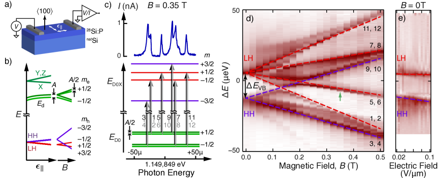
The D0X Auger recombination process has recently been used in conjunction with contact-less capacitive schemes in bulk silicon for the detection of nuclear spin coherence times in highly enriched 28Si [9, 10]. We apply this technique for electrical detection of D0X spectroscopy via direct transport measurements through devices built on epitaxially grown 28Si doped with 31P at cm-3 (see Fig. 1). The 28Si epitaxial layer has a built-in biaxial strain due to its lattice mismatch with the undoped substrate of natural isotope abundance[20]. The presence of strain modifies the local bandgap surrounding the donors by lifting the degeneracy of the valence and conduction band edges, and consequently shifts the donor binding energies through valley repopulation[21]. The states are further Zeeman split under an applied magnetic field, leading to six pairs of dipole-allowed transitions (), which we observe by monitoring the current through the device as the laser wavelength is swept. Due to the strain distribution in the epitaxial material and local strains induced by the electrical contacts, we do not resolve the hyperfine splitting of the 31P donors in this silicon device. By mapping out the magnetic field dependence of the D0X spectrum we obtain a complete picture of the valence band light hole (LH), heavy hole (HH) and Zeeman splittings, where the measured zero field splitting 19eV is due to the +2.410-6 (tensile) biaxial strain-induced LH-HH splitting. Assuming an isotropic -factor of for the 31P donor electrons[22], we find the D0X hole-state -factors to be 0.86 and 1.33 in this magnetic field orientation (), in good agreement with earlier measurements [23] (see Supplementary Information). Our device geometry allows us to study the effect of the LH-HH splitting as a function of electric field (Fig. 1(e)), yielding a linear Stark shift parameter of 2337eV/(V/m), or 0.8 Debye, similar to acceptor states in silicon[24]. Carrier injection from the electrical contacts prohibits measurements at larger electric fields.
To demonstrate electrical detection of electron spin resonance using D0X we set the magnetic field to 0.35 T and tuned our laser on resonance with transitions 5-6, as shown in Fig. 1(d). This optical excitation drives the spin-selective ionisation of spin-up electrons, after some time ( ms) leaving the donor electrons hyperpolarised into the spin-down state[18]. The laser excitation is turned off to allow coherent control of the donor spins via applied microwave pulses, and then turned on again for readout. Fig. 2(a) shows the measured current transients with, and without, a microwave pulse applied, illustrating how the difference in the integrated signals between the two is a measure of the donor spin -projection. Using this method we measure electron spin Rabi oscillations (Fig. 2(b)), demonstrating coherent manipulation and electrical detection of the donor spin states and yielding an ensemble dephasing time of 2s caused by the strain distribution in the sample.
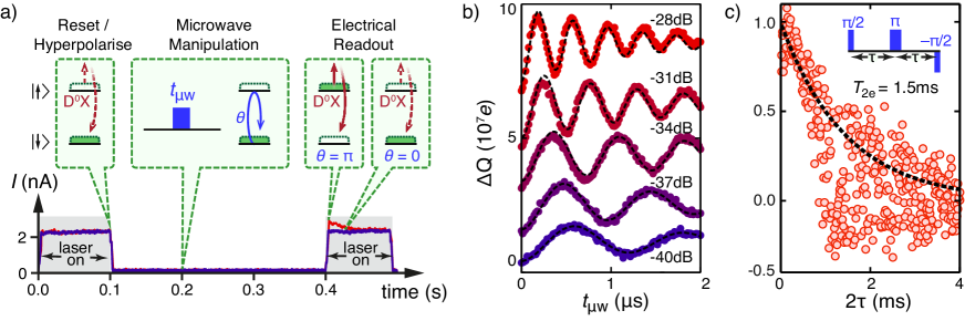
We measure the electron spin coherence time by implementing a two-pulse Hahn echo sequence with an additional pulse used to project the coherence into the population of the spin eigenstate (Fig. 2(c)). The fluctuations in signal amplitude after 1 ms are due to the presence of instrumental magnetic field noise so that only the period ms is fit to extract the spin coherence time. The measured value of ms is in good agreement with bulk spin resonance measurements for samples under similar dopant concentrations and isotopic purity[11], and reflects the advantage of utilising spin-selective optical transitions for electrical readout, as the donor spin coherence is no longer inherently limited by nearby sources of decoherence (e.g. s for spin-dependent recombination with interface paramagnetic defects[5]).
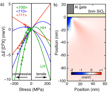
Below we address additional considerations for extending these results to realise single donor spin detection utilising neutral donor bound excitons, in particular the effects of i) strain and electric fields in nanodevices and ii) off-resonance optical excitation on readout fidelity. As observed in our silicon device, the D0X transition energies are extremely sensitive to local strains in the silicon crystal. This is further exemplified by the fact that the D0X inhomogeneous linewidth differs widely in bulk-doped electronic grade silicon crystals: 100eV for Czochralski silicon, 5eV for float-zone silicon and 0.2eV for high-quality isotopically enriched 28Si [18]. Figure 3(a) shows the change in D0X transition energies, [D0X], for 31P donors at zero magnetic field calculated from a single-particle perturbative model (see Supplementary Information for details) for uniaxial stresses up to 200 MPa ( 10-3 strain), which are not uncommon in silicon nanodevices[25]. The two branches for each stress direction are due to the valence band splitting as we have observed in our silicon device. Strain is inevitably present in qubit devices close to the silicon surface, where device-dependent strains can be introduced during the fabrication process, or due to the thermal expansion coefficient mismatch between gate or dielectric materials[25]. This is illustrated in Figure 3(b), showing calculated [D0X] due to the thermal expansion coefficient mismatch problem for 31P donors in close proximity to aluminium gate electrodes. The presence of metallic gates and the insulating oxide strains the silicon substrate considerably, and the uncertainty in dopant positioning can cause a large detuning of the transition energies that are orders of magnitude greater than the spin splitting, limiting the ability to address arrays of single dopant devices in a scaled qubit architecture. This sensitivity to strain is more severe for D0X than for optical transitions of erbium ions in silicon[26], where only core shell electronic levels are involved.
The electric fields present in silicon nanodevices will also shift the D0X energy, as we have already shown above through the Stark splitting of the hole states. However, if the field is particularly strong, it is expected to additionally reduce the bound exciton lifetime in an analogous process to field ionisation of donors, but taking into account the much lower binding D0X energy of 5 meV. Therefore, both strain and electric fields in realistic single dopant devices must be carefully considered and controlled for the successful implementation of D0X-based spin readout.
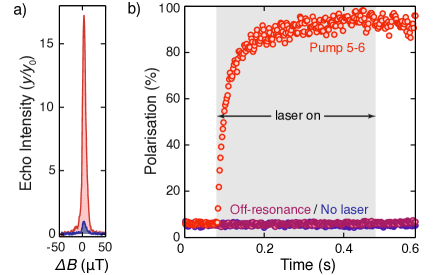
Two important factors impacting electron spin readout fidelity using this approach are the ability to detect the resonantly-formed ionised donor state (e.g. using a charge sensor) and false readings arising from non-resonant ionisation events. The former is unlikely to be limiting as bound excitons can be resonantly generated at a much faster rate than typical spin relaxation times (85 MHz in our experimental set up, see Supplementary Information), and once ionised, the dopant neutralisation time is in the order of 10 ms (depending strongly on the concentration of free carriers) which is ample time for charge state detection. On the other hand, non-resonant ionisation of the donor state can be caused by off-resonance photons directly ionising neutral donors, or creating free excitons which subsequently recombine at neutral donor sites (we note, however, the energy required for free exciton formation is approximately 5 meV higher than resonant D0X transitions in bulk silicon). We examine the role of non-resonant irradiation in more detail below by observing its effect on bulk electron spin resonance (ESR) measurements. We first show the electron spin hyperpolarisation through the ESR signal enhancement seen for an echo-detected field sweep, with and without a laser pulse tuned to the 5-6 D0X transition (Fig. 4(a)). The dynamics of this process can be seen by mapping out the echo intensity at different times during the laser pulsing sequence, as shown in Fig. 4(b). The echo intensities are normalised with respect to the thermal equilibrium signal, and when the laser pulse is on resonance, the maximum electron spin polarisation achieved is close to 100 (see Supplementary Information). Conversely, when the laser is detuned away from resonance by 3eV, the echo intensity remains constant and identical to the thermal equilibrium measurement. This demonstrates that off-resonant ionisation is negligible in dilutely doped substrates (as both direct ionisation and free exciton-donor recombination would diminish the echo intensity) and hence is unlikely to pose a major limit on electron spin readout fidelity. Nevertheless, if non-resonant ionisation is found to affect readout fidelity to some degree, the donor nuclear spin could be used as an ancilla for performing repetitive measurements[28].
A hybrid optical-electrical single donor detection scheme utilising donor bound excitons coupled to a quantum point contact has been previously proposed[29], however, the uncertainty in local strain and relatively large electric fields present in metal-oxide-semiconductor based architectures will make measuring bound excitons difficult. While D0X detection can conversely be used as an extremely sensitive probe to quantify strain and electric fields of silicon nanostructures and devices in the atomistic scale, reducing these perturbative field distributions will be crucial for implementing hybrid optical-electrical detection for large arrays of qubit devices on a single chip. Therefore, an optimally designed readout device should have both the strain and electric fields carefully controlled (and minimised) in the vicinity of the dopant. For instance, epitaxially-grown[30] or nanowire single electron transistors operating at liquid helium temperatures can be used as the charge detector, and in this hybrid spin detection scheme the need for dilution refrigerators can be completely alleviated, opening the door for exploiting ultra-long coherent donor spins for practical quantum technological applications.
We thank A.M. Tyryshkin for useful discussions. This research is supported by the EPSRC through the Materials World Network (EP/I035536/1) and UNDEDD project (EP/K025945/1) as well as by the European Research Council under the European Community’s Seventh Framework Programme (FP7/2007-2013)/ERC grant agreement No. 279781. Work at Princeton was supported by NSF through Materials World Network (DMR-1107606) and through the Princeton MRSEC (DMR-0819860). C.C.L. is supported by the Royal Commission for the Exhibition of 1851. J.J.L.M. is supported by the Royal Society.
References
- [1] H. Malissa, M. Kavand, D. P. Waters, K. J. van Schooten, P. L. Burn, Z. V. Vardeny, B. Saam, J. M. Lupton, and C. Boehme. Room-temperature coupling between electrical current and nuclear spins in OLEDs. Science, 345(6203):1487–1490, 2014.
- [2] Michael Algasinger, Julie Paye, Florian Werner, Jan Schmidt, Martin S. Brandt, Martin Stutzmann, and Svetoslav Koynov. Improved black silicon for photovoltaic applications. Advanced Energy Materials, 3(8):1068–1074, 2013.
- [3] I. Appelbaum, B. Huang, and D. J. Monsma. Electronic measurements and control of spin transport in silicon. Nature, 447:295, 2007.
- [4] D. R. McCamey, J. van Tol, G. W. Morley, and C. Boehme. Electronic spin storage in an electrically readable nuclear spin memory with a lifetime 100 seconds. Science, 330:1652, 2010.
- [5] S. Y. Paik, S. Y. Lee, W. J. Baker, D. R. McCamey, and C. Boehme. and spin relaxation time limitations of phosphorus donor electron near crystalline silicon to silicon dioxide interface defects. Physical Review B, 81(7):075214, 2010.
- [6] A. R. Stegner, C. Boehme, H. Huebl, M. Stutzmann, K. Lips, and M. S. Brandt. Electrical detection of coherent 31P spin quantum states. Nature Physics, 2:835, 2006.
- [7] C. C. Lo, V. Lang, R. E. George, J. J. L. Morton, A. M. Tyryshkin, S. A. Lyon, J. Bokor, and T. Schenkel. Electrically detected magnetic resonance of neutral donors interacting with a two-dimensional electron gas. Physical Review Letters, 106(20):207601, 2011.
- [8] C. C. Lo, C. D. Weis, J. van Tol, J. Bokor, and T. Schenkel. All-electrical nuclear spin polarization of donors in silicon. Physical Review Letters, 110(5):057601, 2013.
- [9] M. Steger, K. Saeedi, M. L. W. Thewalt, J. J. L. Morton, H. Riemann, N. V. Abrosimov, P. Becker, and H. J. Pohl. Quantum information storage for over 180s using donor spins in a 28Si “semiconductor vacuum”. Science, 336:1280, 2012.
- [10] K. Saeedi, S. Simmons, J.Z. Salvail, P. Dluhy, H. Riemann, N. V. Abrosimov, P. Becker, H.-J. Pohl, J. J. L. Morton, and M. L. Thewalt. Room-temperature qubit storage exceeding 39 minutes using ionized donors in 28si. Science, 342:830, 2013.
- [11] A. M. Tyryshkin, S. Tojo, J. J. L. Morton, H. Riemann, N. V. Abrosimov, P. Becker, H. J. Pohl, T. Schenkel, M. L. W. Thewalt, K. M. Itoh, and S. A. Lyon. Electron spin coherence exceeding seconds in high-purity silicon. Nature Materials, 11(2):143, 2012.
- [12] A. Morello, J. J. Pla, F. A. Zwanenburg, K. W. Chan, K. Y. Tan, H. Huebl, M. Möttönen, C. D. Nugroho, C. Yang, J. A. van Donkelaar, A. D. C. Alves, D. N. Jamieson, C. C. Escott, L. C. L. Hollenberg, R. G. Clark, and A. S. Dzurak. Single-shot readout of an electron spin in silicon. Nature, 467:687, 2010.
- [13] J. J. Pla, K. Y. Tan, J. P. Dehollain, W. H. Lim, J. J. L. Morton, D. N. Jamieson, A. S. Dzurak, and A. Morello. A single-atom electron spin qubit in silicon. Nature, 489:541, 2012.
- [14] B. Kane. A silicon-based nuclear spin quantum computer. Nature, 393:133, 1998.
- [15] J. J. L. Morton, A. M. Tyryshkin, R. M. Brown, S. Shankar, B. W. Lovett, A. Ardavan, T. Schenkel, E. E. Haller, J. W. Ager, and S. A. Lyon. Solid-state quantum memory using the 31P nuclear spin. Nature, 455(7216):1085, 2008.
- [16] J.M. Taylor, P. Cappellaro, L. Childress, L. Jiang, D. Budker, P.R. Hemmer, A. Yacoby, R. Walsworth, and M.D. Lukin. High-sensitivity diamond magnetometer with nanoscale resolution. Nature Physics, 4:810, 2008.
- [17] W. Schmid. Auger lifetimes for excitons bound to neutral donors and acceptors in Si. Phys. Stat. Sol. (b), 84:529, 1977.
- [18] A. Yang, M. Steger, T. Sekiguchi, M. L. W. Thewalt, T. D. Ladd, K. M. Itoh, H. Riemann, N. V. Abrosimov, P. Becker, and H.-J. Pohl. Simultaneous sub second hyper polarization of the nuclear and electron spins of phosphorus in silicon by optical pumping of exciton transitions. Physical Review Letters, 102(25):257401, 2009.
- [19] J. R. Haynes. Experimental proof of the existence of a new electronic complex in silicon. Physical Review Letters, 4:361, 1960.
- [20] A. Yang, M. Steger, H. J. Lian, M. L. W. Thewalt, M. Uemura, A. Sagara, K. M. Itoh, E. E. Haller, J. W. Ager III, S. A. Lyon, M. Konuma, and M. Cardona. High-resolution photoluminescence measurement of the isotopic-mass dependence of the lattice parameter of silicon. Physical Review B, 77:113203, 2008.
- [21] D. K. Wilson and G. Feher. Electron spin resonance experiments on donors in silicon. III. Investigation of excited states by the application of uniaxial stress and their importance in relaxation processes. Physical Review, 124(4):1068, 1961.
- [22] G. Feher. Electron spin resonance experiments on donors in silicon. I. Electronic structure of donors by electron nuclear double resonance technique. Physical Review, 114(5):1219, 1959.
- [23] A. S. Kaminskii, V. A. Karasyuk, and Ya. E. Pokrovskii. Luminescence of excitons bound to phosphorus atoms in silicon subjected to a magnetic field. Sov. Phys. JETP, 52:211, 1980.
- [24] A. Kopf and K. Lassmann. Linear stark and nonlinear zeeman coupling to the ground state of effective mass acceptors in silicon. Physical Review B, 69:1580, 1992.
- [25] T. Thorbeck and N. M. Zimmerman. Formation of strain-induced quantum dots in gated semiconductor nanostructures. arXiv:1409.3549v1, 2014.
- [26] C. Yin, M. Rancic, G. G. de Boo, N. Stavrias, J. C. McCallum, M. J. Sellars, and Sven Rogge. Optical addressing of an individual erbium ion in silicon. Nature, 497:91, 2013.
- [27] M L. W. Thewalt and J. A. Rostworowski. Multiexciton complexes bound to phosphorus in silicon. Physical Review Letters, 41:808, 1978.
- [28] L. Jiang, J. S. Hodges, J. R. Maze, P. Maurer, J. M. Taylor, D. G. Cory, P. R. Hemmer, R. L. Walsworth, A. Yacoby, A. S. Zibrov, and M. D. Lukin. Repetitive readout of a single electronic spin via quantum logic with nuclear spin ancillae. Science, 326:267, 2009.
- [29] D. Sleiter, N. Y. Kim, K. Nozawa, T. D. Ladd, M. L. W. Thewalt, and Y. Yamamoto. Quantum hall charge sensor for single-donor nuclear spin detection in silicon. New Journal of Physics, 12:093028, 2010.
- [30] A. Fuhrer, M. Fchsle, T. C. G. Reusch, B. Weber, and M. Y. Simmons. Atomic-scale, all epitaxial in-plane gated donor quantum dot in silicon. Nano Letters, 9(2):707, 2009.