,
Low carrier concentration crystals of the topological insulator Bi2-xSbxTe3-ySey: a magnetotransport study
Abstract
In 3D topological insulators achieving a genuine bulk-insulating state is an important research topic. Recently, the material system (Bi,Sb)2(Te,Se)3 (BSTS) has been proposed as a topological insulator with high resistivity and a low carrier concentration (Ren et al. [1]). Here we present a study to further refine the bulk-insulating properties of BSTS. We have synthesized Bi2-xSbxTe3-ySey single crystals with compositions around and . Resistance and Hall effect measurements show high resistivity and record low bulk carrier density for the composition Bi1.46Sb0.54Te1.7Se1.3. The analysis of the resistance measured for crystals with different thicknesses within a parallel resistor model shows that the surface contribution to the electrical transport amounts to 97 % when the sample thickness is reduced to m. The magnetoconductance of exfoliated BSTS nanoflakes shows 2D weak antilocalization with as expected for transport dominated by topological surface states.
Keywords: Topological insulator, Magnetotransport, Surface states, Weak anti-localization
pacs:
72.20.My, 73.25.+i, 74.62.Dh1 Introduction
Three dimensional (3D) topological insulators (TIs) have generated intense research interest, because they offer unmatched opportunities for the realization of novel quantum states [2, 3]. Theory predicts the interior of the TI sample (the bulk) is insulating, while the metallic surface states have a Dirac cone dispersion and a helical spin structure. Because of time reversal symmetry and a strong spin-orbit interaction, the surface charge carriers are insensitive to backscattering from non-magnetic impurities and disorder. This makes TIs promising materials for a variety of applications, ranging from spintronics and magnetoelectrics to quantum computation [4, 5, 6]. The topological surface states of exemplary TIs, such as Bi1-xSbx, Bi2Te3, Bi2Se3, Sb2Te3, etc., have been probed compellingly via surface-sensitive techniques, like angle-resolved photoemission spectroscopy (ARPES) [7, 8, 9, 10] and scanning tunneling microscopy (STM) [11, 12]. However, the transport properties of the surface states turn out to be notoriously difficult to investigate, due to the dominant contribution from the bulk conduction resulting from intrinsic impurities and crystallographic defects. At the same time, potential applications strongly rely on the tunability and robustness of charge and spin transport at the device surface or interface. Therefore, achieving surface-dominated transport in the current families of TI materials remains a challenging task, in spite of the progress that has been made recently, including charge carrier doping [13, 14], thin film engineering and electrostatic gating [15, 16].
Recently, it was reported that the topological material Bi2Te2Se exhibits variable range hopping (VRH) behavior in the transport properties, which leads to high resistivity values exceeding cm at low temperatures [17]. This ensures the contribution from the bulk to electrical transport is small. At the same time the topological nature of the surface states was probed by Shubnikov - de Haas oscillations [17, 18]. Further optimizing studies include different crystal growth approaches [19], Bi excess [20] and Sn doping [21, 22]. Bi2Te2Se has an ordered tetradymite structure (spacegroup R3̄m) with quintuple-layer units of Te-Bi-Se-Bi-Te with the Te and Se atoms occupying distinct lattice sites. Next the composition of Bi2Te2Se was optimized by Ren et al. [1] by reducing the Te:Se ratio and introducing Sb on the Bi sites. An extended scan of isostructural Bi2-xSbxTe3-ySey (BSTS) solid solutions resulted in special combinations of and , notably and , where the resistivity attains values as large as several cm at liquid helium temperature. In addition values of the bulk carrier concentration as low as 2 cm-3 were achieved [23]. The topological properties of BSTS samples with and near these optimized values were subsequently examined by a number of techniques, like ARPES [24], terahertz conductivity [25], and STM and STS [26, 27].
In this paper we report an extensive study conducted to confirm and further investigate the bulk-insulating properties of Bi2-xSbxTe3-ySey with and around 0.5 and 1.3, respectively. In the work of Ren et al. [1] the BSTS composition was scanned with a step size and of typically 0.25. For our study we prepared single crystals with much smaller step sizes, typically and . Magnetotransport measurements showed that the carrier type in Bi2-xSbxTe1.7Se1.3 changes from hole to electron when , while the carrier type remains unchanged in Bi1.46Sb0.54Te3-ySey when is varied from 1.2 to 1.6. The composition Bi1.46Sb0.54Te1.7Se1.3 presented the highest resistivity (12.6 cm) and lowest bulk carrier density ( cm-3) at K.
In addition, the effect of reducing the sample thickness on the ratio between the surface and bulk conductivity was investigated. For this study we used the composition Bi1.46Sb0.54Te1.4Se1.6 and gradually thinned down a 140 m thick sample to 6 m. The analysis of the resistance data in terms of a two-resistor model reveals the surface contribution to the total conductivity can be as large as 97 % at K when the sample thickness is 1 m. The angular variation of the magnetoconductance of a nanoflake with composition Bi1.46Sb0.54Te1.7Se1.3 shows a pronounced weak antilocalization (WAL) term, whose field dependence followed the Hikami-Larkin-Nagaoka formula [28] with a fit parameter close to -1 as expected for topological surface states [29]. We conclude that good quality BSTS single crystals can be achieved via careful compositional variation and thickness reduction such that the topological surface transport overwhelms the bulk conduction channel.
2 Methods
High quality Bi2-xSbxTe3-ySey single crystals were obtained by melting stoichiometric amounts of the high purity elements Bi (99.999 %), Sb (99.9999 %), Te (99.9999 %) and Se (99.9995 %). The raw materials were sealed in an evacuated quartz tube which was vertically placed in the uniform temperature zone of a box furnace. Both this choice of growth approach and our choice to keep the growth boules of small size (maximal dimension 1 cm) were made so as to maximise the homogeneity within each single crystal run. The molten material was kept at 850 ∘C for 3 days and then cooled down to 520 ∘C with a speed of 3 ∘C/h. Next the batch was annealed at 520 ∘C for 3 days, followed by cooling to room temperature at a speed of 10 ∘C/min. In the following all - and -values refer to nominal concentrations. Electron probe microanalysis (EPMA) carried out on six crystals selected within the series showed the nominal compositions to be in good agreement with the stoichiometry in the final single crystals produced. In addition, EPMA showed there to be no observable spatial inhomogeneity across the sample, which is in keeping with the homogeneous secondary electron images the crystals gave and the lack of any measurable impurity phases seen in standard x-ray diffraction characterisation of the samples. The systematic thickness dependence reported in the following also argues for an acceptable level of sample homogeneity. The as-grown platelet-like single crystals were cleaved with Scotch tape parallel to the -plane to obtain flat and shiny surfaces at both sides. Care was taken to maintain a sample thickness of m for all samples. Next the samples were cut into a rectangular shape using a scalpel blade. For the transport measurements in a five-probe configuration, thin (50 m) copper wires were attached to the samples using silver paint. Current and voltage contacts were made at the edges of the sample to ensure contact with the bulk and the upper and lower surface. The exposure time to air between cleaving and mounting the samples in the cryostat was kept to a minimum of about 1 h.
Four-point, low-frequency, ac-resistivity and Hall effect measurements were performed in a MaglabExa system (Oxford Instruments) equipped with a 9 T superconducting magnet in the temperature range from 4 to 300 K. The excitation current was typically 1000 A. Selected measurements were spot-checked using a PPMS system (Dynacool, Quantum Design) with 100 A excitation current. Measurements were always made for two polarities of the magnetic field after which the Hall resistance, , and longitudinal resistance, , were extracted by symmetrization. When investigating the effect of the sample thickness, layers were removed from the sample by Scotch tape. Special care was taken to maintain a uniform thickness across the sample, as well as the same lateral dimensions. For the thickness-dependent series, the resistance measurements were made in a bath cryostat in the temperature range 4.2-300 K using an AC Resistance Bridge (Model 370, LakeShore Cryotronics).
For our investigation of the WAL effect, flakes of thickness in the range of 80 to 200 nm were mechanically exfoliated on silicon-on-insulator substrates. Au Hall bar electrodes were prepared by standard photolithography followed by e-beam lithography and argon ion etching to shape the flake in a Hall bar structure. During the fabrication steps we covered the devices with e-beam or photoresist to avoid damaging and contamination of the surface. The Hall bars have a total length of 24 m and have widths in the range of 0.5-2.0 m. Transport measurements on these samples were carried out in a PPMS (Dynacool, Quantum Design) in the temperature range 2-300 K with an excitation current of 5 A. The field-angle dependence of WAL was measured for a rotation of the Hall bar around its long axis (the current direction).
ARPES measurements were carried out on cleaved single crystals of Bi2Se3 and Bi1.46Sb0.54Te1.7Se1.3 at the SIS beamline of the Swiss Light Source at the Paul Scherrer Institute. The photon energies used were 27 and 30 eV, and the sample temperature was 17 K. In both cases, the surfaces were exposed to sufficient residual gas such that the downward band bending – as documented in [30, 31] for Bi2Se3 – has saturated and thus was no longer changing as a function of time. The energy resolution was 15 meV.
3 Results and analysis
3.1 Composition variation
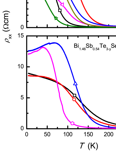
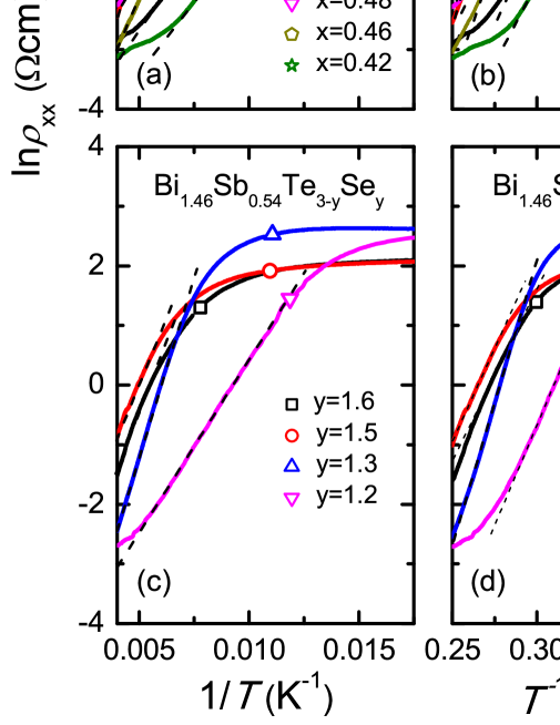
In this section we present the resistivity, , and Hall effect, , data. Rather than simply re-growing the optimal -values of (0.5,1.3) reported by Ren et al. [1], we first varied from 0.42 to 0.58 while keeping fixed at 1.3. Next, we fixed at 0.54 and varied from 1.2 to 1.6. The size of the steps taken in both and were smaller than those reported earlier. The temperature variation of the resistivity for these two series of crystals is shown in Figure 1a and Figure 1b, respectively. All the samples display an overall similar resistivity behavior. Upon cooling below 300 K the resistivity increases first slowly and then faster below K till reaches a maximum value at 50-100 K. Next the resistivity shows a weak decrease and levels off towards 4 K. The increase of the resistivity can be described by an activated behavior where is the activation energy, followed by a 3D VRH regime where is a constant [1]. These different regimes show considerable overlap as illustrated in Figure 2a and 2b, and in Figure 2c and 2d. Below K the resistivity is described by a parallel circuit of the insulating bulk and the metallic surface states (see the next section).
| Composition | K | K | K | K | K | K | |
|---|---|---|---|---|---|---|---|
| Bi2-xSbxTe3-ySey | (mcm) | (cm) | (meV) | (cm3/C) | (cm3/C) | (1016 cm-3) | (cm2/Vs) |
| ; | \050.5 | 10.4 | \044 | \m— | \0-468 | \0\01.3 | \045 |
| ; | \053.6 | 12.6 | 102 | \030 | -3110 | \0\00.2 | 247 |
| ; | 141 | \07.1 | \056 | \027 | \0\0380 | \0\01.6 | \054 |
| ; | \081.9 | \05.5 | \048 | \020 | \0-167 | \0\03.7 | \030 |
| ; | \036.6 | \05.0 | \072 | \031 | \01657 | \0\00.4 | 331 |
| ; | \044.4 | \06.8 | \036 | \0\04 | \0\0\0\06 | 107 | \0\00.9 |
| ; | 133 | \08.6 | \083 | -92 | \0-707 | \0\00.9 | \082 |
| ; | 214 | \08.9 | \066 | \037 | \0-278 | \0\02.2 | \031 |
| ; | \m— | 12.1 | \048 | \0\08 | -1940 | \0\00.3 | 160 |
In Table 1 we have collected the -values at 280 K and 4 K and the activation energy for a number of samples. The data in this table represent the summary of 35 individual measurements, 15 of which were carried out on the and composition. The resistivity values at K all exceed cm. We remark that in our first series of crystals with a fixed value the sample with has a record-high -value of cm at K, and the largest value meV as well. Subsequent small changes of in the range 1.2-1.6 did not yield a further increase of the low temperature resistivity.
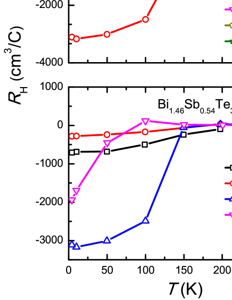
Given these resistivity data, Hall experiments are of interest to examine the character and quantity of bulk carriers in these samples. The temperature variation of the low-field Hall coefficient for the two series of crystals with fixed and fixed is shown in Figure 3a and 3b, respectively. The Hall coefficients were obtained by fitting the linear Hall resistivity for T. For the first series (Figure 3a), of all samples is positive at temperatures above 200 K and the values gradually increase upon lowering the temperature. Near 150 K, i.e. near the temperature where the resistivity starts to rise quickly, the absolute value of the Hall coefficient increases rapidly. For an increasing Sb content with respect to , turns negative, whereas for a decreasing Sb content remains positive. For the second series of samples (Figure 3b) of all samples starts positive near room temperature, but eventually attains fairly large negative values near 4 K.
The carrier type and concentration in BSTS and related compounds is in general connected to the competition between two effects: (i) (Bi,Sb)/Te antisite defects which act as electron acceptors (or hole dopants), and (ii) Se vacancies which act as electron donors. This tells us that in the high temperature regime where (Bi,Sb)/Te antisite defects are dominant in providing carriers. However, at low temperatures and Se vacancies prevail, except for the crystals with a reduced Sb content (). -values at 200 K and 4 K are listed in Table 1. In order to compare the transport parameters with values reported in the literature we have listed the bulk carrier density, , and mobility as well, assuming a simple single band model. Clearly, in these data, the crystal with the composition Bi1.46Sb0.54Te1.7Se1.3 stands out as the one with the highest resistivity, the largest activation gap and the lowest carrier concentration cm-3.
We grew three batches of single crystals of this composition and the measurement of 15 single crystals of Bi1.46Sb0.54Te1.7Se1.3 gave a reproducible picture that this composition generally gave the most bulk-insulating behaviour. There is some sample to sample variation in the transport parameters. For example, the low-T resistivity for the / composition of 12.6 cm given in Table 1 was representative, but values were also measured to be in the range of 11-15 cm.
3.2 Thickness variation
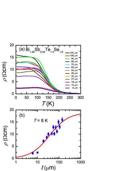
A simple and elegant way to separate the contribution from the surface and the bulk to the total conductivity of a topological insulator is by reducing the sample thickness, [23, 32, 33, 34]. In Figure 4a we show the resistivity of a Bi1.46Sb0.54Te1.4Se1.6 crystal with m that subsequently was thinned down in 12 steps to 6 m. Here where is the cross sectional area for the current ( is the sample width) and the distance between the voltage contacts. The overall behavior for all thicknesses is similar to the results presented in Figure 1. However, while the curves almost overlap at high temperatures, the -value at low temperatures decreases significantly when reducing the sample thickness. This tells us the ratio between the surface and bulk contribution changes with thickness.
For a proper analysis the parallel resistor model is used:
| (1) |
where and are the resistivities, and and the thicknesses, of the bulk and the surface layer [1], respectively. For we may take 3 nm which is the thickness of 1 unit cell. The factor 2 in the equation above counts the top and the bottom surface of the sample. In Figure 4b we have traced taken at 8 K as a function of . The uncertainty in the -values is mainly due to the error in the geometrical factor, especially in the value of (%) because of the finite size of the silver paint contacts. The solid line represents a least square fit to Equation 1 with fit parameters cm and cm, or expressed as conductivities cm-1 and cm-1. Consequently, the surface conductance . We remark our value for compares favorably to (is smaller than) the values 0.1 cm-1 and 0.12 cm-1 for sample compositions Bi1.5Sb0.5Te1.7Se1.3 and Bi1.5Sb0.5Te1.8Se1.2 reported in [23] and [32], respectively. The ratio of the surface conductance over the total sample conductance can be calculated as . With our fit parameters we calculate for samples with a thickness of 100, 10 and 1 m a surface contribution of 27 %, 78 % and 97 %, respectively. For a nanoflake with typical thickness of 130 nm (see the next section), we obtain a value of 99.6 %. We conclude surface-dominated transport can be achieved in our BSTS crystals grown with a global composition Bi1.46Sb0.54Te1.4Se1.6 when the sample thickness is less than m.
3.3 Weak antilocalization
The thickness dependence of the resistivity shows dominance of surface transport for thin samples. A further test as to whether the surface dominated transport is consistent with the presence of topological surface conduction channels is to search for and characterise possible signals of weak antilocalization. For our study of weak antilocalization we selected the BSTS composition we found to give crystals with the highest bulk resistivity: Bi1.46Sb0.54Te1.7Se1.3. The magnetoresistance of an exfoliated nanoflake, structured by e-beam lithography into a Hall bar, was measured in the temperature range 2-40 K and in magnetic fields up to 2 T. The dimensions of the Hall bar are: thickness nm, channel width m and distance between the voltage contacts m. The error in takes into account the extended size of the voltage electrodes. The temperature variation of the resistivity of the Hall bar is shown in the inset of Figure 5b. For this thickness the resistivity at low temperatures levels off at a low value of cm, in good agreement with the functional behavior reported in Figure 4b for BSTS with a Se content . Since we obtain a sheet or surface conductance .
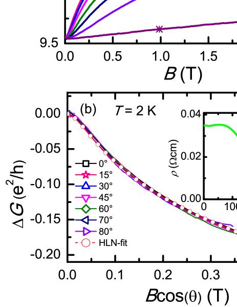
In Figure 5a we show the resistance, , as a function of , measured at K. The relatively sharp increase of with field is ubiquitous in TIs [35, 29, 36] and is attributed to the suppression of 2D weak antilocalization, i.e. the constructive interference of time reversed scattering loops, generated by a magnetic field applied perpendicular to the sample surface, . As the analysis of the magnetoresistance data we carry out below will show, the phase coherence length for the WAL in this system is of the same order as the flake thickness, justifying a double-check that the WAL behavior is indeed two-dimensional by recording the angular dependence of the WAL. In Figure 5a, the magnetoresistance, (we have dropped the subscript ) is seen to be largest for perpendicular to the sample surface (). For an in-plane magnetic field () a small residual magnetoresistance is seen of unknown origin, but this has essentially no effect on the parameters coming out of the fits to the data presented and discussed in the following. In Figure 5b we trace the magnetoconductance for as a function of . Obviously, the data collapse onto an universal curve, which signals the two dimensional character of the WAL in these samples.
| Composition | Thickness | Temperature | Reference | |||
|---|---|---|---|---|---|---|
| Bi2-xSbxTe3-ySey | (nm) | (T) | (nm) | (K) | ||
| ; | 130 | 0.5 | 116 | -1.14 | \02 | this work |
| ; | 130 | 0.5 | \052 | -0.93 | 40 | this work |
| ; | 200 | 0.5 | 121 | -0.96 | \02 | [37] |
| ; | 596 | 0.5 | 160 | -0.75 | \02 | [32] |
| ; | \085 | 6 | 170 | -1.3 | \04 | [38] |
Next we compare the universal curve with the expression for the magnetoconductivity of 2D weak antilocalization put forward by Hikami, Larkin and Nagaoka (HLN) [28]:
| (2) |
Here is the digamma function, is the effective phase coherence length and is a prefactor. Each scattering channel from a band that carries a Berry phase contributes a value [29]. For independent bottom and top topological surface channels we therefore expect . In Equation 2, , where . We have fitted the collapsed magnetoconductance data at K to the HLN expression with and as fit parameters. In the field interval T we find nm and . For this value of we calculate T and the condition is easily met, i.e. the applied field is sufficiently large to suppress WAL. Furthermore, which ensures our Hall bar has the proper dimensions for 2D WAL. If we extend the field range of the fit, the value of decreases slightly, but at the same time the quality of the fit decreases. For instance, by fitting up to 2 T we obtain .
The temperature variation of the field-induced suppression of WAL has been investigated at and K. By increasing the temperature the WAL becomes weaker and is suppressed more easily by the magnetic field. By fitting our collapsed curves, decreases to 52 nm at K. A power-law fit yields in the temperature range 10-40 K, which is close to the expected behavior for 2D WAL. However, below 10 K levels off and the exponent drops to -0.06. The prefactor decreases slightly to at 40 K for a fit range T.
4 Discussion
Single crystals of Bi2-xSbxTe3-ySey with and around 0.5 and 1.3 can nowadays clearly be considered to have superior bulk insulating properties [1, 23, 32, 37, 38] amongst the 3D topological insulators. This makes BSTS particularly attractive for exploratory research into TI devices with functionalities based on protected surface transport. In this paper we have shown that by fine tuning the BSTS composition it is possible to obtain record high values of the resistivity. For a global composition of Bi1.46Sb0.54Te1.7Se1.3 low-T resistivity values exceeding cm were common for samples with a thickness of 100 m. At the same time Hall data show the bulk carrier concentration in these samples can be as low as cm-3 at K. The strong bulk insulating behavior is furthermore demonstrated by the large value of the activation gap for transport, meV. The data of Table 1 show there to be a non-trivial dependence of the transport characteristics on the and -values chosen for each single crystal batch. Our sample characterization shows that this is clearly not a consequence of random compositional irreproducibility from sample to sample. Rather, the chemistry controlling the defect density and balance (between p- and n-type) in these low-carrier concentration 3D TI materials is a subtle quantity, and not one that simply tracks the Bi/Sb and Te/Se ratios in a linear fashion. This makes a variation of composition necessary to determine the best route to the most bulk insulating behaviour. This was done in Ref. [1] and is also the approach adopted here, resulting in excellent bulk-insulating characteristics.
Because of the genuine bulk insulating behavior of the optimized BSTS crystals, the -values obtained at low temperatures are not true resistivity values but depend on the thickness when mm (see Figure 4). Therefore the transport data result from parallel channels due to the bulk and top/bottom surfaces. Our analysis with the parallel resistor model of the resistance measured on the very same BSTS crystal made thinner and thinner shows that the surface contribution to the total transport is close to 97 % for a thickness of m. Hence we conclude that devices fabricated with submicrometer thickness are sufficiently bulk insulating to exploit the topological surface states by transport techniques. The nanoflake with a thickness of 130 nm certainly fulfills this condition.
The HLN fit of the magnetoconductance of the thin flake yields values of close to -1, which is in keeping with the thickness dependence of the resistivity shown in Figure 4 in that for a flake of this thickness essentially all of the transport occurs through the surface states. The value of close to -1 would suggest that it is the topological surface states at the top and bottom of the crystal which are dominating the transport. In Table 2 we have collected the fit parameters and , as well as those obtained for BSTS nanoflakes reported in the recent literature. Hsiung et al. [37] measured a flake with enhanced surface mobility and reported an -value close to -1 as well. The -values reported by Xia et al. [32] obtained on a relatively thick nanoflake are systematically smaller than -1. Lee et al. [38] found a significantly larger value for a gated nanoflake at zero bias. Here the large value of is attributed to the combined presence of non-trivial and Rashba-split conduction channels in the topologically trivial 2DEG caused by band bending.
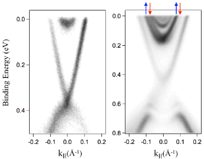
The existence (or not) of Rashba spin-split states at the surface of BSTS is of importance for the magnetoconductance – and in particular – the WAL behaviour. The alpha value we extract for BSTS of close to -1 (Table 2) suggests there is not a contribution from Rashba spin-split states in our BSTS crystals. In Bi2Se3 it is well established from ARPES that topologically trivial, confined bulk states can form a 2DEG in the near surface region and that these states can also show Rashba-type spin splitting [30, 31]. Thus, in Figure 6 we show two ARPES images of the portion of -space near the Gamma-point: one for Bi2Se3 and one for a BSTS crystal from the same source and of the same composition as the flake used for the WAL studies. In both cases, we show ARPES data from surfaces after significant exposure to adsorbates - i.e. for the case of essentially maximal band-bending. The Bi2Se3 data show clear signs of confinement of states related to both the conduction and valence bands, as well as of emerging Rashba-type spin splitting for the states crossing the Fermi level, in accordance with the literature [30, 31]. The left panel of Figure 6 shows analogous data for adsorbate exposed BSTS. The downward band bending has led to the population of states derived from the bulk conduction band, but there is clearly no Rashba-type spin splitting at the BSTS surface. This is fully consistent with the alpha value close to -1 extracted from the analysis of the WAL data shown in Figure 5 and Table 2.
5 Summary
We have presented an extensive study of the bulk-insulating properties of BSTS single crystals. We have synthesized numerous Bi2-xSbxTe3-ySey single crystals with compositions around and , with steps in of 0.02 and of 0.1. The samples were investigated by resistance and Hall effect measurements. We show that via variation of the composition on a fine level, we could arrive at a record-high resistivity, bulk-insulating transport behaviour and a low carrier density, e.g. for multiple growth runs for the composition Bi1.46Sb0.54Te1.7Se1.3. Because of the genuine bulk insulating behavior of these optimized BSTS crystals, the -values obtained at low temperatures are not true resistivity values but depend on the thickness when mm. An analysis of the resistance vs. thickness within a parallel resistor model of the resistance measured for crystals with different thicknesses shows that the surface contribution to the electrical transport amounts to 97 % when the sample thickness is reduced to m. Hence we conclude that devices fabricated with submicrometer thickness are sufficiently bulk insulating to exploit the topological surface states by transport techniques. This conclusion is supported by the observed collapse of the magnetoconductance data of an exfoliated BSTS nanoflake as a function of the perpendicular magnetic field component, further confirming 2D transport. The analysis within the HLN model for 2D weak antilocalization shows the fit parameter as expected for conduction via a pair of topological surface states. Both this fact and our ARPES data recorded under band-bent conditions show a lack of Rashba-split non-topological surface states in our Bi1.46Sb0.54Te1.7Se1.3 crystals.
References
References
- [1] Ren Z, Taskin A A, Sasaki S, Segawa K and Ando Y 2011 Phys. Rev. B 84 165311
- [2] Hasan M Z and Kane C L 2010 Rev. Mod. Phys. 82 3045
- [3] Qi X L and Zhang S C 2011 Rev. Mod. Phys. 83 1057
- [4] Žutić I, Fabian J and Sarma S 2004 Rev. Mod. Phys. 76 323
- [5] Qi X L, Hughes T L, Raghu S and Zhang S C 2009 Phys. Rev. Lett. 102 187001
- [6] Nayak C, Stern A, Freedman M and Das Sarma S 2008 Rev. Mod. Phys. 80 1083
- [7] Hsieh D, Qian D, Wray L, Xia Y, Hor Y S, Cava R J and Hasan M Z 2008 Nature 452 970
- [8] Xia Y, Qian D, Hsieh D, Wray L, Pal A, Bansil A, Grauer D, Hor Y S, Cava R J and Hasan M Z 2009 Nature Phys. 5 398
- [9] Chen Y L, Analytis J G, Chu J H, Liu Z K, Mo S K, Qi X L, Zhang H J, Lu D H, Dai X, Fang Z, Zhang S C, Fisher I R, Hussain Z and Shen Z X 2009 Science 325 178
- [10] Hsieh D, Xia Y, Qian D, Wray L, Meier F, Dil J H, Osterwalder J, Patthey L, Fedorov A V, Lin H, Bansil A, Grauer D, Hor Y S, Cava R J and Hasan M Z 2009 Phys. Rev. Lett. 103 146401
- [11] Roushan P, Seo J, Parker C V, Hor Y S, Hsieh D, Qian D, Richardella A, Hasan M Z, Cava R J and Yazdani A 2009 Nature 460 1106
- [12] Alpichshev Z, Analytis J G, Chu J H, Fisher I R, Chen Y L, Shen Z X, Fang A and Kapitulnik A 2010 Phys. Rev. Lett. 104 016401
- [13] Analytis J G, McDonald R D, Riggs S C, Chu J H, Boebinger G S and Fisher I R 2010 Nat. Phys. 6 960
- [14] Hor Y S, Richardella A, Roushan P, Xia Y, Checkelsky J G, Yazdani A, Hasan M Z, Ong N P and Cava R J 2009 Phys. Rev. B 79 195208
- [15] Chen J, Qin H J, Yang F, Liu J, Guan T, Qu F M, Zhang G H, Shi J R, Xie X C, Yang C L, Wu K H, Li Y Q and Lu L 2010 Phys. Rev. Lett. 105 176602
- [16] Checkelsky J G, Hor Y S, Cava R J and Ong N P 2011 Phys. Rev. Lett. 106 196801
- [17] Ren Z, Taskin A A, Sasaki S, Segawa K and Ando Y 2010 Phys. Rev. B 82 241306(R)
- [18] Xiong J, Luo Y, Khoo Y H, Jia S, Cava R J and Ong N P 2012 Phys. Rev. B 86 045314
- [19] Jia S, Ji H, Climent-Pascual E, Fuccillo M K, Charles M E, Xiong J, Ong N P and Cava R J 2011 Phys. Rev. B 84 235206
- [20] Jia S, Beidenkopf H, Drozdov I, Fuccillo M K, Seo J, Xiong J, Ong N P, Yazdani A and Cava R J 2012 Phys. Rev. B 86 165119
- [21] Ren Z, Taskin A A, Sasaki S, Segawa K and Ando Y 2012 Phys. Rev. B 85 155301
- [22] Fuccillo M, Jia S, Charles M and Cava R 2013 J. Electr. Mater. 42 1246
- [23] Taskin A A, Ren Z, Sasaki S, Segawa K and Ando Y 2011 Phys. Rev. Lett. 107 016801
- [24] Arakane T, Sato T, Souma S, Kosaka K, Nakyama N, Komatsu M, Takahashi T, Ren Z, Segawa K and Ando Y 2012 Nat. Commun. 3 636
- [25] Tang C S, Xia B, Zou X, Chen S, Ou H W, Wang L, Rusydi A, Zhu J X and Chia E E M 2013 Scientific Reports 3 3513
- [26] Ko W, Jeon I, Kim H W, Kwon H, Kahng S J, Park J, Kim J S, Hwang S W and Suh H 2013 Scientific Reports 3 2656
- [27] Kim S, Yoshizawa S, Ishida Y, Eto K, Segawa K, Ando Y, Shin S and Komori F 2014 Phys. Rev. Lett. 112 136802
- [28] Hikami S, Larkin A I and Nagaoka Y 1980 Prog. Theor. Phys. Rev. 63 707
- [29] Lu H Z and Shen S Q 2011 Phys. Rev. B 84 125138
- [30] King P D C, Hatch R C, Bianchi M, Ovsyannikov R, Lupulescu C, Landolt G, Slomski B, Dil J H, Guan D, Mi J L, Rienks E D L, Fink J, Lindblad A, Svensson S, Bao S, Balakrishnan G, Iversen B B, Osterwalder J, Eberhardt W, Baumberger F and Hofmann P 2011 Phys. Rev. Lett. 107 096802
- [31] Bahramy M S, King P D C, de la Torre A, Chang J, Shi M, Patthey L, Balakrishnan G, Hofmann P, Arita R, Nagaosa N and Baumberger F 2012 Nature Commun. 3 1159
- [32] Xia B, Ren P, Sulaev A, Liu P, Shen S Q and Wang L 2013 Phys. Rev. B 87 085442
- [33] Kim D J, Xia J and Fisk Z 2014 Nature Materials 13 466
- [34] Syers P, Kim D, Fuhrer M S and Paglione J 2014 (Preprint 1408.3402)
- [35] Culcer D 2012 Physica E 44 860
- [36] Lu H Z and Shen S Q 2014 Phys. Rev. Lett. 112 146601
- [37] Hsiung T S, Chen D Y, Zhao L, Lin Y H, Mou C Y, Lee T K, Wu M K and Chen Y Y 2013 Appl. Phys. Lett. 103 163111
- [38] Lee J, Park J, Lee J H, Kim J S and Lee H J 2012 Phys. Rev. B 86 245321