Silicon Sensors for Trackers at High-Luminosity Environment
Abstract
The planned upgrade of the LHC accelerator at CERN, namely the high luminosity (HL) phase of the LHC (HL-LHC foreseen for 2023), will result in a more intense radiation environment than the present tracking system was designed for. The required upgrade of the all-silicon central trackers at the ALICE, ATLAS, CMS and LHCb experiments will include higher granularity and radiation hard sensors. The radiation hardness of the new sensors must be roughly an order of magnitude higher than in the current LHC detectors. To address this, a massive RD program is underway within the CERN RD50 collaboration ”Development of Radiation Hard Semiconductor Devices for Very High Luminosity Colliders” to develop silicon sensors with sufficient radiation tolerance. Research topics include the improvement of the intrinsic radiation tolerance of the sensor material and novel detector designs with benefits like reduced trapping probability (thinned and 3D sensors), maximized sensitive area (active edge sensors) and enhanced charge carrier generation (sensors with intrinsic gain). A review of the recent results from both measurements and TCAD simulations of several detector technologies and silicon materials at radiation levels expected for HL-LHC will be presented.
keywords:
Radiation damage; Silicon particle detectors; Radiation hardness; Defect engineering; Detector simulations; HL-LHC1 Introduction
Position sensitive silicon detectors are largely employed in the tracking systems of High Energy Physics experiments due to their outstanding performance. They are currently installed in the vertex and tracking part of the ALICE, ATLAS, CMS and LHCb experiments at LHC, the world’s largest particle physics accelerator at CERN.
An upgrade of LHC accelerator is already planned for 2023, namely the high luminosity phase of the LHC (HL-LHC). Approximately a 10-fold increase of the luminosity will enable the use of maximal physics potential of the machine. After 10 years of operation, the integrated luminosity of 3000 fb-1 [1, 2, 3] will expose the tracking system at HL-LHC to a radiation environment that is beyond the capability of the present system design. At ATLAS and CMS fluences of more than cm-2 (1 MeV neutron equivalent) are expected for the pixel detectors at the innermost layers and fluences above cm-2 for the strip sensors 20 cm from vertex [4]. Besides these extremely high radiation levels the increase in the track density will be among the most demanding challenges. Detectors with finer granularity are therefore required. This means e.g. that the pixel detectors will have to cover the tracking volume to higher radii moving the microstrip detector system further outward. The increased granularity will call for more cost effective technologies than presently existing since otherwise a detector upgrade could not be afforded.
This requires a dedicated RD program to find solutions that improve the present detector technologies, or develop novel ones, for the innermost tracking layers and for replacements for most of the outer detector components with detectors that can withstand higher radiation levels and higher occupancies.
The RD50 collaboration ”Development of Radiation Hard Semiconductor Devices for Very High Luminosity Colliders” [5] was formed in 2002 with the aim to develop semiconductor sensors matching the above mentioned HL-LHC requirements. About 280 members from 50 institutes and of several experiments at the LHC are pursuing this aim in specific research fields, namely defect/material characterization, detector characterization, new structures and full detector systems. The collaboration arranges common sensor production runs, biannual workshops and access to irradiation facilities. These efforts are now closely linked to the increasing upgrade activities of ATLAS and CMS as the RD50 results are already setting some baseline detector concepts for the upgrade.
2 Defect and Material Characterization
The main objective of the research field is the identification of the key radiation effects that adversely affect the sensor properties. Various techniques used for the defect analysis include thermally stimulated current technique (TSC), deep level transient spectroscopy (DLTS), transient current technique (TCT [7]) or capacitance and leakage current measurements versus depletion voltage, (C-V) and (I-V), respectively. The defects are characterized by their capture cross section, ionization energy, concentration and type.
The three radiation effects on the sensor bulk material are the increase of the leakage current, the trapping of charge carriers and the change of the effective doping concentration of the sensor and thus, the depletion voltage.
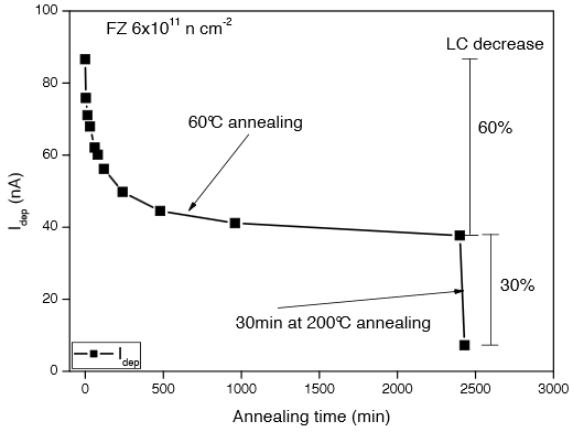
The radiation-induced current increase is proportional to the particle fluence when normalised to the damage generated by neutrons with 1 MeV energy according to the Non Ionising Energy Loss (NIEL) model [8]. On the other hand, the leakage current decreases after annealing and higher annealing temperatures result in further reduction, as shown in figure 1. DLTS measurements attribute this to the defects E4/E5 and E205a [9], where the E denotes an electron trap having a donor level in the bandgap and the number 205 is the observed temperature dependence of the defect in the DLTS spectrum.
The trapping of the drifting signal charges in the silicon bulk effectively reduces the charge collection efficiency (CCE) of the sensor.
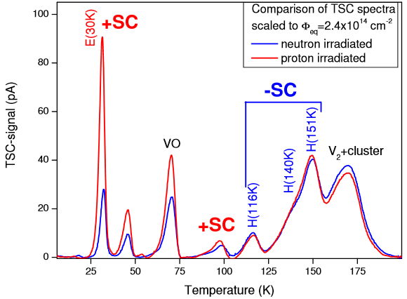
The change of the effective doping concentration proceeds in general through the processes of donor removal and acceptor generation. Typically it has been observed as the device becoming more and more p-type, i.e. a p-type sensor would stay p-type with an increasing , and a n-type sensor would additionally undergo an initial type inversion from n to p. However, measurements of radiation effects on the effective doping concentration in oxygen-enriched n-type epitaxial silicon show a strong dependence on the particle type [11], demonstrating a significant difference between the results from 23 GeV proton and 1 MeV neutron irradiations, thus violating the simple NIEL scaling hypothesis. It is evident in the TSC spectra presented in figure 2 that the proton irradiation produces a much higher concentration of the E(30K) defect compared to the neutron irradiation. Differences for the other defects are much less significant. The E(30K) defect has a donor level in the upper part of the band gap, and it generates a positive space charge (SC) in the silicon bulk. extracted from the C-V measurements confirms that increased donor concentration in proton irradiated samples prevents the type inversion, while the acceptor-like states dominating in neutron irradiated samples lead to the type inversion before the fluence of cm-2 [12].
Also electrons in the energy range of 1.5 - 27 MeV have been observed to generate significant concentrations of E(30K) defects with an introduction rate three times larger in the oxygen-enriched silicon material [6, 13]. The origin of the different radiation effects between particles is not yet fully understood, and constitutes an area of ongoing investigation.
Hence, in the standard n-type (p-type) float zone Si the type inversion occurs (no type inversion occur) irrespective to the type or energy of the radiation, but in the exotic materials like the oxygen-rich Epi-Si the generation of the defects in the band gap depends on the incident particle energy and type. Information of the defects is used for device engineering and as an input to the simulations.
3 Device Simulations
The information of the defects discussed in the previous section is used as an input to the device simulations. The objective is to develop an approach to model and predict the performance of the irradiated silicon detectors (diode, strip, pixel, 3D) using professional software. Simulations are essential in the e.g. device structure optimization or in predicting the electric fields and trapping in the silicon sensors.
The simulation of radiation damage in the silicon bulk is based on the effective mid gap levels (a deep acceptor and a deep donor level with activation energies = - (0.525 0.025) eV and + 0.48 eV, respectively). The model was first proposed in 2001 and entitled later as the ”PTI model” [14]. The main idea of the model is that the two peaks in the E() profile of the both proton and neutron irradiated detectors can be explained via the interaction of the carriers from the bulk generated current with the electron traps and simultaneously with the hole traps. The physical meaning behind all later models is the same combination of the hole and electron traps.
The first successfully developed quantitative models, namely the proton model and the neutron model [15], for the simulation of the detector characteristics like , and the charge collection efficiency (CCE), presented in figure 3, was built on the base of the PTI model with the same two deep levels as those used for the double peak E() explanation.
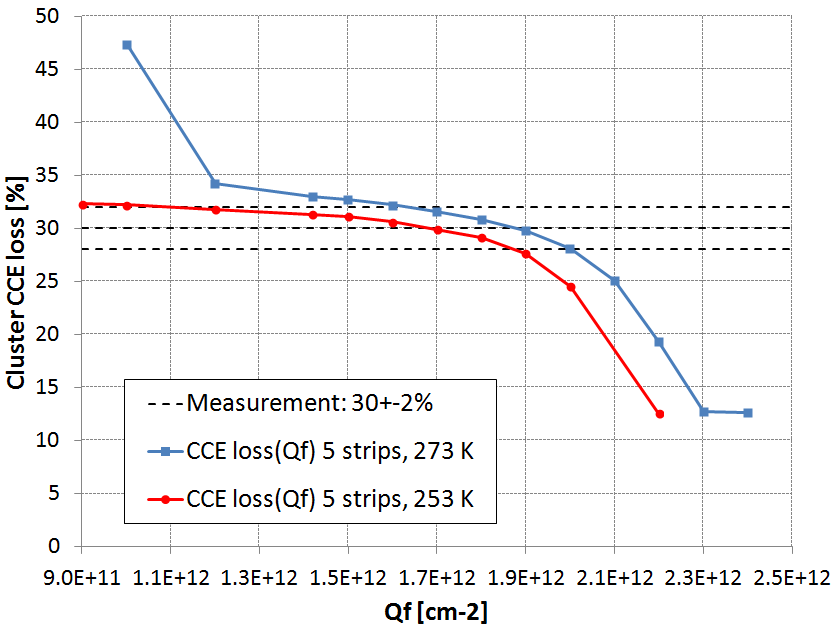
The recent implementations of additional traps at the SiO2/Si interface or close to it have expanded the scope of the simulations to include experimentally agreeing surface properties such as the interstrip resistance and capacitance, and the position dependency of CCE, shown in figure 4, of the strip sensors irradiated up to cm-2 [16, 18, 19, 20, 21]. Currently a common database with the cross sections and concentrations is in preparation and more tuning to the data is ongoing.
4 Detector Characterization
4.1 Detectors on p-type silicon
The planar p-type (or n-in-p) detectors have been brought forward by the RD50 collaboration. They are currently the baseline for the upgrade of the silicon strip tracking detectors at the ATLAS and CMS experiments. The n-in-p sensors have a superior performance resulting from a favourable combination of the weighting and electric fields after irradiation due to the absence of type inversion, and the readout at n-type electrodes, enabling the collection of electrons that have three times higher mobility and longer trapping times than holes. Further essential benefit of the p-type strip sensors is the independence of the CCE of the reverse annealing of the effective space charge in highly irradiated detectors [22, 23, 24].
4.2 Float zone and MCz detectors
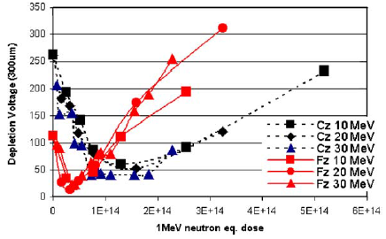
To improve the radiation tolerance of the p-type detectors, both float zone (FZ) and magnetic Czochralski (MCz) sensors have been investigated. CZ and MCz substrates have, due to their specific growth technique, much higher (about cm-3) oxygen content than the FZ and even the Diffusion Oxygenated FZ (DOFZ) silicon [27]. After being introduced by the RD50 collaboration, it is now one of the most important materials for the detector processing.
Measurements have revealed several advantages in the application of the MCz or Cz substrates. Presented in figure 5 the type inversion in the n-type Cz-Si has not occurred before cm-2 fluence. Furthermore, the full depletion voltage in Cz-Si has not exceeded its initial value even after the fluence of cm-2 that equals about 5 years of HL-LHC operation for the strip detectors closest to the vertex [28, 29]. Also the results for the 200 thick FZ and MCz p-type sensors after mixed irradiation to cm-2 give a higher collected charge for the MCz sensors [30]. The MCz sensors are less affected by the annealing and show a stable annealing behaviour. Also an improved performance in mixed fields due to the compensation of neutron and charged particle damage in MCz has been observed [31].
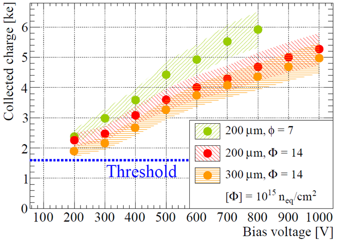
4.3 Thin detectors
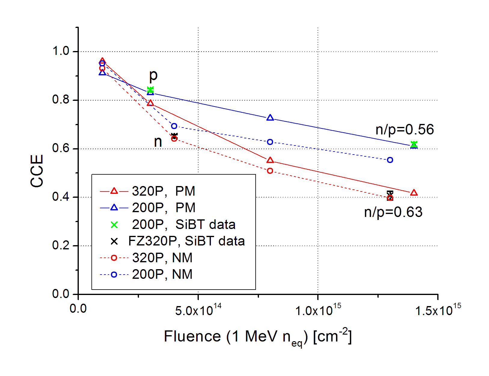
Benefits of the thin detectors are based on reduced mass and, due to the lower trapping probability, some possible advantage in charge collection and reverse current after high irradiation fluences. While the smaller sensitive volume reduces the signal at low fluences, after high fluences of hadron irradiation and operated above the thin detectors could yield a higher signal than thick detectors that cannot reach full depletion because of the high value of [31]. Presented in figure 6 are the collected charges in the 200 and 300 sensors after extremely high proton fluences.
5 New Structures
The investigations of new structures cover, besides the above discussed thin detectors, a variety of new devices like the different types of 3D detectors, sensors with intrinsic gain and slim or active edge sensors.
5.1 3D Detectors
The 3D detectors are likely to be the most promising choice for the extremely high fluence environments. By having doped columns etched into the silicon bulk vertically to the device surface, the geometry of the 3D sensors decouples the depletion voltage and the detector thickness. This means that also the charge drift length is decoupled from the ionization path, i.e. the drift length is now the inter-column spacing, while the signal is still proportional to the detector thickness resulting in a higher radiation tolerance [33].
The downside of the 3D sensors is a more complex processing, a higher inter-electrode capacitance (with higher electronics noise), non-sensitive regions in the columns and the hit position dependent signal size. The disadvantage of the low-field regions is overcome by the 3D trench electrode detectors that have a concentric trench electrode surrounding the central hexagonal signal collecting column electrode [34, 35]. The hexagonal electrode design results in an uniform electric field.
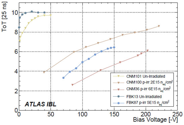
In addition to the single column type [36], also a double column-double sided technology has been developed by the RD50 institutes [37]. Due to being available in large production and being able to give an acceptable signal after irradiation to fluences of , the 3D sensors now populate 25 of the ATLAS experiment insertable b-layer (IBL) [38].
Presented in figure 7 is a study of charge collection in the irradiated FBK222Fondazione Bruno Kessler, www.fbk.eu and CNM333Centro Nacional de Microelectrónica, www.cnm.es produced 3D modules. Since the expected maximum fluence at the IBL is , the results indicate that operation at 160 V is needed for an acceptable charge collection efficiency after irradiation [39].
5.2 Active and slim edge detectors
Reduced edge width is a method used to maximize the sensitive region of the silicon sensors in the tracking detectors. The first edgeless detectors using a break-through junction and operated at low (130 K) were studied in [40]. Later a new construction was proposed based on the optimization of the electric field distribution on the edge and its control by the amorphisation of the edge surface [41] making useless the voltage termination structure between the edge and the detector active area. This structure can be totally replaced by a single ring which controls the current distribution between the edge and the sensitive volume. This entirely solves the problem with the edgeless detector premature breakdown in detectors with a very narrow 45 non-sensitive contour at the edge. On the basis of this principle 240 microstrip detectors out of 400 processed were installed and successfully operated at the TOTEM experiment during the first two-year long run of the LHC.
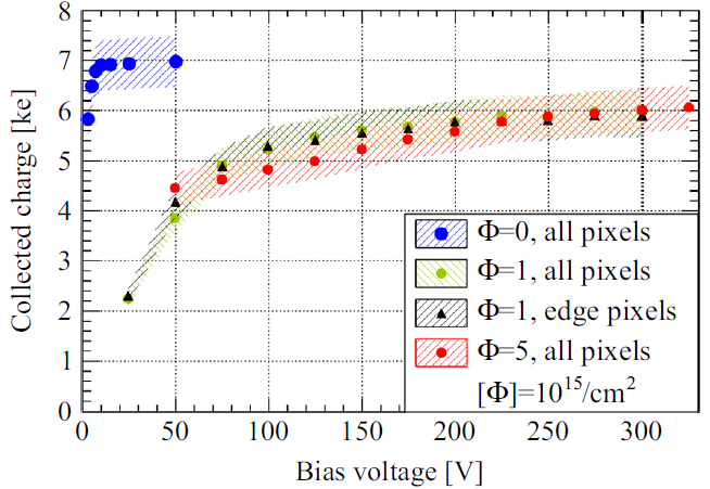
Further approaches have since been developed to minimize the non-active volume, resulting in slim and active edge sensors. The scribe-cleave-passivate technology aims to reach 100 or less slim edges, while the typical distances to the edge are in the range 500-1000 [42]. Alternatively, pixel sensors with active edges are manufactured by wet etching trenches at the sensor border that are then activated by the means of four-quadrant ion implantations [43]. Presented in figure 8 are the charge collection measurements of the thin p-type pixel sensors with 125 width active edges (processed using the last mentioned method at VTT444VTT Technical Research Centre of Finland Ltd., http://www.vtt.fi) before and after irradiation. Similar median charge for the strips close to the edge and other strips are collected.
5.3 Sensors with intrinsic gain
The effect of the charge multiplication has been observed in several device types, namely the strip sensors, 3D sensors and diodes [44, 45, 46]. The enhancement arises from the carrier avalanche multiplication in the high electric field of the junction, resulting from a high negative space charge concentration in the bulk after irradiation [47].
Extensive modelling of the detectors with intrinsic gain has already been carried out [48, 47] and a dedicated program has been setup within the RD50 collaboration to understand the underlying mechanisms of the multiplication, to simulate them and to optimize the CCE performances.
To this end special charge multiplication sensors have been fabricated. The newly developed sensors with intrinsic gain, i.e. Low Gain Avalanche Detectors (LGAD), are based on avalache photodiode technology and feature an implemented multiplication layer, a deep p+ implant below the cathodes. An edge termination done by a low doping n-well is needed to secure gain uniformity [49].
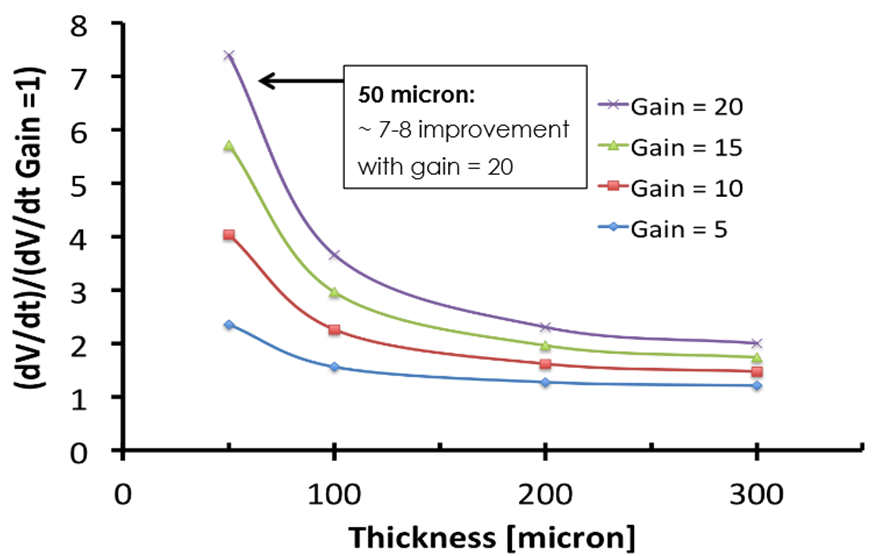
Gain values of up to 20 for 90Sr electrons have been measured [50] in the non-irradiated LGADs while the leakage current and noise are independent of the gain [51]. With this technology thinner detectors can be produced to give the signal of thick ones, enabling the investigation of ultra-fast detectors [52, 53] for HL-LHC. The dependence of the time resolution on gain and device thickness is presented in figure 9.
After irradiation a significant reduction in gain is occuring. Neutron irradiation to a fluence of leads to a signal that is compatible with a standard diode and for 800 MeV protons of fluence almost no gain can be observed. Instead of trapping the effective acceptor removal in the p+ layer is responsible for the gain degradation by reducing the electric field [50]. Presently more wafers are in production for further tests and an irradiation programme has been planned.
6 Summary
An overview of the RD50 collaboration research activities for developing sensors with sufficient radiation hardness for the HL-LHC has been given including several examples of the work performed by the RD50 collaboration.
Defect characterization results indicate that in the standard n-type (p-type) float zone Si the type inversion occurs (no type inversion occur) irrespective to the type or energy of radiation, but in more exotic materials like the oxygen-rich Epi-Si the generation of the defects in the band gap depends on the incident particle energy and type.
TCAD simulations carried out by a dedicated work group are now able to account for both bulk and surface damage resulting in further convergence with the measurements and increasing predictive power.
The sensors with n-electrode readout (mainly sensors with p-bulk) offer the advantage of collecting electrons instead of holes resulting in an improvement of radiation tolerance. For the outer layer with maximum fluences of about planar n-in-p sensors are the baseline for the ATLAS and CMS upgrade strip tracker. MCz was shown to be more radiation tolerant than the standard FZ silicon with respect to the change of the effective doping concentration. Furthermore, it has been observed that in the n-MCz material neutron and proton irradiations introduce effects that act as doping of opposite polarity, leading to a possible partial cancellation effect of the degradation of . The thin detectors overcome the requirement of high bias voltages and are advantageous at fluences above .
The 3D detectors are a promising option and show good performance requiring lower bias voltages. The designs include now the single column type, the double column-double sided type and the trench electrode detectors. Due to being able to give an acceptable signal after irradiation to , the 3D sensors now populate 25 of the ATLAS IBL. The edgeless, active or slim edge devices have been developed to maximize the sensitive region of the silicon sensors in tracking detectors. 240 edgeless microstrip detectors were already installed and successfully operated at the TOTEM experiment during the first two-year long run of LHC. The effect of the charge multiplication is investigated systematically to allow its exploitation and dedicated sensors have been produced. The sensors with intrinsic gain offer the possibility for the thin detectors to produce the signal of thick ones, enabling the investigation of ultra-fast planar detectors for HL-LHC. This requires first a solution to the significant reduction of gain after irradiations at expected fluences.
For further results aiming for radiation hard semiconductor devices for the future colliders, the website of the RD50 collaboration is referred.
Acknowledgement
The author would like to thank the colleagues of the RD50 Collaboration for the material and support.
References
- [1] L. Rossi, O. Brüning, High Luminosity Large Hadron Collider - A description for the European Strategy Preparatory Group, CERN-ATS-2012-236 (2012).
-
[2]
LHC Project Report 626, in:
F. Ruggiero (Ed.), LHC Luminosity and Energy Upgrade: A Feasibility
Study, CERN, 2002.
URL {http://cern.ch/lhc-proj-IR-upgrade/} - [3] F. Gianotti, et al., Physics potential and experimental challenges of the LHC luminosity upgrade, hep-ph/0204087 (April 2002).
- [4] I. Dawson, Radiation predictions at the SLHC and irradiation facilities, ATLAS Tracker Upgrade Workshop, Liverpool, UK, 2006.
- [5] The RD50 collaboration, http://cern.ch/rd50/.
- [6] RD50 Status Report 2009/2010, CERN-LHCC-2012-010, LHCC-SR-004 (available on Ref. [5]).
- [7] V. Eremin, N. Strokan, E. Verbitskaya, Z. Li, Development of transient current and charge techniques for the measurement of effective net concentration of ionized charges () in the space charge region of p-n junction detectors, Nucl. Instr. Meth. A 372 (1996) 388–398. doi:10.1016/0168-9002(95)01295-8.
- [8] M. Huhtinen, Simulation of non-ionising energy loss and defect formation in silicon, Nucl. Instr. Meth. A 491 (2002) 194–215. doi:10.1016/S0168-9002(02)01227-5.
-
[9]
A. Junkes, Status of defect investigations, in: Proceedings of
Science, 2011, PoS(Vertex 2011)035.
URL http://pos.sissa.it/archive/conferences/137/035/Vertex2011_035.pdf - [10] A. Junkes, Influence of Radiation Induced Defect Clusters on Silicon Particle Detectors, Ph.D. thesis, Universität Hamburg, DESY-THESIS-2011-031 (July 2011).
- [11] I. Pintilie, et al., Radiation-induced point- and cluster-related defects with strong impact on damage properties of silicon detectors, Nucl. Instr. Meth. A 611 (2009) 52–68. doi:10.1016/j.nima.2009.09.065.
- [12] U. Parzefall, Silicon for High-Luminosity Tracking Detectors - Recent RD50 Results, Physics Procedia 37 (2012) 899–906.
- [13] R. Radu, et al., Investigation of point and extended defects in electron irradiated silicon - dependence on the particle energy, Bucharest, 2014, 24th RD50 Workshop.
- [14] V. Eremin, E. Verbitskaya, A. Zabrodskii, Z. Li, J. Härkönen, Avalanche effect in Si heavily irradiated detectors: physical model and perspectives for application., Nucl. Instr. Meth. A 658 (2011) 145–151. doi:10.1016/j.nima.2011.05.002.
-
[15]
R. Eber,
Investigations of new Sensor Designs and Development of an
effective Radiation Damage Model for the Simulation of highly
irradiated Silicon Particle Detectors, Ph.D. thesis, Karlsruhe
Institute of Technology (2013).
URL http://ekp-invenio.physik.uni-karlsruhe.de/record/48328%/files/EKP-2014-00012.pdf -
[16]
T. Peltola,
Charge Collection Efficiency Simulations of Irradiated Silicon
Strip Detectors, JINST, CMS CR-2014/255.
URL {http://cds.cern.ch/record/1954727/files/CR2014_255.pdf%%****␣RD50resmdd14.bbl␣Line␣100␣****?version=1} - [17] J. Härkönen, et al., Test beam results of a heavily irradiated Current Injected Detector (CID), Nucl. Instr. Meth. A 612 (2010) 488–492. doi:10.1016/j.nima.2009.08.006.
-
[18]
T. Peltola, et al.,
A Method to
Simulate the Observed Surface Properties of Proton Irradiated
Silicon Strip Sensors, JINST, CMS CR-2014/247.
URL {http://cds.cern.ch/record/1956767/files/CR2014_247.pdf%} - [19] Silicon Sensor Simulation Working Group, Simulation of Silicon Devices for the CMS Phase II Tracker Upgrade, CMS DN-2014/016 (2014).
-
[20]
R. Dalal, et al.,
Development
of Radiation Damage Models for Irradiated Silicon Sensors Using
TCAD Tools, JINST, CMS CR-2014/120.
URL {http://cds.cern.ch/record/1712501/files/CR2014_120.pdf%} -
[21]
T. Eichhorn, et al.,
Simulations
of Inter-Strip Capacitance and Resistance for the Design of the
CMS Tracker Upgrade, JINST, CMS CR-2014/126.
URL {http://cds.cern.ch/record/1712499/files/CR2014_126.pdf%} - [22] G. Casse, et al., First results on the charge collection properties of segmented detectors made with p-type bulk silicon, Nucl. Instr. Meth. A 487 (2002) 465–470. doi:10.1016/S0168-9002(02)00263-2.
- [23] G. Casse, P. P. Allport, A. Watson, Effects of accelerated annealing on p-type silicon micro-strip detectors after very high doses of proton irradiation, Nucl. Instr. Meth. A 568 (2006) 46–50. doi:10.1016/j.nima.2006.05.200.
- [24] G. Kramberger, V. Cindro, I. Mandić, M. Mikuž, M. Zavrtanik, Effective trapping time of electrons and holes in different silicon materials irradiated with neutrons, protons and pions, Nucl. Instr. Meth. A 481 (2002) 297–305. doi:10.1016/S0168-9002(01)01263-3.
- [25] G. Casse, P. P. Allport, S. M. i Garcia, M. Lozano, P. Turner, Performances of miniature microstrip detectors made on oxygen enriched p-type substrates after very high proton irradiation, Nucl. Instr. Meth. A 535 (2004) 362–365. doi:10.1016/j.nima.2004.07.153.
- [26] M. Moll, Radiation tolerant semiconductor sensors for tracking detectors, Nucl. Instr. Meth. A 565 (2006) 202–211. doi:10.1016/j.nima.2006.05.001.
- [27] A. Barcz, M. Zielinski, E. Nossarzewska, G. Lindström, Extremely deep SIMS profiling: oxygen in FZ silicon, Appl. Surf. Sci. 203-204 (2003) 396–399. doi:10.1016/S0169-4332(02)00687-6.
- [28] J. Härkönen, et al., Processing of microstrip detectors on Czochralski grown high resistivity silicon substrates, Nucl. Instr. Meth. A 514 (2003) 173–179. doi:10.1016/j.nima.2003.08.102.
- [29] J. Härkönen, et al., Particle detectors made of high resistivity Czochralski silicon, Nucl. Instr. Meth. A 541 (2005) 202–207. doi:10.1016/j.nima.2005.01.057.
- [30] G. Steinbrück, Radiation hard silicon sensors for the CMS tracker upgrade, presented at the 23rd RD50 Workshop (Nov. 2013).
- [31] G. Casse, Overview of the recent activities of the RD50 collaboration on radiation hardening of semiconductor detectors for the sLHC, Nucl. Instr. Meth. A 598 (2009) 54–60. doi:10.1016/j.nima.2008.08.019.
-
[32]
S. Terzo, A. Macchiolo, R. Nisius, B. Paschen,
Thin n-in-p planar pixel sensors
and active edge sensors for the ATLAS upgrade at HL-LHC, JINST, to be
published.
URL {http://arxiv.org/abs/1409.8579} - [33] S. I. Parker, C. J. Kenney, J. Segal, 3D - A proposed new architecture for solid-state radiation detectors, Nucl. Instr. Meth. A 395 (1997) 328–343. doi:10.1016/S0168-9002(97)00694-3.
- [34] Z. Li, New BNL 3D-Trench electrode Si detectors for radiation hard detectors for sLHC and for X-ray applications, Nucl. Instr. Meth. A 658 (2011) 90–97. doi:10.1016/j.nima.2011.05.003.
- [35] A. Montalbano, et al., A systematic study of BNL’s 3D-Trench Electrode detectors, Nucl. Instr. Meth. A 765 (2014) 23–28. doi:10.1016/j.nima.2014.03.066.
- [36] C.Piemonte, et al., Development of 3D detectors featuring columnar electrodes of the same doping type, Nucl. Instr. Meth. A 541 (2005) 441–448. doi:10.1016/j.nima.2005.01.087.
- [37] G. Pellegrini, et al., First double-sided 3-D detectors fabricated at CNM-IMB, Nucl. Instr. Meth. A 592 (2008) 38–43. doi:10.1016/j.nima.2008.03.119.
- [38] ATLAS collaboration, ATLAS Insertable B-layer Technical Design Report, http://cds.cern.ch/record/1291633/files/ATLAS-TDR-019.pdf?version=2, CERN-LHCC-2010-013 (2010).
- [39] The ATLAS IBL collaboration, Prototype ATLAS IBL modules using the FE-I4A front-end readout chip, JINST 7 (P11010). doi:10.1088/1748-0221/7/11/P11010.
- [40] Z. Li, et al., Electrical and TCT characterization of edgeless Si detector diced with different methods, IEEE Trans. Nucl. Sci NS-49 (2002) 1040–1046. doi:10.1109/NSSMIC.2001.1008441.
- [41] G. Ruggiero, et al., Characteristics of edgeless silicon detectors for the Roman Pots of the TOTEM experiment at the LHC, Nucl. Instr. Meth. A 604 (2009) 242–245. doi:10.1016/j.nima.2009.01.056.
- [42] V. Fadeyev, et al., Scribe-cleave-passivate (SCP) slim edge technology for silicon sensors, Nucl. Instr. Meth. A 731 (2013) 260–265. doi:10.1016/j.nima.2013.03.046.
- [43] A.Macchiolo, et al., Development of active edge pixel sensors and four-side buttable modules using vertical integration technologies, Nucl. Instr. Meth. A 765 (2014) 53–58. doi:10.1016/j.nima.2014.06.073.
- [44] J. Lange, et al., Properties of a radiation-induced charge multiplication region in epitaxial silicon diodes, Nucl. Instr. Meth. A 622 (2010) 49–58. doi:10.1016/j.nima.2010.07.036.
- [45] G. Casse, et al., Enhanced efficiency of segmented silicon detectors of different thicknesses after proton irradiations up to , Nucl. Instr. Meth. A 624 (2010) 401–404. doi:10.1016/j.nima.2010.02.134.
- [46] M. Koehler, et al., Comparative measurements of highly irradiated n-in-p and p-in-n 3D silicon strip detectors, Nucl. Instr. Meth. A 659 (2011) 272–281. doi:10.1016/j.nima.2011.08.041.
- [47] E. Verbitskaya, V. Eremin, A. Zabrodskii, Z. Li, P. Luukka, Restriction on the gain in collected charge due to carrier avalanche multiplication in heavily irradiated Si strip detectors, Nucl. Instr. Meth. A 730 (2013) 66–72. doi:10.1016/j.nima.2013.06.086.
- [48] E. Verbitskaya, V. Eremin, A. Zabrodskii, Operational voltage of silicon heavily irradiated strip detectors utilizing avalanche multiplication effect, JINST 7 (C02061). doi:10.1088/1748-0221/7/02/C02061.
- [49] G. Pellegrini, et al., Technology developments and first measurements of Low Gain Avalanche Detectors (LGAD) for high energy physics applications, Nucl. Instr. Meth. A 765 (2014) 12–16. doi:10.1016/j.nima.2014.06.008.
- [50] G. Kramberger, Radiation hardness of Low Gain Amplification Detectors (LGAD), presented at the 24th RD50 Workshop (June 2014).
- [51] G. Kramberger, Studies of CNM diodes with gain, presented at the 22nd RD50 Workshop (June 2013).
- [52] H. F.-W. Sadrozinski, et al., Ultra-fast silicon detectors, Nucl. Instr. Meth. A 730 (2013) 226–231. doi:10.1016/j.nima.2013.06.033.
- [53] H. F.-W. Sadrozinski, et al., Sensors for ultra-fast silicon detectors, Nucl. Instr. Meth. A 765 (2014) 7–11. doi:10.1016/j.nima.2014.05.006.
- [54] N. Cartiglia, et al., Timing capabilities of Ultra-Fast Silicon Detector, presented at the 24th RD50 Workshop (June 2014).