Very Low Cost Entropy Source Based on Chaotic Dynamics Retrofittable on Networked Devices to Prevent RNG Attacks
Abstract
Good quality entropy sources are indispensable in most modern cryptographic protocols. Unfortunately, many currently deployed networked devices do not include them and may be vulnerable to Random Number Generator (RNG) attacks. Since most of these systems allow firmware upgrades and have serial communication facilities, the potential for retrofitting them with secure hardware-based entropy sources exists. To this aim, very low-cost, robust, easy to deploy solutions are required. Here, a retrofittable, sub 10$ entropy source based on chaotic dynamics is illustrated, capable of a 32 kbit/s rate or more and offering multiple serial communication options including USB, I2C, SPI or USART. Operation is based on a loop built around the Analog to Digital Converter (ADC) hosted on a standard microcontroller.
I Introduction
One of the most powerful trends recently seen in technology is the networking of a large number of devices originally operating in isolation. By 2020 more than 25 billion devices will be interconnected [1]. This Internet of Things (IoT) can bring smartness to many environments whose items gain the ability to cooperate and a richer set of information to base their behaviors upon. At the same time, making a huge number of devices remotely reachable poses profound security challenges because of the immense attack surface [2].
Unfortunately, many devices being brought online lack certain security-oriented subsystems. This is due to cost and conception, since networking is often applied to mundane items and awareness on security issues is still growing. In a short time, there will be a huge legacy of networked devices missing hardware parts critical to security. This can be long lasting since humble devices lack any upgrade lust and are only substituted when they break, as users often fail to see potential threats as lack of functionality. Surveys reveal that about half of the networking devices found in businesses are already on the brink of obsolescence [3]. To contrast this phenomena, some authors suggest that embedded networking units should be given a scheduled end-of-life [4]. Until this is a reality (if ever), the alternative is to minimize the costs of patching current devices, either in manufacturing, through design revisions, or on field, through software upgrades and hardware retrofits.
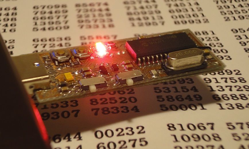
This paper illustrates the design of a hardware primitive critical for security, namely an entropy source, whose absence can favor RNG attacks (references to past incidents in [5]). True-RNGs and hardware entropy sources are becoming mainstream in computers [6], but are still missing from most low-cost/embedded devices. The current proposal can be declined in multiple forms: from a self-contained plug-in applicable on field to existing systems (Fig. 1) to a schematic upgrade re-using an existent microcontroller (μC), targeting manufacturers. In either case, key features are: (i) very low cost (sub-10$ for a self-contained unit with Universal Serial Bus (USB) connector, sub-5$ for designs where a μC is available to share); and (ii) high interconnection flexibility (USB, I2C, SPI or USART interfaces, depending on the adopted μC) in order to favor adoption as a retrofit. The entropy rate that can be delivered is in the few tens kbit/s range, depending on the μC (over 32 kbit/s have been experimentally observed with a PIC18F2550).
Similar solutions are scarce on the market, with true-RNG retrofits ranging from near 40$ to over 1000$ (i.e., at far higher costs, even considering selling margins). Closest competitors are the TRNG98 modules [7], and the Simtec Entropy Key. Differently from any other design, the current proposal is based on chaotic dynamics, rather than direct amplification of electronic noise (thermal, avalanche, etc.), which can make the system less susceptible to tampering and side channel attacks [8]. It is not the first time that chaos is proposed for RNGs [9], but the current design has the distinguished feature of re-using ADCs readily available on μCs. ADC reuse, originally introduced in [10], has already seen experimental validation [8], but so far only on full-custom integrated circuits with ad-hoc designed pipeline ADCs, where stages can be separated from each other. Here, taking advantage of the generalized theory in [11, 12], the approach is used for the first time on an unmodified commercial ADC, with a successive approximation architecture and harsh operating conditions (μC ADCs are often poorly isolated from digital noise). This setup requires some specific design arrangements that are here thoroughly detailed.
II Background: RNGs and security
Cryptographic systems base their operation on the existence of some secret data known to authorized users and unpredictable by others. To warrant unpredictability, random strings are often employed, e.g., in keys, salts, nonces, initialization vectors, challenges, and other one-time quantities. Generating these strings can be non-trivial, since digital system, by nature, cannot behave randomly. Compromises have traditionally been made, using algorithms, known as pseudo-RNGs, capable of expanding short seeds into irregular long sequences. Unfortunately, this has recently lead to security incidents. In fact, discovery of the algorithm state by an attacker provides the ability to predict future ‘random’ quantities [13]. In some cases, RNG attacks had a high impact, pushing big players of information technology to incorporate true-RNGs in their larger and newer systems [6].
For simpler or legacy systems, software solutions have been developed capable of gathering noisy data (entropy) from peripherals ‘perceiving’ physical phenomena complex enough to be assumed random. For instance, many operating systems have access to mouse movements, key press timings, hard disk latencies, etc. Such quantities are irregular, but may show correlations. Yet, they can be accumulated in buffers from which good random numbers can be distilled through operations such as hashing and the frequent re-seeding of pseudo-RNGs [14]. This works fairly well for standard computers, but may fail for little devices in an IoT scenario. In fact, the latter may lack most of the peripherals needed to collect entropy (for instance, little routers, networked thermostats, and so on do not have mouses, keyboards or hard-disks). With this, attempts at entropy distillation may even become counterproductive, giving a false sense of security while in fact falling back to pseudo-RNG behavior due to lack of inputs.
The ultimate fix is clearly to bring true-RNGs even to humble devices. Doing so in the form of hardware retrofits needs carefully weighing the available options. Ultimately, true-RNGs are analog systems that harvest information from physical phenomena so intricated at the microcosmic level to appear random at the macroscopic scale. Their simplest implementation consists in the direct amplification and acquisition of electronic noise (thermal, avalanche, etc). This can be effective but is inherently exposed to tampering, since interference may be easily exchanged from genuine noise, so that (expensive) shields can be mandatory [7]. Another form of amplification is to exploit the meta-stability of positive feedback structures. A further alternative is to deploy phase noise in oscillators that mutually sample each other. This lets the analog quantity be time, so that digital voltage levels can be adopted. Furthermore, susceptibility to tampering is improved by the more indirect harvesting. Finally, at the highest level of sophistication, one finds circuits based on chaotic dynamics.
The chaos-based approach is inherently different from all the others. First of all, chaotic-RNGs replicate at the circuit level some of the features, including sensitivity to initial conditions [15], conjectured to be at the root of randomness in natural systems. Secondly, they harvest noise in a radically different way. Non-chaotic sources need to continuously gather new noise samples, while chaotic source could in principle use just the uncertainty in their start-up condition, thanks to sensitivity to initial conditions. In practice, noise will certainly be present throughout all the operating time, but this ends up being just a bonus, since correct functionality does not strictly demand it. For this reason, as long as it is independent from their inner state, noise or interference collected during operation can often bear only minor influence on output quality (unless it is very large, but in this case tampering can typically be detected with ease).
III ADC based true-RNG
Among all possible chaotic sources, discrete time ones based on the iteration of 1-dimensional Piece-Wise Affine Markov (PWAM) maps [10] are very appealing. The corresponding model is
| (1) |
where an invariant set (here normalized to ) exists for . The PWAM nature of assures that a partition of exists such that the dynamics, once observed through a -induced quantization function , can be modeled through a Markov chain [11].
Shift type maps, such as
| (2) |
with integer are particularly interesting. They assure that any subdivision of in equally sized sub-intervals, wrapped around at the invariant set boundaries, results in a Markov partition regardless of . Namely, the partition can be built taking any and sets for , such that
| (3) |
The corresponding Markov chain has states, with transition probabilities among any two of them equal to . In other words, it is identical to the chain describing the cast of an -faced unbiased die [11]. Thus, the system has the ability to generate random symbols.
Interestingly, shift maps can be easily obtained by deriving the quantization error of an ADC, as shown in Fig. LABEL:sub@sfig:adcdac.
| (a) | |
| (b) | |
| (c) |
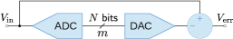
Let and be used to indicate the static characteristics of the ADC and the Digital to Analog Converter (DAC), respectively. For an bit single ended ADC, one should ideally have
| (4) |
where is the reference voltage (approximately equal to the full scale) and a flooring ADC behavior is assumed. Quantization step is . For the complementary bit DAC one has
| (5) |
so that the quantization error, estimated as show in the figure is
| (6) |
The expression already contains the modulus operation that characterizes Eqn. (2). Now, assume that a further block, as shown in Fig. LABEL:sub@sfig:proc computes . Altogether
| (7) |
Rearranging the terms, one has
| (8) |
It is now sufficient to introduce the voltage-to- transformation
| (9) |
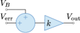
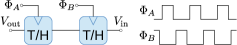
to see that Eqn. (8) defines the map , with and . From this, to obtain a dynamical system such as that in Eqn. (1), it is enough to feed back into through a delay element. The latter can be implemented as the cascade of two Track-and-Holds blocks operating in a master-slave fashion, as in Fig. LABEL:sub@sfig:aregister. With this, while spans , the voltages and span . The situation is illustrated in Fig. 3, from which it is evident that some bounds are needed for the parameters. Specifically, (with ), and , i.e., .
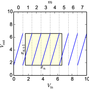
Interestingly, the figure also makes evident that the ADC quantization inherently provides a -state Markov partition for the map. In fact, the range is as wide as , and contains exactly quantization steps. Specifically, it is sufficient to take in order to have intervals such as those in Eqn. (3). This is convenient, since it lets the Markov state be directly readable from the output of the ADC. In detail, one gets that the spanned values fit between
| (10) |
and that system is in state when
| (11) |
With this, one has a true-RNG that randomly picks a value in an alphabet of symbols at each cycle. As an example, Fig. 4 shows the Markov chain corresponding to the setup in Fig. 3. In view of an efficient implementation, it is clearly convenient to make a power of , say with , so that each generated value fits exactly in bits. Clearly, one needs . In principle, should be large so that many random bits can be generated per cycle. Yet, and must often be contained to ease implementation.
IV Practical implementation on a μC
IV-A Implementation principles
Intuitively, the concepts illustrated so far can be easily materialized by a μC based architecture as shown in Fig. 5.
| (a) | |
| (b) |
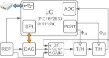
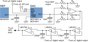
Since most μCs already include an ADC, the number of external components can be very low. The loop corresponding to the model in Eqn. (1) can be closed via an external DAC (for instance, the MPC4901 or MPC4911, communicating with the μC on the SPI bus). The loop gain and offset can be provided by a difference amplifier (for instance, obtained by half an LVM602 or LMV792 chip), controlling and by means of its resistors ( to in the schematic). The loop delay requires two T/H units. These can be obtained by Operational Amplifiers with an output enable feature, followed by suitably large capacitors (for instance each T/H can be obtained by an LVM601). A voltage reference is required for accurate operation. Some μCs readily provide one, otherwise a dedicated chip (such as the MAX6004) can be used. In the proposed architecture, the loop path goes through the μC, which acquires the T/H output and passes the corresponding numerical data to the external DAC via its SPI bus. The μC is also in charge of generating the timing signals for the DAC and the T/H units. These are transferred via 3 lines on one of the digital I/O ports. For prototyping a stand alone unit, the PIC18F2550 μC can conveniently be selected, in view of its low price and integrated USB bus, which favors interfacing. In fact, many little network devices include USB connection facilities. Alternatively, the portion of schematic in Fig. LABEL:sub@sfig:detail can be added to an existing design including a μC with some spare computational resources. With this, costs can be further lowered.
A notable advantage of the proposal is that it makes readily available inside the μC. Consequently, at each cycle, the μC can compute a random symbol from it while passing it to the DAC. The so generated symbols can be progressively accumulated and packed in bytes. When the μC has buffered enough of them (or when a request arrives), they can be transferred to the embedding system via one of the μC communication interfaces, for instance, the USB bus, possibly under encryption to prevent snooping or tampering.
IV-B Implementation requirements
In practice, the implementation cannot be so direct and requires some care. Specifically, it is not possible to straightforwardly deploy the block diagram in Fig. 2, because of implementation uncertainties. For instance, in most μC, the ADC least significant bits can be quite erratic due to couplings with digital lines. Furthermore, accuracy in the setting of should be in the order of half a quantization step, but this is too fine to achieve when the ADC resolution is 8–10 bits. Any implementation attempt ignoring these matters would most certainly fail. Fortunately, the two issues can be easily worked around by artificially degrading the ADC resolution before computing . This can be done as follows. Assume that is the nominal ADC resolution and that is the actual -bit ADC output at each cycle, then let be just a portion of , so that can be obtained by shifting right by bits. With this, the value to be passed to the DAC can be obtained by back shifting to the left with zero padding. Incidentally, this permits the use of an external DACs with a lower resolution , as long as . Good values can be to bits. Furthermore, (which determines ) must be taken to be strictly less than . In fact, this lets be chosen so that the range lies with clearance within the ADC input range and the OA output saturation voltages. Good values are to bits, depending on , while good values let fall halfway between voltages corresponding to transition points for .
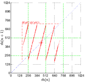
An advantageous side effect of the artificial resolution degradation is that it lets the μC observe the chaotic system state via , i.e., at a resolution higher than the bits required for operation. In other words, one gains insight on the analog system state without the need for external instrumentation. Such an opportunity can be useful in view of self diagnostics or automatic detection of tampering attempts. As an example, Fig. LABEL:sub@sfig:experiment-map shows a reconstruction of the iterated map obtained by actual experimental data acquired by the μC itself.
IV-C Experimental validation
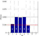
The proposed architecture has been extensively tested, using the prototype illustrated in Fig. 1. For the tests, parameters have been set as in the caption of Fig. 6. Pane LABEL:sub@sfig:probs shows the experimentally obtained values and their relative frequencies. The numbers on the graph columns indicate the output bits associated to each value (obtained as ). Their occurrence probability is well balanced at approximately . Long output streams have been tested for their information content, achieving bits of entropy for each delivered output bit (estimated via a marginal entropy approach). The NIST 800-22 suite [16] has also been applied. The corresponding tables of outcomes cannot fit in this paper, but are worth summarizing. The raw generator is incapable of passing all tests (though it can already pass many of them). Yet, a minimal post-processing (by a Von Neumann corrector or the XORing of consecutive bits) is already sufficient for full conformance. Similarly, when the raw data produced by the generator is used to feed the entropy distiller in the Linux Operating System (OS), the distiller output can pass all tests.
V Conclusions
A new architecture of a μC based true-RNG has been proposed, prototyped and tested. Internally it relies on chaotic dynamics. Expected cost is extremely low and many interconnection options are possible, making it suitable as a retrofit for existing networked units that lack a true-RNG and that may be exposed to RNG attacks.
References
- [1] P. Middleton, P. Kjeldsen, and J. Tully, “Forecast: The internet of things, worldwide, 2013,” Gartner, Report G00259115, Nov. 2013.
- [2] R. Roman, P. Najera, and J. Lopez, “Securing the internet of things,” IEEE Computer, vol. 44, no. 9, p. 51–58, 2011.
- [3] S. Lynn, “Survey: Biz network devices vulnerable, almost obsolete,” PC Magazine (Online), May 2011. [Online]. Available: http://www.pcmag.com/article2/0,2817,2385833,00.asp
- [4] D. Geer, “Security of things,” presented at the Security of Things Forum, Cambridge, MA, USA, May 2014, keynote speech. [Online]. Available: http://geer.tinho.net/geer.secot.7v14.txt
- [5] Wikipedia, “Random number generator attack,” 2014, accessed 2014-05-13. [Online]. Available: http://en.wikipedia.org/wiki/Random_number_generator_attack
- [6] G. Taylor and G. Cox, “Digital randomness,” IEEE Spectr., vol. 48, no. 9, p. 32–58, 2011.
- [7] B. D. Electronics, “TRNG9880 random number processing,” Dec. 2013, white paper. [Online]. Available: www.trng98.se/getfile.php?file=trng9880_info.pdf
- [8] F. Pareschi, G. Scotti, L. Giancane, R. Rovatti, G. Setti, and A. Trifiletti, “Power analysis of a chaos-based random number generator for cryptographic security,” in Proc. IEEE Intern. Symp. on Circuits and Systems, 2009, 2009, pp. 2858–2861.
- [9] S. Callegari, R. Rovatti, and G. Setti, “First direct implementation of true random source on programmable hardware,” International Journal of Circuit Theory and Applications, John Wiley & Sons, vol. 33, no. 1, pp. 1–16, 2005. DOI:10.1002/cta.301
- [10] S. Callegari, R. Rovatti, and G. Setti, “Embeddable ADC-based true random number generator for cryptographic applications exploiting nonlinear signal processing and chaos,” IEEE Trans. Signal Process., vol. 53, no. 2, pp. 793–805, Feb. 2005. DOI:10.1109/TSP.2004.839924
- [11] S. Callegari and G. Setti, “ADCs, chaos and TRNGs: a generalized view exploiting Markov chain lumpability properties,” in Proc. of ISCAS, New Orleans, LA (USA), May 2007, pp. 213–216. DOI:10.1109/ISCAS.2007.378314
- [12] S. Callegari, “Introducing Complex Oscillation Based Test: an application example targeting analog to digital converters,” in Proc. of ISCAS, Seattle, WA (USA), May 2008, pp. 320–323. DOI:10.1109/ISCAS.2008.4541419
- [13] D. E. Eastlake, J. I. Shiller, and S. D. Crocker, “Randomness requirements for security,” RFC 4086, Internet Engineering Task Force, 2005. [Online]. Available: http://www.ietf.org/rfc/rfc4086.txt
- [14] Z. Gutterman, B. Pinkas, and T. Reinman, “Analysis of the linux random number generator,” in Proc. of the IEEE Symposium on Security and Privacy, Oakland, CA, USA, May 2006.
- [15] E. Ott, Chaos in dynamical systems. Cambridge University Press, 1993.
- [16] A. Rukhin, J. Soto, J. Nechvatal, M. Smid, E. Barker, S. Leigh, M. Levenson, M. Vangel, D. Banks, A. Heckert, J. Dray, and S. Vo, A Statistical Test Suite for Random and Pseudorandom Number Generators for Cryptographic Applications, National Institute for Standards and Technology Special publication 800-22, May 2001. [Online]. Available: http://csrc.nist.gov/rnd/SP800-22b.pdf