Disorder-free localization around the conduction band edge of crossing and kinked silicon nanowires
Abstract
We explore ballistic regime quantum transport characteristics of oxide-embedded crossing and kinked silicon nanowires (NWs) within a large-scale empirical pseudopotential electronic structure framework, coupled to the Kubo-Greenwood transport analysis. A real-space wave function study is undertaken and the outcomes are interpreted together with the findings of ballistic transport calculations. This reveals that ballistic transport edge lies tens to hundreds of millielectron volts above the lowest unoccupied molecular orbital, with a substantial number of localized states appearing in between, as well as above the former. We show that these localized states are not due to the oxide interface, but rather core silicon-derived. They manifest the wave nature of electrons brought to foreground by the reflections originating from NW junctions and bends. Hence, we show that the crossings and kinks of even ultraclean Si NWs possess a conduction band tail without a recourse to atomistic disorder.
pacs:
73.21.Hb, 73.63.Nm, 72.15.RnI Introduction
As the fabrication techniques for silicon nanowire (NW) polymorphs are relentlessly advancing,Morales and Lieber (1998); Holmes et al. (2000); Cui et al. (2001); Ma et al. (2003); Wu et al. (2004); Martinez, Martinez, and Garcia (2010); Özdemir et al. (2011); Barbagiovanni et al. (2014) the latest accomplishment has been their assembly into higher dimensional complex architectures. With this aspiration, a new class of nanostructures emerged, including L-shapedWestwater et al. (1997); Tian et al. (2009) and kinkedWestwater et al. (1997) as well as hyper-branchingWang et al. (2004); Jiang et al. (2011) and networking Si NWs.Mulazimoglu et al. (2013) Among these, kinked NWs (KNWs) in particular have received special interest owing to their rich geometries including U-, V-, and W-shaped varieties.Tian et al. (2009, 2010); Cook and Varga (2011); Xu et al. (2013) They have potential application areas ranging from biological and chemical sensing, nanoscale photon detection to three-dimensional recording from within living cells and tissue.Jiang et al. (2012); Qing et al. (2014); Xu et al. (2014)
These NW-based superstructures in their ultraclean forms can be regarded as the electron waveguide components making up a quantum network, once theoretically envisioned.Sheng (1997) As a matter of fact, the field has a rich background.Ferry, Goodnick, and Bird (2009) The dawn of the ballistic transport era in low-dimensional semiconductors can be marked by the quantum interference transistor proposal of Datta and coworkers that was based on exerting a phase difference between the two electron channels.Datta et al. (1986) This was followed by experimental reports on GaAs/AlGaAs heterojunctions demonstrating resistive increase when the current path encounters a bend,Timp et al. (1988) and also resistance oscillations on T-shaped electron channel when the stub length is electrically tuned.Aihara, Yamamoto, and Mizutani (1993) More recently, as observed in a 500 nm-long silicon NW, quantum interference effects cause an oscillatory pattern in conductance as well as a shift in conduction threshold depending on the quantization energy within the wires.Tilke et al. (2003) Despite the intense efforts, due to imposing challenges in avoiding diffusive transport channels, the elicitation of experimental fingerprints endorsing quantum interference effects remain still very subtle.
Without any doubt, any theoretical insight would be invaluable to better understand the rich physics and application prospects of these structures such as silicon-based crossing NWs (CNWs) and KNWs. If one sets the objective to characterize the full mosaic of localized to delocalized states, then it becomes imperative to acquire atomistic resolution, and therefore the methodology needs to surpass the effective mass, , or transfer matrix-like continuum models.Weisshaar et al. (1991); Shao, Porod, and Lent (1994); Sengupta, Chakrabarti, and Chattopadhyay (2005); Cook and Varga (2011) On the other hand, due to large system sizes in CNWs and KNWs, on the order of ten thousands of atoms including the silica embedding host matrix, they are not amenable by the current state-of-the-art ab initio techniques.Martin (2004) Because of these constraints, only a small number of realistic-size atomistic NW studies exist,Neophytou et al. (2008); Persson et al. (2008); Kim and Fischetti (2011) leaving the CNWs and KNWs as an unchartered territory.
This work aims to provide a computational exploration of the full scale, from localized to semi-extended up to conducting characteristics of electronic states in Si CNWs and KNWs. We employ an empirical pseudopotential-based atomistic electronic structure solved using the linear combination of bulk bands (LCBB) method.Wang, Franceschetti, and Zunger (1997); Wang and Zunger (1999) Very recently, we have successfully applied this technique on the bandgaps and band edge alignments of Si NWs and NW networks.Keleş et al. (2013) In conjunction with the quantum ballistic transport calculations utilizing the Kubo-Greenwood (KG) formula, we undertake an isosurface analysis of wave function distributions for the CNWs and KNWs. Our main finding is the identification of a conduction band tail of up to several hundred millielectron volts in span. Unlike the well-known Urbach tail associated with an atomistic disorder,Urbach (1953); Pan et al. (2008) it stems from the electron wave localization within the junction and kink sections of ultraclean Si CNWs and KNWs.
The temperature range relevant to this ballistic regime is a few Kelvins, even though we shall be presenting zero-temperature results. Another noteworthy point is the strain which can in general play a significant role on the electronic properties of Si NWs.Leu, Svizhenko, and Cho (2008); Shiri et al. (2008); Niquet, Delerue, and Krzeminski (2012) Yet, a uniform strain (radial or axial, compressive or tensile) retains the extensions of states throughout the NW and does not lead to localized states.Leu, Svizhenko, and Cho (2008); Wu, Neaton, and Grossman (2009) In contrast, inhomogeneous strain can promote the localization behavior in NWs; in the same vein, interface roughness can induce disorder-originated localized states.Svizhenko, Leu, and Cho (2007); Persson et al. (2008); Lherbier et al. (2008) In this work, targeting atomistic disorder-free localization, the strain, as well as the interface relaxation effects, are left out of the scope, to unambiguously account for the effects of wire topology. Nevertheless, including the strain and interface disorder is expected to further intensify and enforce the present localization behavior.
The paper is organized as follows: in Sec. II we present the general theoretical framework of our electronic structure and transport analysis. In Sec. III we provide our results on CNWs and KNWs, and conclude in Sec. IV. In the interest of a lucid presentation, we defer some technicalities to two Appendixes. The first one provides the essential details on the LCBB technique, followed by the details on the atomic pseudopotentials employed in this work.
II Theory
For the electronic structure calculations of large-scale nanostructure systems the LCBB method has been introduced,Wang, Franceschetti, and Zunger (1997); Wang and Zunger (1999) with the distinction to solve the atomistic pseudopotential-based Hamiltonian using a basis set formed by the bulk bands of the constituent materials. The virtue of the method lies in the nanostructure sizes accessible with a reasonable computational budget. Within a 3-dimensional (3D) supercell approach the complex NW structures are embedded into an oxide matrix to passivate the dangling bonds and to prevent the interactions between the structures and their images in neighboring cells. The nanostructures considered in this work contain about 1500 core Si atoms, and including the host medium the supercells contain more than 10 000 atoms. Perfect crystalline order is considered as no structural relaxation is performed. Being interested in conduction states, we neglect the spin-orbit interaction which is mainly influential on the valence states. Details of the LCBB formalism, description of oxide passivation and the employed pseudopotential form factors can be found in Appendixes A and B.
To study the linear-response regime ballistic quantum transport characteristics of the nanostructures, the KG-formulaKubo (1957); Greenwood (1958) is applied as a postprocess over their electronic structures. The zero-temperature dc-limit KG-formula for conductance is given as
| (1) |
where are the Cartesian indices, is the spin degeneracy, is the free electron mass, and is the length of the computational supercell along the chosen transport direction, is the momentum operator and is the energy eigenvalue of the eigenstate .Akkermans and Montambaux (2007) The KG-formula establishes the relation between the electronic structure of a system and its conduction properties, as a function of Fermi energy . In our implementation, the Dirac delta functions of Eq. (1) are broadened by the Gaussian function with a typical standard deviation of 5 meV.
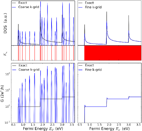
It is worthwhile to discuss some technical aspects of the implementation of KG-formula.Imry (1997); Keleş (2014) Fig. 1 shows two representative cases for a free-electron model 1 nm1 nm cross-section hard-wall NW. On the left column, the coarse-grid case is displayed in which the sparse energy spectrum ends up with the Dirac delta function-derived isolated peaks both for the density of states (DOS) and conductance. The performance of the griding depends on , i.e., the ratio of the energy difference of successive -points, , to the standard deviation of Gaussian broadening, . In the coarse case, the ratio is about 5 at the band edge and further increases through the band dispersion. Since the energy difference between successive conductance steps is larger than the energy broadening, the isolated peaks of both DOS and conductance do not coalesce to reproduce the well-known analytically expected 1D DOS and quantized conduction behavior, a signature of the 1D ballistic transport.van Wees et al. (1988); Ferry, Goodnick, and Bird (2009) Our tests indicate that as the ratio drops below 0.02, the coalescence of isolated peaks starts to yield reasonable DOS and conductance shapes. On the right column of representative fine-grid case, by increasing the number of wave vector, k-points in the energy dispersion curve, the spectrum is made dense enough so that the ratio is set about 0.005 to obtain the analytical behaviors. Hence, this figure signifies the necessity for a dense energy spectrum in achieving ideal quantized conductance steps through the KG-formula.
Notwithstanding, a typical LCBB calculation based on a 3D k-grid (see Fig. 2 (a) and also Appendix A) yields relatively sparse discrete energies. Obviously, the energy spectrum can be made denser (i.e., reduced) by increasing the number of k-points in the 3D grid (i.e., in the expansion basis), however it becomes computationally quite demanding. Instead, regarding the k-space, we construct a dense -grid over the plane perpendicular to the KNW axis or to the axis of one of the crossing wires of a CNW, and obtain the energy dispersion relation of subbands by shifting this plane along that axis of (see Fig. 2 (b) and also Appendix A). Once a reasonable dispersion is obtained, by further interpolating the energy spectrum the KG-formula can be applied to disclose the conductance steps. We call this the dispersion-based approach. It should be noted that in the 3D -grid case which we shall name as the state-based approach, the interpolation is not possible since the 3D eigenvalue problem yields only state energies, without revealing their -dependence. Thus, KG-formula inevitably produces isolated conductance peaks for this state-based case.
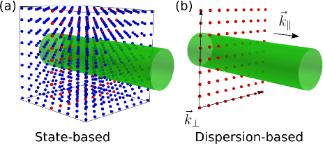
For clean single NWs having no localized states, the dispersion- and state-based approaches yield the same energy spectrum—once constructed with the same number of k-points. However, in the case of CNWs and KNWs the findings of these two approaches deviate: while the state-based approach is able to capture both the states having localized or extended characters, the dispersion-based approach finds only the extended-dispersive states. As we mentioned above, the state-based approach at full performance becomes computationally expensive, so we apply a two-pass approach, where we get the extended states through the dispersion-based approach, followed by a reasonable-budget state-based approach to single out the localized states and to mark the ballistic transport edge (BTE).
III Results
III.1 Crossing Nanowires
We start our transport analysis targeting the low-lying conduction band edge states with the CNWs made up of three crossing 1.5 nm diameter Si NWs oriented along the directions. We choose the Si NWs since it is the major growth orientation within the sub-10-nm diameter size regime.Wu et al. (2004) In Fig. 3, we present the isosurfaces of carrier densities (wave function modulus squares) of the nine lowest electron states, where the first one, CS1 corresponds to the lowest unoccupied molecular orbital (LUMO).not
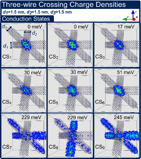
Among them the first six states, CS1-CS6 are observed to be highly localized at the junction of the CNW and diminishes sharply beyond the junction. Energetically, they nest in a window of 51 meV with the individual splittings being governed by the CNW as well as the atomistic point group symmetries as in Si nanocrystals.Bulutay (2007) Separated from this group by about 200 meV, another set of states exists, this time having extended wave functions spread to some portions of the network. As the figure demonstrates, all the states are Si core-derived, with no interface trapping or penetration to the oxide matrix.not
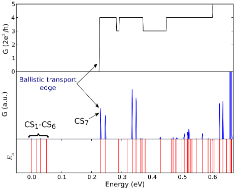
To confirm our isosurface-based interpretations, we compare them with those of the quantum ballistic transport results using the KG-formula. Specifically, we apply the aforementioned two-pass treatment to harness their complementary features to the CNW of Fig. 3. On the top panel of Fig. 4, the dispersion-based approach is displayed where the quantized conductance steps are observed. In the center panel, state-based conduction results are presented. Since the Dirac delta-originated peak values depend on the broadening parameters, only their relative amplitudes and sparsity need to be considered. The energy spectrum underlying the state-based approach is given on the bottom panel. All these results corroborate the isosurface analysis of Fig. 3. Both the dispersion- and state-based approaches pinpoint to the same energy level as the BTE, which is the energy level of CS7 of Fig. 3. It needs to be mentioned that in CNWs we have spotted localized states also above the BTE.Keleş (2014)
Another important remark is that the BTE for CNW is very close to the conduction band minimum (and BTE) of an isolated NW of diameter of 1.5 nm,Keleş et al. (2013) which affirms that indeed the geometric discontinuity of the junction region in CNW is responsible for the additional localized states below BTE. These findings point out that the quantum interference effects play a prominent role at the crossing regions. Any discontinuity over the core material silicon not only excites higher order evanscent modesWeisshaar et al. (1991); Sols et al. (1989) but also results in reflections depending on the state energy and leads to standing waves.
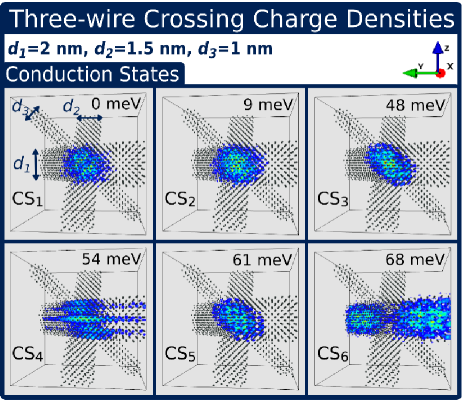
This situation gains a further dimension in the case of CNWs with all-different diameters. In Fig. 5, we present the isosurfaces for charge densities of a three-wire crossing with diameters of 1 nm, 1.5 nm, and 2 nm. We observe that as the difference among the diameters of crossing wires become larger, the electron states at the band edge delocalize, in particular, along the thickest NW. Here, similar to the equal-diameter CNW of Fig. 3, the energy of the first extended state CS4 nearly coincides with the LUMO energy of an isolated 2 nm Si NW.Keleş et al. (2013) In Fig. 6, the isosurfaces are given for the case of wire diameters of 1 nm, 1 nm, and 3 nm. Concerning the LUMO, beyond a diameter contrast, the CNW behaves as isolated NW arrays, as if the other thinner wires are not present. For the higher-lying states, while still extending along the thickest wire, they get more sensitive to the thinner branches. These figures show that the formation and profile of a localized/extended state depends on the relative diameters of the NWs.

III.2 Kinked Nanowires
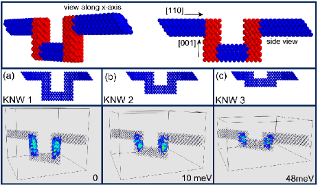
Next, we examine KNWs, here one can benefit from various opportunities for the electronic structure engineering by tuning the diameter and lengths of NW segments or by changing the wire crystallographic orientation. Fig. 7 illustrates the schematic view of a U-shaped KNW where the blue (red) segments are aligned in the [110] ([001]) direction. On the same figure, we specify the variation of LUMO energies as the length of the [001]-aligned segment is decreased. As observed from this figure LUMO is particularly localized to these sections of the KNW forming a standing wave along the [001] wires. Therefore, in agreement with the quantum size effect, the LUMO energy increases as the length of [001] segments decrease.
Focusing on the KNW-3 sample of Fig. 7, on the top panel of Fig. 8, we first subject the KNW to the dispersion-based approach which reproduces the conductance steps, i.e., NW-like dispersive states, starting from the BTE about 0.8 eV above LUMO. On the center panel, we present the conductance values calculated by state-based approach. Note that the onset of the major peaks is very close to the BTE indicated on the top panel.
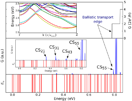
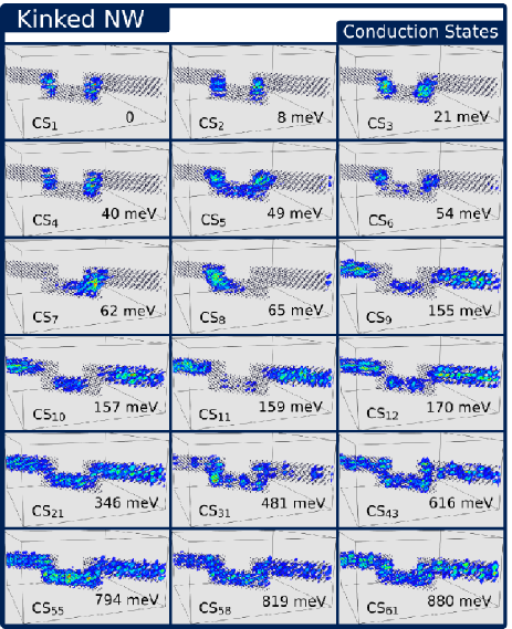
We can classify the states in Fig. 8 according to the relative values of their conductance peaks: (S1) totally localized-bound states, not contributing to the conductance, (S2) quasi-bound states, having low conductance peaks and energetically closer to BTE than to LUMO, and (S3) NW-like extended states which have higher conductance peaks and lie beyond the BTE. As a matter of fact these S3 states are responsible for the full 1D dispersion and contribute to the conductance steps. Dispersion-based approach is not able to capture S1 and S2 states, but identifies the S3 states. The validity of this classification becomes more founded by correlating these observations with the isosurface charge density profiles as presented in Fig. 9 for a selection of conduction states. Here, the first 12 states (CS1-CS12) belong to S1-type states, indicating localized characteristics. The representative states CS21, CS31, and CS43 are S2-type also marked on Fig. 8. As observed in Fig. 9, their isosurfaces also display an extended behavior. Rest of the states given in Fig. 9 are lying at or beyond the BTE, exhibiting NW-like extensions (S3-type).
IV Conclusions
In conclusion, combining wave function analysis with the ballistic transport results we map out the localization behavior of silicon CNWs and KNWs. We find that the BTE can be up to hundreds of millielectron volts above the LUMO, filled in between with a substantial number of localized states. Their 3D wave functions unambigiously display localization around the NW geometric discontinuity regions, such as junctions and bends which excite higher-order evanscent modes and incubate probability amplitude interferences. In contrast to the states close to LUMO, those in the vicinity of BTE possess a proto-conducting character which might contribute to transport through an assisted process, like phonons. Thus, via a realistic atomistic electronic structure analysis, we show that ultraclean Si NW architectures such as CNWs and KNWs should manifest a conduction band tail that exemplifies a disorder-free localization.
Acknowledgements.
This work has been supported by The Scientific and Technological Research Council of Turkey (TÜBİTAK) with Project No. 109R037.Appendix A: LCBB Formalism
In the LCBB method,Wang, Franceschetti, and Zunger (1997); Wang and Zunger (1999); Keleş (2014) the state of the nanostructure can be expressed as the linear combination of bulk Bloch bands
where is the number of bulk primitive unit cells within the large supercell of the nanostructure, is the bulk band index, is the wave vector sampling the BZ of the underlying lattice, and labels the constituent materials, i.e., core or embedding media. The periodic part of the bulk Bloch function can be expanded by the plane waves as
where is the number of reciprocal lattice vectors within an energy cut-off, and is the volume of the primitive cell. These bulk expansion coefficients can be calculated by diagonalizing the bulk Hamiltonian for each point. In our computational implementation, the bulk coefficients are computed by employing the empirical pseudopotential method (EPM).Cohen and Chelikowsky (1988)
The total single-particle Hamiltonian of a nanostructure with the kinetic energy and the ionic potential parts, where the latter describes the atomistic environment within the pseudopotential framework, is expressed by
where is the free electron mass, the direct lattice vector gives the position of the primitive cell and specifies the relative coordinate of a particular atom within the primitive cell. The weight function keeps the information about the composition of the system by taking values 0 or 1 depending on the type of the atom located at the position . is the local screened spherical atomic pseudopotential of atom of the material .
Hamiltonian matrix elements are evaluated within the basis set {} that is {} in the position representation. The resulting Hamiltonian is diagonalized to yield coefficients. The corresponding generalized eigenvalue problem is
where the matrix elements are
Here and are the Fourier transformations of atomic pseudopotentials and weight functions, respectively.
In the case of dispersion-based approach,Keleş (2014) the separation of the -space into and (illustrated in Fig. 2) leads to a separated eigenvalue problem of the form of
which is solved at definite values to obtain the energy dispersion . This form does not put any restriction on the treatment of matrix elements. One should only need to form a planar -grid at a specific point.Keleş (2014)
Appendix B: Oxide Passivation and Atomic Pseudopotentials
An important aspect of the electronic structure calculations is the surface passivation. The surface of an unpassivated nanostructure consists of dangling bonds which introduces surface states lying in the otherwise forbidden band gap. Surface passivation removes these surface states. In our implementation, the surface passivation is provided by embedding the NW structures into a host matrix of SiO2. However, the EPM calculations involving oxygen is rather nontrivial and, moreover, the different lattice structure of SiO2, with reference to Si, causes strain effects.Bulutay (2007) To overcome these obstacles, we introduce an artificial monoatomic wide band gap material that computationally substitutes silica. After constructing the Si NW-based core, all the remaining crystal points within the computational supercell are filled with the artificial oxide atoms. This artificial embedding material has the same dielectric constant of SiO2 and band edge lineup, with respect to Si, however with the diamond structure to prevent complications associated with strain Bulutay (2007).
For the local empirical pseudopotentials of Si and SiO2, we use the functional form introduced by Freidel Friedel, Hybertsen, and Schlüter (1989) These authors suggest an analytical expression to produce the pseudopotential form factor at a given general wave number
| (2) |
We employ their parameters for Si (listed in Table 1).Friedel, Hybertsen, and Schlüter (1989) On the other hand, we have generated pseudopotential parametersKeleş (2014) for the artificial SiO2 (given in in Table 1) which reproduces the experimental band alignments of bulk Si/SiO2 interface as 4.4 eV and 3.4 eV for the valence Keister et al. (1999) and conduction Himpsel et al. (1988) band edges, respectively. The units are arranged such that the pseudopotential form factors come out in Rydbergs and the wave number in Eq. (2) should be in the atomic units (1/Bohr radius). For the plane-wave cut-off energies of EPM, we use 14 Ry for both Si and artificial SiO2.
| Si | 106.0686 | 2.2278 | 0.606 | -1.972 | 5.0 | 0.3 |
|---|---|---|---|---|---|---|
| Matrix-Si | 69.625 | 2.614 | 0.0786 | -19.1433 | 5.99 | 0.335 |
Though the surface chemistry of oxide-passivation requires more elaborate first principles calculations, considering today’s computation limits, we believe that our approach offers a viable alternative for the calculations of oxide-embedded large scale Si nanostructures. Despite the missing surface relaxation and strain effects, the reliability and competence of our computation method has gained confidence in the context of embedded Si and Ge nanocrystals,Bulutay (2007) and in the energetics of single Si NWs and NW networks.Keleş et al. (2013)
The LCBB basis set is constructed by only employing the lowest two bulk conduction bands of the core Si. We tested and observed that the further increase in the number of core bulk bands or the inclusion of the bulk bands of oxide-matrix do not alter the energetics and localization behavior of the states within the energy window very close to band edge (0.5 to 1 eV above the conduction band minimum). Further discussion of LCBB method can be found in the original papersWang, Franceschetti, and Zunger (1997); Wang and Zunger (1999) and in our previous works.Bulutay (2007); Keleş et al. (2013)
References
- Morales and Lieber (1998) A. M. Morales and C. M. Lieber, Science 279, 208 (1998).
- Holmes et al. (2000) J. D. Holmes, K. P. Johnston, R. C. Doty, and B. A. Korgel, Science 287, 1471 (2000).
- Cui et al. (2001) Y. Cui, L. J. Lauhon, M. S. Gudiksen, J. Wang, and C. M. Lieber, Appl. Phys. Lett. 78, 2214 (2001).
- Ma et al. (2003) D. D. D. Ma, C. S. Lee, F. C. K. Au, S. Y. Tong, and S. T. Lee, Science 299, 1874 (2003).
- Wu et al. (2004) Y. Wu, Y. Cui, L. Huynh, C. J. Barrelet, D. C. Bell, and C. M. Lieber, Nano Lett. 4, 433 (2004).
- Martinez, Martinez, and Garcia (2010) R. V. Martinez, J. Martinez, and R. Garcia, Nanotechnology 21, 245301 (2010).
- Özdemir et al. (2011) B. Özdemir, M. Kulakçı, R. Turan, and H. E. Ünalan, Nanotechnology 22, 155606 (2011).
- Barbagiovanni et al. (2014) E. G. Barbagiovanni, D. J. Lockwood, P. J. Simpson, and L. V. Goncharova, Appl. Phys. Rev. 1, 011302 (2014).
- Westwater et al. (1997) J. Westwater, D. P. Gosain, S. Tomiya, S. Usui, and H. Ruda, J. Vac. Sci. Technol., B 15, 554 (1997).
- Tian et al. (2009) B. Tian, P. Xie, T. J. Kempa, D. C. Bell, and C. M. Lieber, Nature Nanotech. 4, 824 (2009).
- Wang et al. (2004) D. Wang, F. Qian, C. Yang, Z. Zhong, and C. M. Lieber, Nano Lett. 4, 871 (2004).
- Jiang et al. (2011) X. Jiang, B. Tian, J. Xiang, F. Qian, G. Zheng, H. Wang, L. Mai, and C. Lieber, Proc. Natl. Acad. Sci. U.S.A. 108, 12212 (2011).
- Mulazimoglu et al. (2013) E. Mulazimoglu, S. Coskun, M. Gunoven, B. Butun, E. Ozbay, R. Turan, and H. E. Unalan, Appl. Phys. Lett. 103, 083114 (2013).
- Tian et al. (2010) B. Tian, T. Cohen-Karni, Q. Qing, X. Duan, P. Xie, and C. M. Lieber, Science 329, 830 (2010).
- Cook and Varga (2011) B. G. Cook and K. Varga, Appl. Phys. Lett. 98, 052104 (2011).
- Xu et al. (2013) L. Xu, Z. Jiang, Q. Qing, L. Mai, Q. Zhang, and C. M. Lieber, Nano Lett. 13, 746 (2013).
- Jiang et al. (2012) Z. Jiang, Q. Qing, P. Xie, R. Gao, and C. M. Lieber, Nano Lett. 12, 1711 (2012).
- Qing et al. (2014) Q. Qing, Z. Jiang, L. Xu, R. Gao, L. Mai, and C. M. Lieber, Nature Nanotech. 9, 142 (2014).
- Xu et al. (2014) L. Xu, Z. Jiang, L. Mai, and Q. Qing, Nano Lett. 14, 3602 (2014).
- Sheng (1997) W.-D. Sheng, J. Appl. Phys. 81, 6210 (1997).
- Ferry, Goodnick, and Bird (2009) D. K. Ferry, S. M. Goodnick, and J. Bird, Transport in Nanostructures, 2nd ed. (Cambridge University Press, New York, USA, 2009).
- Datta et al. (1986) S. Datta, M. R. Melloch, S. Bandyopadhyay, and M. S. Lundstrom, Appl. Phys. Lett. 48, 487 (1986).
- Timp et al. (1988) G. Timp, H. Baranger, P. deVegvar, J. Cunningham, R. Howard, R. Behringer, and P. Mankiewich, Phys. Rev. Lett. 60, 2081 (1988).
- Aihara, Yamamoto, and Mizutani (1993) K. Aihara, M. Yamamoto, and T. Mizutani, Appl. Phys. Lett. 63, 3595 (1993).
- Tilke et al. (2003) A. Tilke, F. Simmel, H. Lorenz, R. Blick, and J. Kotthaus, Phys. Rev. B 68, 075311 (2003).
- Weisshaar et al. (1991) A. Weisshaar, J. Lary, S. M. Goodnick, and V. K. Tripathi, J. Appl. Phys. 70, 355 (1991).
- Shao, Porod, and Lent (1994) Z. A. Shao, W. Porod, and C. S. Lent, Phys. Rev. B 49, 7453 (1994).
- Sengupta, Chakrabarti, and Chattopadhyay (2005) S. Sengupta, A. Chakrabarti, and S. Chattopadhyay, Phys. Rev. B 71, 134204 (2005).
- Martin (2004) R. M. Martin, Electronic Structure, 1st ed. (Cambridge University Press, Cambridge, UK, 2004).
- Neophytou et al. (2008) N. Neophytou, A. Paul, M. Lundstrom, and G. Klimeck, IEEE Trans. Electron Devices 55, 1286 (2008).
- Persson et al. (2008) M. P. Persson, A. Lherbier, Y.-M. Niquet, F. Triozon, and S. Roche, Nano Lett. 8, 4146 (2008).
- Kim and Fischetti (2011) J. Kim and M. V. Fischetti, J. Appl. Phys. 110, 033716 (2011).
- Wang, Franceschetti, and Zunger (1997) L.-W. Wang, A. Franceschetti, and A. Zunger, Phys. Rev. Lett. 78, 2819 (1997).
- Wang and Zunger (1999) L.-W. Wang and A. Zunger, Phys. Rev. B 59, 15806 (1999).
- Keleş et al. (2013) Ü. Keleş, B. Liedke, K.-H. Heinig, and C. Bulutay, Appl. Phys. Lett. 103, 203103 (2013).
- Urbach (1953) F. Urbach, Phys. Rev. 92, 1324 (1953).
- Pan et al. (2008) Y. Pan, F. Inam, M. Zhang, and D. A. Drabold, Phys. Rev. Lett. 100, 206403 (2008).
- Leu, Svizhenko, and Cho (2008) P. Leu, A. Svizhenko, and K. Cho, Phys. Rev. B 77, 235305 (2008).
- Shiri et al. (2008) D. Shiri, Y. Kong, A. Buin, and M. P. Anantram, Appl. Phys. Lett. 93, 073114 (2008).
- Niquet, Delerue, and Krzeminski (2012) Y.-M. Niquet, C. Delerue, and C. Krzeminski, Nano Lett. 12, 3545 (2012).
- Wu, Neaton, and Grossman (2009) Z. Wu, J. B. Neaton, and J. C. Grossman, Nano Lett. 9, 2418 (2009).
- Svizhenko, Leu, and Cho (2007) A. Svizhenko, P. Leu, and K. Cho, Phys. Rev. B 75, 125417 (2007).
- Lherbier et al. (2008) A. Lherbier, M. Persson, Y.-M. Niquet, F. Triozon, and S. Roche, Phys. Rev. B 77, 085301 (2008).
- Kubo (1957) R. Kubo, J. Phys. Soc. Jpn. 12, 570 (1957).
- Greenwood (1958) D. A. Greenwood, Proc. Phys. Soc. 71, 585 (1958).
- Akkermans and Montambaux (2007) E. Akkermans and G. Montambaux, Mesoscopic Physics of Electrons and Photons, 1st ed. (Cambridge University Press, New York, 2007).
- Imry (1997) Y. Imry, Introduction to Mesoscopic Physics, 1st ed. (Oxford University Press, New York, 1997).
- Keleş (2014) Ü. Keleş, Silicon nanowire-based complex structures: a large-scale atomistic electronic structure and ballistic transport, Ph.D. thesis, Bilkent University, Ankara, Turkey (unpublished, 2014).
- van Wees et al. (1988) B. J. van Wees, H. van Houten, C. W. J. Beenakker, J. G. Williamson, L. P. Kouwenhoven, D. van der Marel, and C. T. Foxon, Phys. Rev. Lett. 60, 848 (1988).
- (50) We should note that there would be other interface states as well. However, as we only include the bulk silicon Bloch functions in the LCBB basis set, we do not probe most of such states.
- Bulutay (2007) C. Bulutay, Phys. Rev. B 76, 205321 (2007).
- Sols et al. (1989) F. Sols, M. Macucci, U. Ravaioli, and K. Hess, Appl. Phys. Lett. 54, 350 (1989).
- Cohen and Chelikowsky (1988) M. L. Cohen and J. R. Chelikowsky, Electronic Structure and Optical Properties of Semiconductors, 8th ed. (Springer-Verlag, Berlin, 1988).
- Friedel, Hybertsen, and Schlüter (1989) P. Friedel, M. S. Hybertsen, and M. Schlüter, Phys. Rev. B 39, 7974 (1989).
- Keister et al. (1999) J. W. Keister, J. E. Rowe, J. J. Kolodziej, H. Niimi, T. E. Madey, and G. Lucovsky, J. Vac. Sci. Technol. B 17, 1831 (1999).
- Himpsel et al. (1988) F. J. Himpsel, F. R. McFeely, A. Taleb-Ibrahimi, J. A. Yarmoff, and G. Hollinger, Phys. Rev. B 38, 6084 (1988).