Strain induced mobility modulation in single-layer MoS2
Abstract
In this paper the effect of biaxial and uniaxial strain on the mobility of single-layer MoS2 for temperatures T 100 K is investigated. Scattering from intrinsic phonon modes, remote phonon and charged impurities are considered along with static screening. Ab-initio simulations are utilized to investigate the strain induced effects on the electronic bandstructure and the linearized Boltzmann transport equation is used to evaluate the low-field mobility under various strain conditions. The results indicate that the mobility increases with tensile biaxial and tensile uniaxial strain along the armchair direction. Under compressive strain, however, the mobility exhibits a non-monotonic behavior when the strain magnitude is varied. In particular, with a relatively small compressive strain of 1% the mobility is reduced by about a factor of two compared to the unstrained condition, but with a larger compressive strain the mobility partly recovers such a degradation.
pacs:
72.20.Fr, 73.63.-b, 71.15.MbI Introduction
Single and few-layers of transition metal dichalcogenides show promising electronic, optical, and mechanical properties and are considered as potential candidates for future electronic applications Neto and Novoselov (2011). Because of weak inter-layer van der Waals bonds in their layered structure, single to few-layers of these materials can be obtained by mechanical or chemical exfoliation techniques Novoselov et al. (2005); Ayari et al. (2007); Ramakrishna Matte et al. (2010). Among these materials single-layer MoS2 has attracted the attention of scientistsKorn et al. (2011); Splendiani et al. (2010); Mak et al. (2010, 2013). Single-layer MoS2 has a direct band gap of 1.8 to 1.9 eV Mak et al. (2010); Splendiani et al. (2010), which makes it suitable for various electronic applications Yoon et al. (2011). It has been shown that the application of compressive and tensile biaxial strain results in an indirect bandgap Tabatabaei et al. (2013); Feng et al. (2012); Ghorbani-Asl et al. (2013). An MOS transistor based on this material has demonstrated a ratio of , a relatively steep sub-threshold swing of 74 mV/dec and an extremely small off-current of 25 fA/m Radisavljevic et al. (2011), moreover possible applications to hetero-junction inter-layer tunneling FETs have also been proposed and theoretically investigated Li et al. (2014). Room temperature mobility of n-type single-layer MoS2 has been reported to be in the range of 0.5–3 cm2/(Vs) and can be increased to about 200 cm2/(Vs) with the use of high- dielectrics Radisavljevic et al. (2011).
The low-field mobility is one of the most important transport properties for a large number of physical systems and electronic devices. A comprehensive study of strain effects on the mobility of single layer MoS2, however, is missing. In the present work, the effects of biaxial and uniaxial strain on the low-field mobility of single-layer MoS2 is investigated by using ab-initio simulations along with the linearized Boltzmann transport equation (BTE) Paussa and Esseni (2013). Scattering rates due to intrinsic phonon, charge impurities, and remote phonon are taken into account.
II Bandstructure and Scattering Rates
In the first part of this section, some details about the ab-initio calculations of the electronic bandstructure in the presence of strain are discussed. Thereafter, the formulation of various scattering rates is described.
II.1 Bandstructure
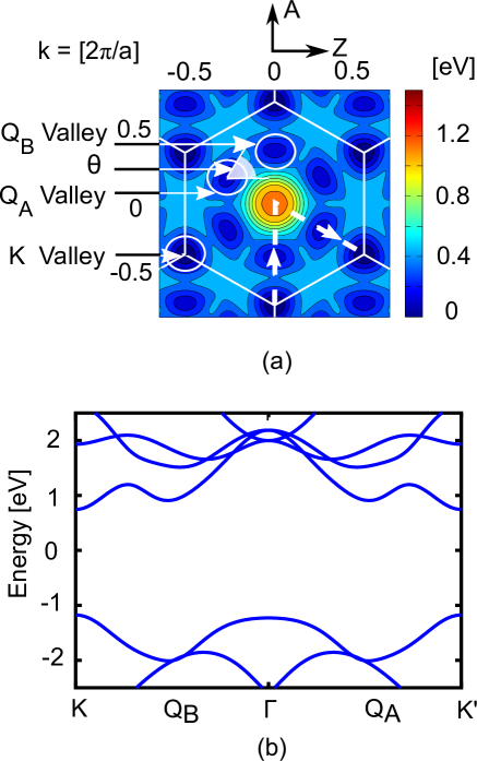
We carry out first-principle simulations based on the density-functional theory (DFT) along with the local density approximation (LDA) as implemented in the SIESTA code Soler et al. (2002); Han et al. (2011); Lebegue and Eriksson (2009) to investigate the relevant electronic properties of a single layer MoS2 under strain. While DFT-LDA, in general, underestimates band gaps, the resulting dispersion of individual bands, i.e., effective masses and energy differences between valleys, is less problematic Kaasbjerg et al. (2012). A cutoff energy equal to Ry is used and a vacuum separation of Å is adopted, which is sufficient to hinder interactions between adjacent layers. Sampling of the reciprocal space Brillouin zone (BZ) is performed by a Monkhorst-Pack grid of -points. Calculations begin with the determination of the optimized geometry, that is the configuration in which the residual Hellmann-Feynman forces acting on atoms are smaller than eV/Å. The calculated lattice constant of unstrained single-layer MoS2 is 3.11 Å that has a good agreement with the reported value in Ref. Chang et al., 2013; Ataca and Ciraci, 2011. Fig. 1(a) shows the energy contours of the conduction-band in the first BZ for unstrained single layer MoS2. In an unstrained material the lowest and the second lowest minimum in the conduction band are denoted as K-valley and Q-valley, respectively. The 6 K valleys are degenerate in the unstrained and in all the strained conditions explored in this paper. The 6 Q-valleys are degenerate in unstrained conditions, while under uniaxial strain they split into 4 QA-valleys and 2 QB-valleys with different effective masses and energy minima, as discussed and illustrated in Sec. IV. The energy distance between K-valley and Q-valley for unstrained material is evaluated to be 160 meV, in agreement with Ref. Kaasbjerg et al., 2012. Fig. 1(b) shows the calculated DFT-LDA band structure and depicts a direct band gap of 1.92 eV at the K-point which is very close to the experimentally measured value of 1.85 eV Splendiani et al. (2010).
II.2 Scattering with MoS2 phonon modes
Scattering rates due to intrinsic phonons (including acoustic, optical and polar-optical phonons), to remote phonons and to charged impurities are taken into account. Piezoelectric coupling to the acoustic phonons is only important at low temperatures and is neglected in this work Kaasbjerg et al. (2013). If the surrounding dielectric provides a large energy barrier for confining electrons in the MoS2 layer, the envelope function of mobile electrons can be approximated as with Ma and Jena (2014), where is the area normalization factor, is the in-plane two-dimensional wave vector, is the thickness of single layer MoS2 and is the in-plane position vector. The scattering rates for the acoustic and optical phonon are discussed first.
Using Fermi’s golden rule the scattering rate from an initial state in valley to the final state in valley can be written as
| (1) |
where is the matrix element for the mentioned transition and is the phonon energy that may depend on . The intra-valley transitions () assisted by acoustic phonons can be approximated as elastic and the rate is given by
| (2) |
where is the Boltzmann constant, is the absolute temperature, is the acoustic the deformation potential, [gr/cm2] is the mass density and is the sound velocity of single layer MoS2. On the other hand, the rate of inelastic phonon scattering, including intra and inter-valley optical phonons, and inter-valley acoustic phonons, can be expressed as
| (3) |
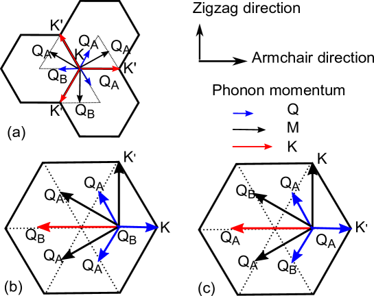
where is the acoustic/optical deformation potential for a transition between valleys and , is the phonon energy, and is the phonon occupation (upper and lower sign denote phonon absorption and phonon emission, respectively). The phonon assisted inter-valley transitions considered in this work, and the corresponding phonon momentum are shown in Fig. 2. In our calculations, we employed the deformation potentials and phonon energies from Ref. Li et al., 2013 that are reported in Table 1 and Table 2. It should be noted that the same deformation potentials are used for QA and QB valleys.
II.3 Remote Phonon Scattering
Another important scattering source considered in this work is the remote phonon or surface-optical (SO) phonon scattering mechanism. The source of this scattering is in the surrounding dielectrics via long-range Coulomb interactions, provided that the dielectrics support polar vibrational modes. By assuming semi-infinite oxides and neglecting the possible coupling to the plasmons of the two-dimensional material, the energy dispersion of SO phonons can be obtained by solving the secular equation Ong and Fischetti (2013)
| (4) |
where the thickness of the single layer MoS2 is set to Å Yue et al. (2012), is the dielectric constant of the two-dimensional material (single layer MoS2 in this work), the index box and tox denote the back-oxide () and the top-oxide (), respectively, and for MoS2 is set to 7.6 Ma and Jena (2014). A numerical solution of Eq. 4 shows that the frequency of remote phonon has a very weak dependence on , that consequently we neglected in our calculations by setting in Eq. 4. With this approximation, Eq. 4 simplifies to , that we solved by using the single polar phonon expression for the in each oxide:
| (5) |
where and are the high and low frequency dielectric constant, respectively, and is the frequency of the polar phonon in the oxide. We could provide analytical solution for Eq. 5 and express as: and for as , where , and . Table 3 reports the parameters of dielectric materials that are studied in this work and indicates the corresponding calculated SO phonon frequencies. The scattering matrix element of remote phonon can be written as Ong and Fischetti (2013):
| (6) |
| (7) |
Scattering with SO phonon mode is inelastic and we consider only intra-valley transitions. The corresponding transition rate is
| (8) |
where and are the SO phonon occupation number and energy, respectively.
II.4 Scattering with Coulomb Centers
To investigate the effect of the dielectric environment on the scattering of carriers from charged impurities located inside the single layer MoS2, we assume that the charged impurities are located in the center of the single layer MoS2 thickness, that is at . The Fourier transform of the scattering potential due to a charged impurity located at can be written as Esseni et al. (2011)
| (9) |
where is the elementary charge, and and can be written as
| (10) |
and
| (11) |
Using Eq. 9, the form and assuming intra-valley transitions for scattering with charged impurities, the transition matrix elements take the form
| (12) |
where . Eq. 12 expresses the matrix element for a Coulomb center located in and does not account for the screening produced by the free carriers in MoS2; such a screening effect is introduced according to the dielectric matrix approach discussed in Sec. II.5. The overall matrix element produced by a set of Coulomb centers randomly distributed at positions is known to be affected by the statistical properties of the distribution and, in particular, by a possible correlation between the position of Coulomb centers. In this paper we do not address these difficulties and simply write the overall matrix element as , where is the impurity density per unit area and is given by Eq. 12. Scattering charged impurities is treated as elastic and the rate is therefore given by
| (13) |
II.5 Screening
The effect of static screening produced by the electrons in the MoS2 conduction band is described by using the dielectric function approach Esseni et al. (2011), so that the screened matrix element in valley is obtained by solving the linear problem:
| (14) |
where are the unscreened matrix element. As can be seen in Fig. 1(a), there are three different valleys in strained single layer MoS2 (K, QA and QB valleys), hence , {K, QA, QB}. In Eq. 14, is the dielectric matrix which is introduced as:
| (15) |
where is the Kronecker symbol (1 if , otherwise zero), and are the polarization factor and unit-less screening form factor, respectively Esseni et al. (2011). In the case at study the dielectric matrix can be analytically inverted to evaluate screened matrix elements as:
| (16) |
The static dielectric function approach described above has been directly used for the scattering due to charged impurities, while the situation is admittedly more complicated for phonon scattering. For the inelastic, intervalley phonon transitions described in Table 1 and Table 2 the relatively large phonon wave-vector (see also Fig. 2) and the non-null phonon energies suggest that it is safe to leave these transitions unscreened, because the dynamic descreening and the large phonon wave-vectors make the screening very ineffective. Arguments concerning screening for intra-valley acoustic phonons are more subtle and controversial and a thorough discussion for inversion layer systems can be found in Ref. Fischetti and Laux, 1993. We here decided to leave also intra-valley acoustic phonons unscreened, which is the choice employed in essentially all the studies concerning transport in inversion layers that the authors are aware of. The screening of the SO phonon scattering is also a delicate subject, because the polar phonon modes of the high- dielectrics can couple with the collective excitations of the electrons in the MoS2 layer and thus produce coupled phonon-plasmon modes Ong and Fischetti (2013); Fischetti and Laux (1993), whose treatment is further complicated by the possible occurrence of Landau damping Ong and Fischetti (2013); Fischetti and Laux (1993); Toniutti et al. (2012). In this paper we do not attempt a full treatment of the coupled phonon-plasmon modes Ong and Fischetti (2013); Fischetti and Laux (1993), but instead show in in Sec. IV results for the two extreme cases of either unscreened SO phonons or SO phonons screened according to the static dielectric function. We can anticipate that while the inclusion of static screening in SO phonons implies a significant mobility enhancement compared to the unscreened case, the mobility dependence on the strain and on the dielectric constant of the high- dielectrics is not significantly affected by the treatment of screening for SO phonons.
III Mobility Calculation
Acoustic, optical, polar-optical, remote phonon, and charged impurity scatterings are considered for the calculation of low-field mobility. As it will be discussed in the next section, the bandstructure for QA and QB valleys is not isotropic and the mobility shows direction-dependence, hence we calculated mobility by solving numerically the linearized Boltzmann Transport Equation (BTE) according to the approach described in Ref. Paussa and Esseni, 2013, which does not introduce any simplifying assumption in the BTE solution. In particular, mobility has been calculated along the armchair and zigzag directions and strain has been also studied for the uniaxial configuration along either armchair or zigzag direction, as well as for the biaxial configuration.
In order to describe in more detail the mobility calculation procedure, we first recall that the longitudinal direction of QA-valley is neither the armchair nor the zigzag direction, and Fig. 1(a) shows that is the angle describing the valley orientation with respect to the zigzag direction in k-space (i.l. armchair direction in real space). Let us now consider first the case of the mobility of valley along the armchair direction, that can be written by definition as , where is the current component in the armchair direction for the valley induced by the electric field along armchair direction. The current can be expressed as in terms of the current components , along, respectively, the longitudinal and transverse direction of the valley . By denoting the longitudinal () and transverse component () of the electric field as and , the currents and in turn can be written as and , where , and are the entries of the two by two mobility matrix in the valley coordinate system Esseni et al. (2011). Consequently we finally obtain:
| (17) |
By following a similar procedure, the mobility of the valley along the zigzag direction can be written as:
| (18) |
For the circular and elliptical bands employed in our calculations (see Fig. 3(g)), is zero for symmetry reasons Esseni et al. (2011). After calculating the mobility for each valley, the overall mobilities and are obtained as the average of the mobility in the different valleys weighted by the the corresponding electron density.
Eq. 17 and Eq. 18 allow us to calculate the mobility and from the longitudinal and the transverse mobility of the valley which are the mobilities obtained from the linearized BTE when the electric field is either in the longitudinal or in the transverse direction of the valley . As already said, the and have been obtained by using the approach of Ref. Paussa and Esseni, 2013, whose derivation for the case at study in this work can be summarized as follows. The out of equilibrium occupation function for the valley in the presence of a field is written as
| (19) |
where is the equilibrium Fermi-Dirac distribution function, is either the longitudinal or the transverse direction of the valley and is the wavevector in the valley coordinate system. Eq. 19 is a definition of , which is the unknown function of the linearized BTE problem. For a two-dimensional system the linearized BTE can be written as Paussa and Esseni (2013)
| (20) |
where is the component of the group velocity of valley and, for convenience of notation, we have introduced the quantity
| (21) |
To numerically solve Eq. 20, we employed the discretization scheme introduced in Ref. Paussa and Esseni, 2013: is discretized according to a uniform angular step and also a uniform energy step. The discrete values of the wave-vector magnitude correspond to one of the discrete energy values and the generic discrete wave-vector is identified by the magnitude and the angle (with being a positive integer number). For each scattering mechanism, by converting the integral over in an integral over the energy and the angle and then using the above mentioned discretization, Eq. 20 can be rewritten as:
| (22) |
Eq. 22 is a linear problem for the discretized unknown values written in terms of the coefficients and defined as
| (23) |
| (24) |
where the non-zero entries of the matrix representing the linear problem are governed by the Kronecker symbols , that are defined so to enforce energy conservation Paussa and Esseni (2013).
Eq. 22 has been written for a single scattering mechanism. In order to accommodate several scattering mechanisms in our calculations, we do not resort to an approximated treatment based on the Matthiessen rule Esseni and Driussi (2011), but instead follow Ref. Paussa and Esseni, 2013 and notice that Eq. 22 can be written in the concise matrix notation , where is a matrix specific of the scattering mechanisms , is the unknown vector and is the vector at the right hand side of Eq. 22 and consisting of known quantities. Hence the unknown vector corresponding to several scattering mechanisms can be obtained by solving the linear problem
| (25) |
where Eq. 22–Eq. 24 will totally define the entries of the matrix for each scattering mechanism.
IV Results and Discussions
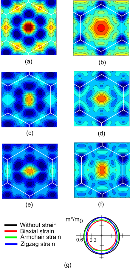
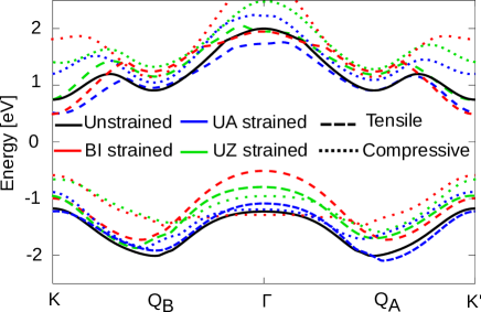
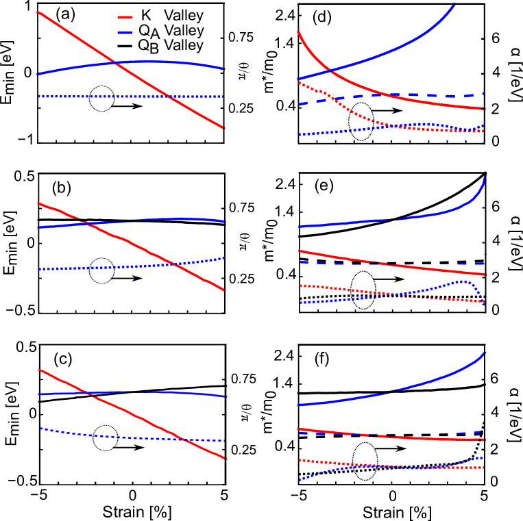
Fig. 3 shows the energy contours of the conduction-band in the first BZ for strained single layer MoS2. In an unstrained material the lowest and the second lowest minimum in the conduction band are denoted as K-valley and Q-valley, respectively. The 6 Q-valleys are degenerate for unstrained and biaxial strain conditions. With the application of uniaxial strain, however, they split into 4 QA-valleys and 2 QB-valleys with different effective masses and energy minima. Fig. 4 illustrates the bandstructure of unstrained and strained single layer MoS2 including K, QA, and QB valleys. Under compressive strain one of the QA or QB valleys becomes the lowest valley.
The energy distance between these K-valley and Q-valley for unstrained material is evaluated to be 160 meV, in agreement with Ref. Kaasbjerg et al., 2012. Tensile strain increases this energy distance, which is instead reduced by a compressive strain. In particularly, a relatively large compressive strain lowers the energy of Q-valley so that it becomes the lowest valley as shown in Fig. 5(a)-(c). Here we can anticipate that, while under tensile strain one can neglect the scattering between Q and K-valleys, under compressive strain this type of scattering can significantly affect the mobility. Assuming a non-parabolic dispersion relation , the longitudinal and transverse effective mass and also the non-parabolicity factor are extracted from the DFT-calculated electronic bandstructure and reported in Fig. 5(d)-(f). As can be seen in Fig. 5(a)-(c), under compressive uniaxial strain the energy minima of all K- and Q-valleys are quite close, while at large compressive biaxial strain the K-valley lie at higher energy and their contribution to mobility can be neglected.
We compare in Table 4 our calculated mobilities at various carrier concentrations with the experimental data reported in Ref. Radisavljevic and Kis, 2013 for unstrained single-layer MoS2 embedded between SiO2 and HfO2 with impirity density 4 . At K the effect of piezoelectric can be ignored Kaasbjerg et al. (2013). Very good agreement with experimental data validates the bandstructure and mobility models employed in this work.
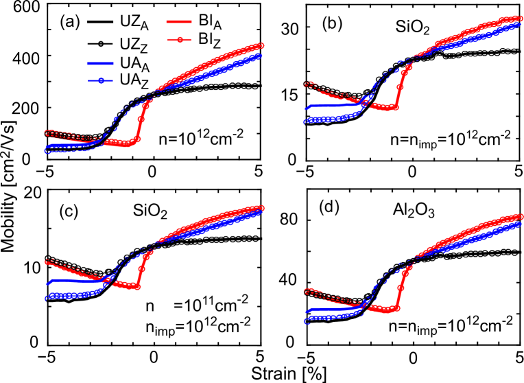
The strain-dependency of intrinsic phonon limited mobility is presented in Fig. 6(a). Apparently, the effects of compressive and tensile strain on mobility are very different, which can be mainly explained by considering the role of inter-valley scattering. For example, with tensile strain the minimum energies of QA and QB-valleys are much higher than that of K-valley, which suppresses inter-valley scattering. Under compressive strain, instead, the inter-valley scattering cannot be neglected because of the smaller energy difference between these valleys. With tensile biaxial strain, the mobility increases because of the reduction of the effective mass and also the increase of the energy difference between K and Q-valleys, which results in the reduction of the inter-valley scattering rate. With a tensile biaxial strain of the phonon limited mobility becomes higher than that of unstrained material. In contrast, a compressive biaxial strain of 0.8 strongly reduces the mobility due to the reduction of energy difference between K and Q-valleys (see Fig. 5(a)) and increased inter-valley scattering. With further increase of compressive biaxial strain, Q-valleys become the lowest ones and thus dominate the mobility. At a strain value of about the contribution of K-valleys to mobility becomes negligible and the mobility behavior is completely determined by the Q-valleys. Longitudinal and transverse effective masses of Q-valleys are not equal and are somewhat changed by strain, however, the different angular dependency of mobility along the armchair and zigzag direction tends to compensate the changes of effective masses and the overall mobility remains nearly constant at larger compressive strain values.
Under tensile uniaxial strain the mobility is hardly affected by a strain along the zigzag direction, while it increases for strain along the armchair direction. In both cases the variation of the effective mass and non-parabolicity factor with strain determine the mobility behavior. Under a compressive uniaxial strain along the armchair direction, QA becomes the lowest valley, while for a strain along the zigzag direction QB is the lowest one. These results emphasize that the contribution of both QA and QB valley should be included for an accurate calculation of mobility. Under a compressive strain of about 1.5% the mobilities are strongly reduced, but they remain nearly constant for larger strain magnitudes. Moreover, we notice that for a strain along the zigzag direction, the mobility along the strain direction becomes slightly larger than the mobility in the armchair direction.
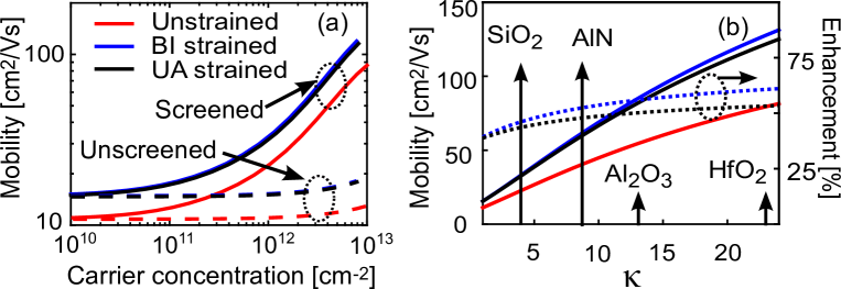
Fig. 6(b) reports the mobility in the presence of intrinsic phonon and charged impurity scattering. The top and bottom oxide are assumed to be SiO2 and both carrier and impurity concentrations are cm-2. Except for a global reduction of the mobility, the behavior of the mobility with strain is similar to Fig. 6(a) corresponding to phonon limited mobility. The results presented in Fig. 6(c) correspond to the same parameters as in Fig. 6(b), except for a reduction of carrier concentration to cm-2. As the carrier concentration decreases the effect of static screening becomes weaker and the mobility is further reduced. Fig. 6(d) illustrates the mobility as a function of strain with the same parameters used in Fig. 6(b), expect for the top and bottom gate oxide which is Al2O3. A high- dielectric implies a larger dielectric screening and increases the mobility. Under this condition, with a tensile biaxial strain of 5% and a tensile uniaxial strain of 5% along the armchair direction the mobility increases by 53% and 43%, respectively, compared to an unstrained single-layer MoS2. For a better comparison, Fig. 7 shows the room temperature mobility versus carrier concentration and also versus the dielectric constant for the unstrained material and for 5% tensile strain in either a biaxial or a uniaxial configuration along the armchair direction with an impurity density equal to cm-2. As can be seen in Fig. 7(a), because of screening the mobility increases with the carrier concentration for both unstrained and strained cases. Fig. 7(b) indicates that the strain induced mobility enhancement with high- dielectric materials is slightly larger than that with low- materials.
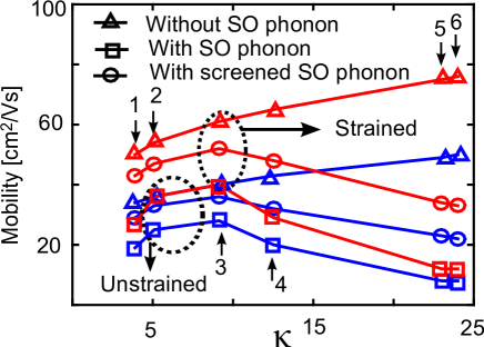
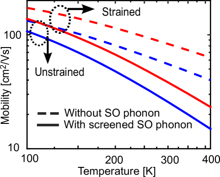
The effect of unscreened and screened remote phonon scattering on the mobility of unstrained and 5% biaxial strained single layer MoS2 are compared in Fig. 8. Except for a global increase of mobility values. The mobility dependence on the dielectric constant is not significantly affected by the screening of SO phonons. As can be seen, for relatively small values, mobility improves with increasing because of the dielectric screening of charged impurities Ma and Jena (2014). At high values, however, the mobility decrease with increasing because the corresponding smaller SO phonon energies (see Table 3) tend to increase momentum relaxation time via SO phonons. For the conditions considered in Fig. 8(temperature, carrier and impurity concentrations, and semi-infinite dielectrics with SiO2 as the bottom oxide), AlN appears to be the optimal top dielectric material for strained and also unstrained single layer MoS2. Fig. 9 shows the temperature dependency of the mobility for unstrained and 5% biaxial strain with HfO2 as the top oxide. As expected the effect of inelastic remote phonons increases with temperature for both unstrained and strained cases. Therefore, it is expected that the optimal material as a top dielectric for temperatures above(bellow) 300 K, should have a lower(higher)- compared to AlN.
V Conclusion
A comprehensive theoretical study on the role of strain on the mobility of single-layer MoS2 is presented. DFT calculations are used to obtain the effective masses and energy minima of the contributing valleys. Thereafter, the linearized BTE is solved for evaluating the mobility, including the effect of intrinsic phonons, remote phonons, and screened charged impurities. The results indicate that, a tensile strain increases the mobility, while compressive strain reduces the mobility. Furthermore, biaxial strain and uniaxial strain along the armchair direction increase the mobility more effectively. The strain-dependency of the mobility of MoS2 is rather complicated and strongly depends on the relative positions of Q and K-valleys and the corresponding inter-valley scattering. The presented results pave the way for a possible strain engineering of the electronic transport in MoS2 based electron devices.
References
- Ataca and Ciraci (2011) Ataca, C., and S. Ciraci (2011), J. Phys. Chem. C 115 (27), 13303.
- Ayari et al. (2007) Ayari, A., E. Cobas, O. Ogundadegbe, and M. S. Fuhrer (2007), J. Appl. Phys. 101 (1), 014507.
- Chang et al. (2013) Chang, C.-H., X. Fan, S.-H. Lin, and J.-L. Kuo (2013), Phys. Rev. B 88 (19), 195420.
- Esseni and Driussi (2011) Esseni, D., and F. Driussi (2011), IEEE Tran. Electron Devices 58 (8), 2415.
- Esseni et al. (2011) Esseni, D., P. Palestri, and L. Selmi (2011), Nanoscale MOS Transistors (Cambridge University Press, Cambridge).
- Feng et al. (2012) Feng, J., X. Qian, C.-W. Huang, and J. Li (2012), Nature Photon. 6 (12), 866.
- Fischetti and Laux (1993) Fischetti, M. V., and S. E. Laux (1993), Phys. Rev. B 48 (4), 2244.
- Ghorbani-Asl et al. (2013) Ghorbani-Asl, M., S. Borini, A. Kuc, and T. Heine (2013), Phys. Rev. B 87 (23), 235434.
- Han et al. (2011) Han, S., H. Kwon, S. K. Kim, S. Ryu, W. S. Yun, D. Kim, J. Hwang, J.-S. Kang, J. Baik, H. Shin, et al. (2011), Phys. Rev. B 84 (4), 045409.
- Kaasbjerg et al. (2012) Kaasbjerg, K., K. S. Thygesen, and K. W. Jacobsen (2012), Phys. Rev. B 85 (11), 115317.
- Kaasbjerg et al. (2013) Kaasbjerg, K., K. S. Thygesen, and A.-P. Jauho (2013), Phys. Rev. B 87, 235312.
- Konar et al. (2010) Konar, A., T. Fang, and D. Jena (2010), Phys. Rev. B 82 (11), 115452.
- Korn et al. (2011) Korn, T., S. Heydrich, M. Hirmer, J. Schmutzler, and C. Schüller (2011), Appl. Phys. Lett. 99 (10), 102109.
- Lebegue and Eriksson (2009) Lebegue, S., and O. Eriksson (2009), Phys. Rev. B 79 (11), 115409.
- Li et al. (2014) Li, M. O., D. Esseni, G. Snider, D. Jena, and H. G. Xing (2014), J. Appl. Phys. 115 (7), 074508.
- Li et al. (2013) Li, X., J. T. Mullen, Z. Jin, K. M. Borysenko, M. B. Nardelli, and K. W. Kim (2013), Phys. Rev. B 87 (11), 115418.
- Ma and Jena (2014) Ma, N., and D. Jena (2014), Phys. Rev. X 4 (1), 011043.
- Mak et al. (2013) Mak, K. F., K. He, C. Lee, G. H. Lee, J. Hone, T. F. Heinz, and J. Shan (2013), Nature Mater. 12 (3), 207.
- Mak et al. (2010) Mak, K. F., C. Lee, J. Hone, J. Shan, and T. F. Heinz (2010), Phys. Rev. Lett. 105 (13), 136805.
- Neto and Novoselov (2011) Neto, A., and K. Novoselov (2011), Rep. Prog. Phys. 74 (8), 82501.
- Novoselov et al. (2005) Novoselov, K., D. Jiang, F. Schedin, T. Booth, V. Khotkevich, S. Morozov, and A. Geim (2005), Proc. Nat. Acad. Sci. 102 (30), 10451.
- Ong and Fischetti (2013) Ong, Z.-Y., and M. V. Fischetti (2013), Phys. Rev. B 88, 045405.
- Paussa and Esseni (2013) Paussa, A., and D. Esseni (2013), J. Appl. Phys. 113 (9), 093702.
- Perebeinos and Avouris (2010) Perebeinos, V., and P. Avouris (2010), Phys. Rev. B 81 (19), 195442.
- Radisavljevic and Kis (2013) Radisavljevic, B., and A. Kis (2013), Nature Mater. 12 (9), 815.
- Radisavljevic et al. (2011) Radisavljevic, B., A. Radenovic, J. Brivio, V. Giacometti, and A. Kis (2011), Nature Nanotech. 6 (3), 147.
- Ramakrishna Matte et al. (2010) Ramakrishna Matte, H., A. Gomathi, A. K. Manna, D. J. Late, R. Datta, S. K. Pati, and C. Rao (2010), Angew. Chem. Int. Ed. 122 (24), 4153.
- Soler et al. (2002) Soler, J. M., E. Artacho, J. D. Gale, A. García, J. Junquera, P. Ordejón, and D. Sánchez-Portal (2002), J. Phys.: Condens. Matter 14 (11), 2745.
- Splendiani et al. (2010) Splendiani, A., L. Sun, Y. Zhang, T. Li, J. Kim, C.-Y. Chim, G. Galli, and F. Wang (2010), Nano Lett. 10 (4), 1271.
- Tabatabaei et al. (2013) Tabatabaei, S. M., M. Noei, K. Khaliji, M. Pourfath, and M. Fathipour (2013), J. Appl. Phys. 113 (16), 163708.
- Toniutti et al. (2012) Toniutti, P., P. Palestri, D. Esseni, F. Driussi, M. De Michielis, and L. Selmi (2012), J. Appl. Phys. 112 (3), 034502.
- Yoon et al. (2011) Yoon, Y., K. Ganapathi, and S. Salahuddin (2011), Nano Lett. 11 (9), 3768.
- Yue et al. (2012) Yue, Q., J. Kang, Z. Shao, X. Zhang, S. Chang, G. Wang, S. Qin, and J. Li (2012), Phys. Lett. A 376 (12), 1166.
| Phonon momentum | Electron transition | Deformation potential |
|---|---|---|
| KK | eV | |
| KK | eV/cm | |
| K | KK′ | eV/cm |
| K | KK′ | eV/cm |
| Q | KQ | eV/cm |
| Q | KQ | eV/cm |
| M | K Q | eV/cm |
| M | K Q | eV/cm |
| Q Q | eV | |
| Q Q | eV/cm | |
| Q | Q Q | eV/cm |
| Q | Q Q | eV/cm |
| M | Q Q | eV/cm |
| M | Q Q | eV/cm |
| K | Q Q | eV/cm |
| K | Q Q | eV/cm |
| Q | Q K or K′ | eV/cm |
| Q | Q K or K′ | eV/cm |
| M | Q K or K′ | eV/cm |
| M | Q K or K′ | eV/cm |
| Phonon mode | K | M | Q | |
|---|---|---|---|---|
| Acoustic phonon energy [meV] | 0 | 26.1 | 24.2 | 20.7 |
| Optical phonon energy [meV] | 49.5 | 46.8 | 47.5 | 48.1 |
| Top oxide dielectric material | SiO | BN(b) | AlN(a) | Al2O | HfO | ZrO |
|---|---|---|---|---|---|---|
| 3.9 | 5.09 | 9.14 | 12.53 | 23 | 24 | |
| 2.5 | 4.1 | 4.8 | 3.2 | 5.03 | 4 | |
| [meV] | 55.6 | 93.07 | 81.4 | 48.18 | 12.4 | 16.67 |
| [meV](Evaluated in this work) | 69.4 | 100.5 | 104.3 | 83.9 | 21.3 | 30.5 |
| [meV](Evaluated in this work) | 69.4 | 60.1 | 58.0 | 54.2 | 61.1 | 62.9 |
| Carrier concentration [cm-2] | ||||
|---|---|---|---|---|
| Calculated mobility, this work [cm2/(Vs)] | 93 | 106 | 114 | 122 |
| Experimental mobility [cm2/(Vs)] | 963 | 1113 | 1283 | 1323 |
List of Figures
- Fig. 1
-
(a) Equi-energy contours in the first Brillouin zone for the unstrained single layer MoS2. The angle that describes the QA valleys orientation in -space is also depicted in the figure. It should be recalled that the zigzag direction in -space corresponds to the armchair direction in real space. (b) The bandstructure of unstrained single layer MoS2 in the first Brillouin zone and along the symmetry directions that are illustrated in (a).
- Fig. 2
-
Illustration of several phonon assisted inter-valley transitions in single layer MoS2 for (a) transitions from K-valley to other valleys; (b) transitions from QA-valley to other valleys; (c) transitions from QB-valley to other valleys. The figure also sets the notation used in Table 1 and Table 2 to identify phonon assisted transitions.
- Fig. 3
-
Equi-energy contours for single layer MoS2 under: (a) compressive biaxial strain; (b) tensile biaxial strain; (c) compressive uniaxial strain along the armchair direction; (d) tensile uniaxial strain along the armchair direction; (e) compressive uniaxial strain along the zigzag direction; (f) tensile uniaxial strain along the zigzag direction. (g) Extracted effective mass of K-valley along all directions in polar coordinate for unstrained MoS2 and under tensile biaxial and uniaxial strain along armchair and zigzag directions. The nearly circular shape of the effective mass plot justifies the assumption of isotropic bandstructure. The strain magnitude is 4% in all strained cases. The longitudinal and transverse effective masses of Q-valleys vary with the strain conditions.
- Fig. 4
-
The band structure of unstrained and strained single layer MoS2. BI: biaxial strain, UA: uniaxial strain along armchair direction; UZ: uniaxial strain along zigzag direction. The strain magnitude is 4% in all strained cases.
- Fig. 5
-
The minimum energies of valleys (solid-lines) and the angle (dotted lines) between the longitudinal direction of QA valleys and zigzag direction in -space as illustrated in Fig. 1(a) under: (a) biaxial strain; (b) uniaxial strain along the armchair direction; (c) uniaxial strain along the zigzag direction. The angle in Fig. 5(a)-(c) corresponds to the QA valley indicated in Fig. 1(a), and the angle of the other QA valleys can be inferred from symmetry considerations. The angle for QB valleys has a negligible dependence on strain (not shown) and it is approximately zero (see Fig. 1(a)). The effective masses (solid-lines for longitudinal and dashed-lines for transverse) and the non-parabolicity factor () (dotted-lines) of various valleys under: (d) biaxial strain; (e) uniaxial strain along the armchair direction; (f) uniaxial strain along the zigzag direction. The longitudinal and transverse effective masses of K-valley are assumed to be equal.
- Fig. 6
-
(a) Phonon limited mobility of single layer MoS2 as a function of strain with a carrier concentration cm-2. Mobility limited by phonon and screened charged impurity scattering with SiO2 as the gate oxide ( = 3.9) and carrier () and charged impurity concentration () for: (b) cm-2; (c) cm-2 and cm-2. (d) Same as (b), except for the gate oxide which is Al2O3. In the legend, BI, UA, and UZ denote biaxial strain, uniaxial strain along the armchair direction, and uniaxial strain along the zigzag direction respectively. The subscripts and indicate the component of the mobility along the armchair or zigzag direction. For example: UZA is the mobility along armchair direction for a uniaxial strain along zigzag direction.
- Fig. 7
-
(a) The mobility versus carrier concentration with and without screening for the unstrained MoS2, for a tensile biaxial strain of 5%, and for a uniaxial strain of 5% along the armchair direction. cm-2. (b) The mobility versus the relative dielectric constant for unstrained MoS2 and for strain conditions as in (a). cm-2. The strain induced mobility enhancement is shown on the right-side of the -axis.
- Fig. 8
-
The mobility accounting for intrinsic phonon and charged impurity scattering (triangle), and for either unscreened (rectangle) or screened (circle) SO phonon scattering as a function of top oxide dielectric constant for unstrained (blue line) and 5% biaxial strain (red line). Numbers 1 to 6 indicate the value corresponding to dielectric materials studied in this work (see also Table 3). In particular, (1): SiO2, (2): BN, (3): AlN, (4): Al2O3, (5): HfO2, and (6): ZrO2. In all cases the back oxide is assumed to be SiO2. T = 300 K, the impurity and carrier concentrations are equal to cm-2 and cm-2, respectively. These values are consistent with experimental data reported in Ref. Radisavljevic and Kis, 2013.
- Fig. 9
-
The mobility with the inclusion of intrinsic phonon and charged impurity scattering (dash line) and with the inclusion of screened SO phonon (solid line) versus temperature for a SiOMoSHfO2 structure for unstrained (blue line) and 5% biaxial strain (red line). The impurity and carrier concentrations are equal to cm-2 and cm-2, respectively.