Relaxation of moiré patterns for slightly misaligned identical lattices: graphene on graphite
Abstract
We study the effect of atomic relaxation on the structure of moiré patterns in twisted graphene on graphite and double layer graphene by large scale atomistic simulations. The reconstructed structure can be described as a superlattice of ‘hot spots’ with vortex-like behaviour of in-plane atomic displacements and increasing out-of-plane displacements with decreasing angle. These lattice distortions affect both scalar and vector potential and the resulting electronic properties. At low misorientation angles (<1∘) the optimized structures deviate drastically from the sinusoidal modulation which is often assumed in calculations of the electronic properties. The proposed structure might be verified by scanning probe microscopy measurements.
1 Introduction
The study of van der Waals heterostructures, artificial materials made of stacked layers of different two dimensional (2D) materials, is a very promising new direction in nanoscience and nanotechnology [1]. Apart from perspectives in applications, such as vertical geometry tunneling transistors [2], these systems are important for fundamental science. Graphene on hexagonal BN (h-BN), in particular, turns out to be an ideal playground to study statistical and quantum mechanics in tunable incommensurate potentials [3, 4, 5, 6, 7, 8]. When two lattices with different lattice constants or different orientations are stacked upon each other, a larger periodicity, known as a moiré pattern, emerges. For graphene on h-BN, the moiré pattern depends on both lattice constant mismatch and misorientation. It was recently shown both experimentally and theoretically that in this case an incommensurate-to-commensurate transition for small misorientations takes place [7, 8].
The case of identical lattices where misorientation is the only source of incommensurability may be physically different. The case of large misorientation () was studied intensively for graphite flakes on graphite after recognizing the drastic reduction in sliding friction often called superlubricity [9]. Conversely, stick-slip dynamics with high friction were observed for small misorientation angles () and these angles were therefore less studied in this context. The case of small angles became interesting after experimental studies of misaligned double layer graphene [10, 11] because of the strong effect on the electronic structure, such as the appearance of secundary Dirac cones and van Hove singularities [12, 13, 14, 15]. In most theoretical works [12, 16] the moiré patterns were modeled by rigid misaligned layers and the effective potential on the electrons was considered as the superposition of crystalline potentials from the two rotated layers.
In one dimension (1D), starting from the seminal papers by van der Merwe [17], many studies [18] have shown that the superposition of two slightly incommensurate periodicities lead to the appearance of a soliton lattice where commensurate (phase-locked) regions are separated by thin misfit regions. The 2D case is much less studied but a qualitatively similar behaviour, where vortices in 2D play the role solitons in 1D, was found in models of adsorbed monolayers on surfaces [19]. For the case of twisted double layer graphene, a density functional theory (DFT) calculation down to angles has been recently reported [20]. For the case of very small angles, a full DFT based minimization of the lattice was not performed in view of the diverging size of the supercell. It was assumed that the extrapolation to small angles of the calculated sinusoidal modulation for angles , could describe the out-of-plane distortions.
Classical simulations for carbon have been shown to describe structural properties accurately [21, 22]. They allow to study the very large samples needed for very small misalignment and can be used to verify the nature of the modulation in this limit. Here we use an atomistic model based on the REBO [21] and Kolmogorov-Crespi [23] potentials to optimize the structure of graphene on graphite and of double layer graphene as a function of the misalignment.
We find an essential reconstruction of the geometrical moiré pattern at very small angles. The modulation cannot be described by a sinusoidal function anymore as often assumed [20]. Instead, a 2D lattice of misfit regions (‘hot spots’) with large out-of-plane displacements separated by flat domains is formed.
2 Model
When two lattices with different lattice constants or different orientations are stacked upon each other, a larger periodicity emerges: a moiré pattern. The lattice mismatch and relative orientation determine the size of the moiré pattern. For the case of graphene on graphite, the lattice constants are equal and the size of the moiré pattern can be written as [24, 25]
| (1) |
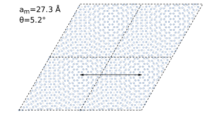
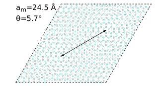
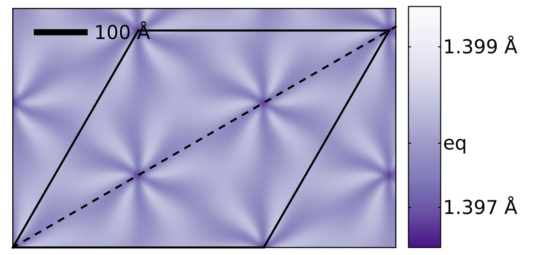
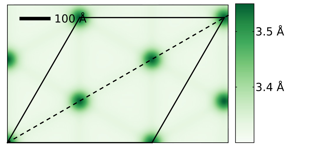
where is the relative orientation of two layers, with the distance between carbon atoms. In figure 1c,d is indicated by an arrow between the centers of the moiré patterns.
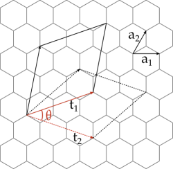
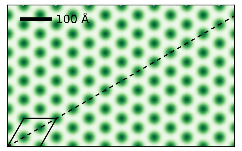
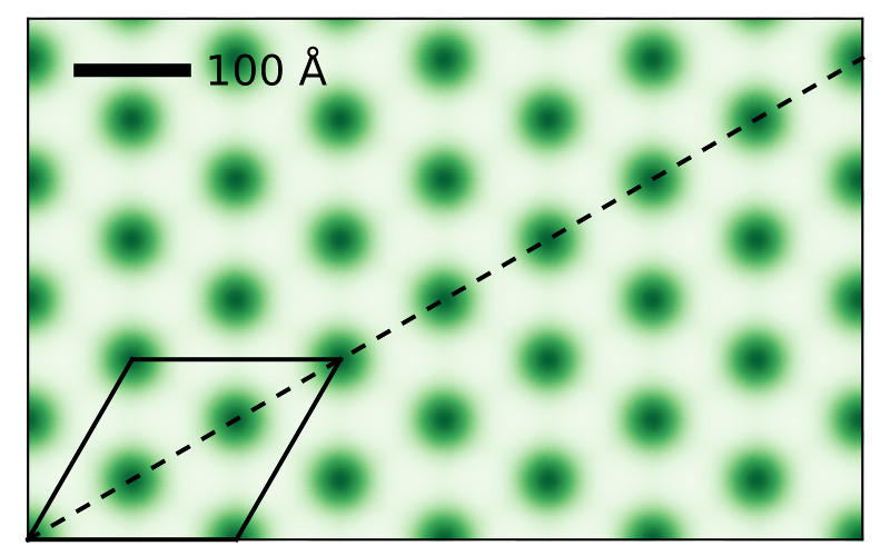
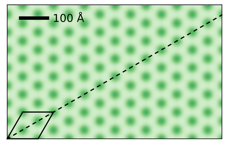
One may construct samples of twisted graphene satisfying periodic boundary conditions in the in-plane directions by identifying a common periodicity [25, 26, 23] in the two rotated layers as illustrated in figure 1a. For one layer, we define a supercell with a basis vector where and are the basis vectors of the graphene unit cell shown in figure 1a with and integers and . For the second layer, a cell with same size and rotated by an angle can be obtained by taking a basis vector . The common supercell is then obtained by rotating by the cell with basis vector and by the cell with basis vector . Each pair of n and m thus identifies a common supercell for two layers rotated by an angle given by
| (2) |
The supercell has sides of length
| (3) |
and contains atoms, with
| (4) |
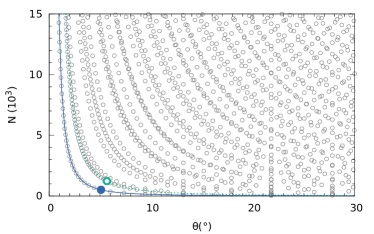
For small angles, this procedure quickly results in very large supercells, see figure 1b.
The size and shape of the moiré pattern does not change if the top layer shifts with respect to the bottom layer. In fact, a 60∘ rotation corresponds to a change from AA to AB stacking which can also be achieved by a translation. The symmetry of the hexagonal lattice combined with the translational freedom lead to a symmetry around .
The number of atoms in a single moiré pattern is given by [24]
| (5) |
This value also forms a lower bound for the number of atoms in the supercell since each supercell contains an integer number of moiré patterns. The values of on the minimum bound line in figure 1b correspond to supercells with , like the one in figure 1c. The next highlighted line in figure 1b corresponds to 3, for supercells with and three moiré patterns inside them (see figure 1d). The three moiré patterns in the supercell are not exactly equal due to the discreteness of the lattice, in the same way as a shift of the top layer leads to a moiré pattern that is not exactly the same as prior to the shift. In figure 1d one can see that the center of one moiré pattern is on an atom while the other is on the center of a hexagon. However, the differences between the moiré patterns are tiny and cannot be distinguished experimentally [27].
The size of the moiré pattern is thus determined by geometry, but its structure is determined by the atomic displacements that minimize the total energy. We have studied the effects of relaxation on the structure of the moiré patterns of twisted graphene on a graphite substrate and of double layer graphene. The interactions between atoms within the layer are given by the REBO potential [21] as implemented in the molecular dynamics code LAMMPS [28]. The interlayer interactions are given by the registry-dependent Kolmogorov-Crespi potential without the normals [23], scaled to match the equilibrium distance 1.3978 Å of the intralayer potential. The combination of these potentials has been shown to accurately reproduce the potential energy surface of the graphite substrate [29], although the corrugation is possibly underestimated [30].
Using the damped dynamics algorithm FIRE [31] we relax the atomic positions to their minimum energy configuration. As a model of graphene on graphite we consider a mobile layer of graphene on a rigid substrate whereas to model double layer graphene we allow atomic relaxations in both layers. For graphene on graphite we consider not only full relaxation in all directions but also a case where the interlayer distance is kept fixed at 3 Å. As this value is smaller than the equilibrium value (3.32 Å for AB stacking), the potential energy corrugation between layers is enhanced.
3 Graphene on graphite
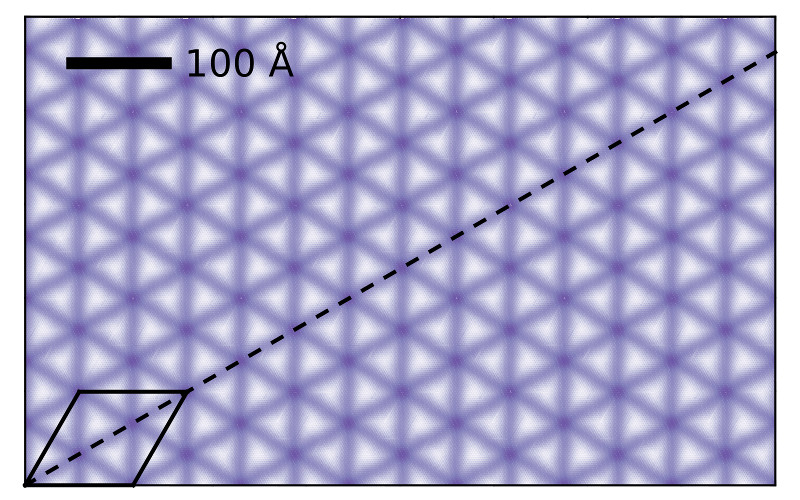
We first examine the case where the distance of the graphene layer to the rigid substrate is kept fixed and atoms are allowed to move only in the and directions. The AA areas become smaller while the AB stacked areas expand, as shown by the difference between figure 2a and figure 2b. This effect is achieved by a small rotation of each moiré pattern around the AA center as illustrated in figure 2c where we show the displacements from the positions prior to relaxation. For clarity we show the displacement for a sample with Å but similar vortex-like structures occur also for larger moiré patterns.


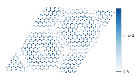
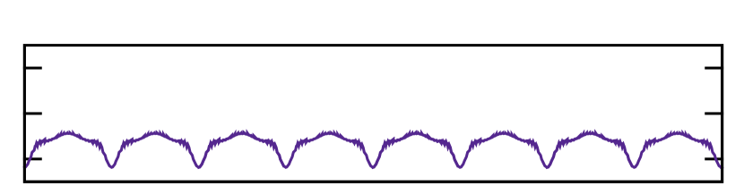
In figure 3 we show the distribution of bond lengths for decreasing angles. The rotational pattern in the displacements can also be observed in the bond lengths: the triangular pattern for and changes to a windmill shape for the larger moiré pattern with . We see that by reducing the angle, the modulation of the bond length changes from an almost sinusoidal behaviour to rather localized contraction close to the AA areas. The ‘windmill’ patterns appearing at small angles resemble those found in [19] as a function of the misfit energy, which in our case would correspond to an increasing penalty for AA stacking.
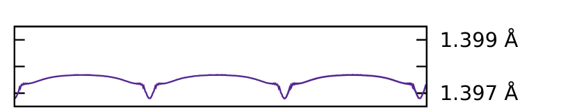
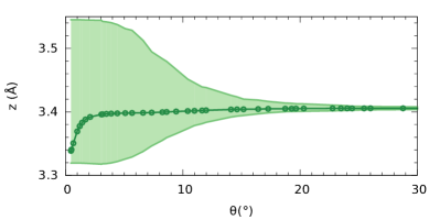
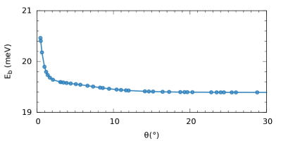
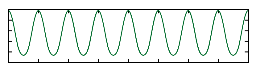
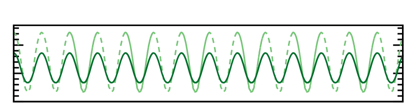
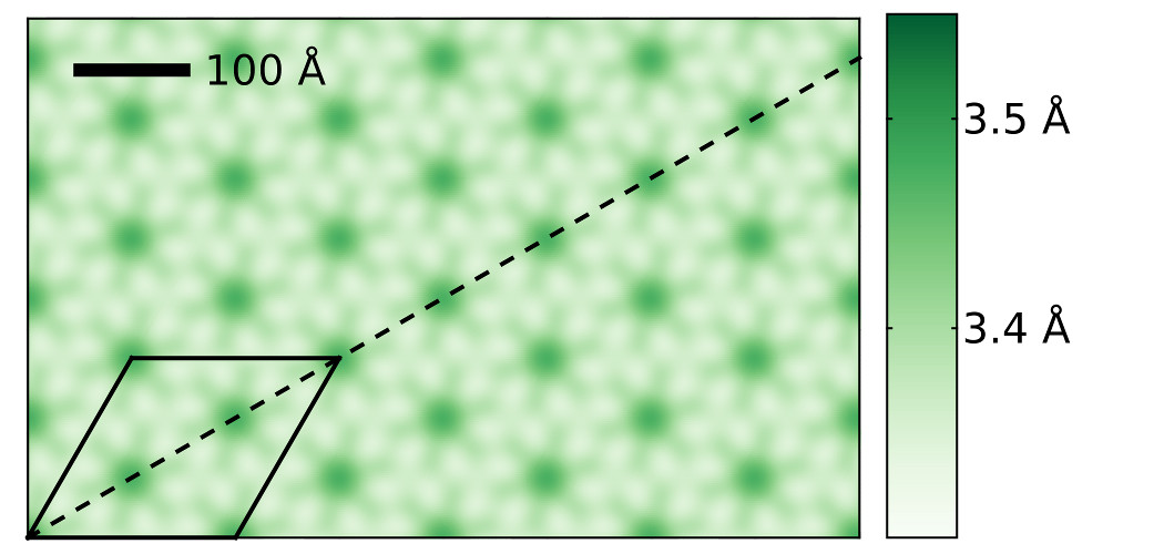
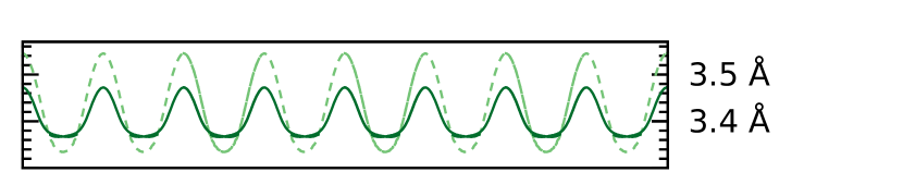
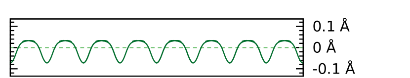
The distribution of bond lengths observed at fixed Å is very similar to those found when atoms are free to move in , although the differences are smaller than for Å, due to the increased distance and hence smaller corrugation. When the atoms are allowed to relax in the out-of-plane () direction, this is the main direction of the atomic displacements. In figure 4a the average distance to the substrate is shown, together with the minimum and maximum values. For , the graphene lies flat on the substrate. When decreases, the minimum and maximum values of are clearly different from the average. The spreading of agrees with the DFT calculations of [20] but the average value is not shown there. For , the minimum and maximum value of z stay constant at the equilibrium values of the AA and AB stacking, but the average distance to the substrate decreases, implying that the AB stacked areas grow. The binding energy , shown in figure 4b, stays constant for a large range of values as also found in [20]. Below , a range not reported in [20], we find that the binding energy increases significantly.
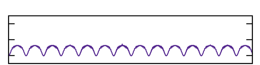
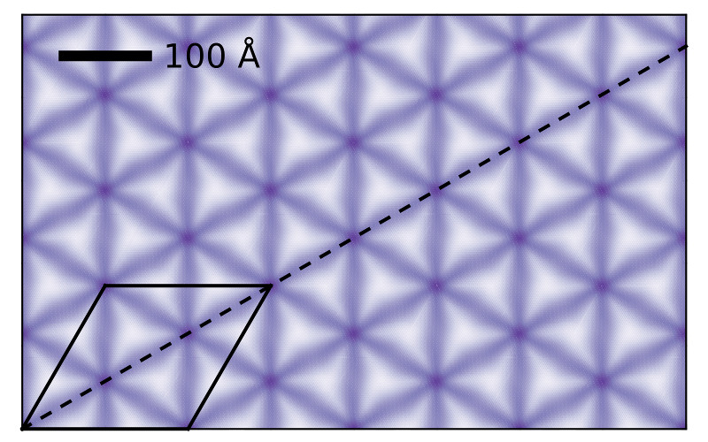
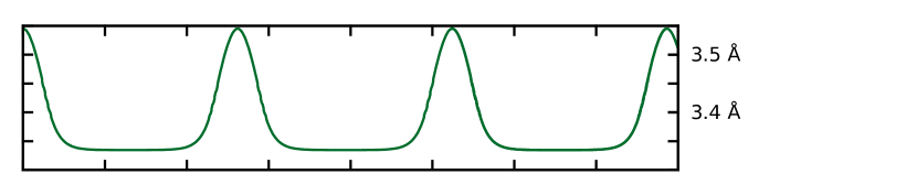
In figure 5 we show the distance from the substrate for three decreasing angles. In the panels showing the modulation along the cell diagonal, we see that the behaviour already found for the in-plane displacement is even more pronounced: for the modulation is roughly sinusoidal whereas for the ‘hot spots’ are very pronounced and separated by flat domains.
The main effects produced by structural deformations on the electronic properties of graphene are the modulation of the pseudo-electrostatic potential proportional to local uniform compression/dilatation and the appearance of a (pseudo)-vector potential with components proportional to the shear deformations [32, 33]:
| (6) |
where eV is the deformation potential for graphene, with the first neighbour interatomic distances in the deformed lattice, are hopping parameters in the deformed lattice, eV is their unperturbed value, is the electronic Grüneisen parameter. The resulting pseudo-magnetic field , which has an opposite sign for the two valleys K and K’, can be estimated as [33, 34]
| (7) |
where is a typical value of the shear deformation and is a typical size of the spatial variation of the deformation which we can estimate as .
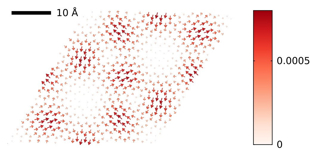
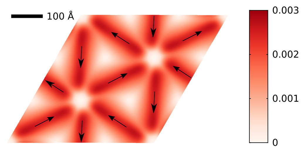
To estimate the strength of the pseudo magnetic field, we calculate the magnitude of the shear deformations from the first neighbour interatomic distances in the deformed lattice as
| (8) |
Taking the parameters from figure 6a,b we find in both cases of the order of 1 T, a value comparable to the one originating from ripples for graphene in SiO2 [34]. The straightforward experimental evidence of the existence of this field would be the suppression of weak localization effects [34]. For the smallest angle the field is much less homogeneous. We have indicated the main directions of the vector potential in the areas of largest shear deformation by arrows. One can see that the pattern is not trivial and, for instance, cannot be described as superposition of the field created by magnetic fluxes. The amplitude of the modulation of can be estimated to be a few meV.
4 Double layer graphene
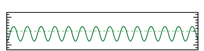
In order to model double layer graphene, we no longer consider a rigid substrate, but two graphene layers which are both free to move in all directions. Whereas for graphene on graphite all corrugation occurs within one layer, in the case of a double layer the corrugation is shared between two layers, as shown in figure 7. Furthermore we note that the deviation of the corrugation from the sinusoidal shape occurs for larger angles than in the case of graphene on graphite. Already at the behaviour is no longer sinusoidal and the relative deformation of the two layers seems to lead to a more complex pattern than for a single layer.
5 Conclusion
We have shown that the lattice deformations in graphene on graphite and double layer graphene for small misorientation angle become very different from the sinusoidal modulation commonly used in theoretical models, leading to a structure of ‘hot spots’ separated by roughly uniform domains. The relatively large out-of-plane deformation at the ‘hot spots’ should be observable by scanning probe microscopy. Despite the modest effect of relaxation on the in-plane modulation, we estimate that it could give rise to a quite strong pseudomagnetic field, affecting the electronic structure of graphene. It would be interesting to pursue this topic further and study more precisely the effect of atomic relaxation of slightly misaligned graphene layers on the electronic properties.
. We acknowledge interesting discussions with Yury Gornostyrev and Kostya Novoselov. This work is part of the research program of the Foundation for Fundamental Research on Matter (FOM), which is part of the Netherlands Organisation for Scientific Research (NWO). The research leading to these results has received funding from the European Union Seventh Framework Programme under grant agreement n°604391 Graphene Flagship. This work is supported in part by COST Action MP1303.
References
- [1] Geim A K and Grigorieva I V 2013 Nature 499 419–425
- [2] Britnell L, Gorbachev R V, Jalil R, Belle B D, Schedin F, Mishchenko A, Georgiou T, Katsnelson M I, Eaves L, Morozov S V et al. 2012 Science 335 947–950
- [3] Yankowitz M, Xue J, Cormode D, Sanchez-Yamagishi J D, Watanabe K, Taniguchi T, Jarillo-Herrero P, Jacquod P and LeRoy B J 2012 Nature Phys. 8 382–386
- [4] Ponomarenko L A, Gorbachev R V, Yu G L, Elias D C, Jalil R, Patel A A, Mishchenko A, Mayorov A S, Woods C R, Wallbank J R, Mucha-Kruczynski M, Piot B A, Potemski M, Grigorieva I V, Novoselov K S, Guinea F, Fal’ko V I and Geim A K 2013 Nature 497 594–597
- [5] Dean C, Wang L, Maher P, Forsythe C, Ghahari F, Gao Y, Katoch J, Ishigami M, Moon P, Koshino M, Taniguchi T, Watanabe K, Shepard K L, Hone J and Kim P 2013 Nature 497 598–602
- [6] Hunt B, Sanchez-Yamagishi J D, Young A F, Yankowitz M, LeRoy B J, Watanabe K, Taniguchi T, Moon P, Koshino M, Jarillo-Herrero P and Ashoori R C 2013 Science 340 1427–1430
- [7] Woods C R, Britnell L, Eckmann A, Ma R, Lu J, Guo H M, Lin X, Yu G L, Cao Y, Gorbachev R V et al. 2014 Nature physics 10 451–456
- [8] van Wijk M M, Schuring A, Katsnelson M I and Fasolino A 2014 Phys. Rev. Lett. 113 135504
- [9] Dienwiebel M, Verhoeven G S, Pradeep N, Frenken J W, Heimberg J A and Zandbergen H W 2004 Phys. Rev. Lett. 92 126101
- [10] Li G, Luican A, Dos Santos J M B L, Neto A H C, Reina A, Kong J and Andrei E Y 2010 Nature Phys. 6 109–113
- [11] Luican A, Li G, Reina A, Kong J, Nair R R, Novoselov K S, Geim A K and Andrei E Y 2011 Phys. Rev. Lett. 106 126802
- [12] Bistritzer R and MacDonald A H 2011 Phys. Rev. B 84 035440
- [13] Trambly de Laissardiere G, Mayou D and Magaud L 2010 Nano Lett. 10 804–808
- [14] Schmidt H, Rode J C, Smirnov D and Haug R J 2014 Nature Comm. 5
- [15] Chen Y, Meng L, Zhao W, Liang Z, Wu X, Nan H, Wu Z, Huang S, Sun L, Wang J and Ni Z 2014 Phys. Chem. Chem. Phys. 16 21682–21687
- [16] Wallbank J R, Mucha-Kruczynski M, Chen X and Fal’ko V I 2014 arXiv:1411.1235
- [17] Frank F C and Van der Merwe J H 1949 Proc. R. Soc. Lond. Ser. A 198 205–216
- [18] Bak P 1982 Rep. Prog. in Phys. 45 587–629
- [19] Snyman J A and Snyman H C 1981 Surf. Sci. 105 357–376
- [20] Uchida K, Furuya S, Iwata J I and Oshiyama A 2014 Phys. Rev. B 90 155451
- [21] Brenner D W, Shenderova O A, Harrison J A, Stuart S J, Ni B and Sinnott S B 2002 J. Phys.: Cond. Mat. 14 783
- [22] Los J H, Ghiringhelli L M, Meijer E J and Fasolino A 2005 Phys. Rev. B 72 214102
- [23] Kolmogorov A N and Crespi V H 2005 Phys. Rev. B 71 235415
- [24] Hermann K 2012 J. Phys.: Cond. Mat. 24 314210
- [25] Shallcross S, Sharma S, Kandelaki E and Pankratov O A 2010 Phys. Rev. B 81 165105
- [26] Savini G, Dappe Y, Öberg S, Charlier J C, Katsnelson M I and Fasolino A 2011 Carbon 49 62–69
- [27] Yıldız D, Şen H Ş, Gülseren O and Gürlü O 2015 arXiv:1502.00869
- [28] Plimpton S 1995 J. Comput. Phys. 117 1–19
- [29] Reguzzoni M, Fasolino A, Molinari E and Righi M C 2012 Phys. Rev. B 86 245434
- [30] Lebedeva I V, Knizhnik A A, Popov A M, Lozovik Y E and Potapkin B V 2011 Phys. Chem. Chem. Phys. 13 5687–5695
- [31] Bitzek E, Koskinen P, Gähler F, Moseler M and Gumbsch P 2006 Phys. Rev. Lett. 97 170201
- [32] Vozmediano M A H, Katsnelson M I and Guinea F 2010 Phys. Rep. 496 109–148
- [33] Katsnelson M I 2012 Graphene: carbon in two dimensions (Cambridge University Press)
- [34] Morozov S V, Novoselov K S, Katsnelson M I, Schedin F, Ponomarenko L A, Jiang D and Geim A K 2006 Phys. Rev. Lett. 97 016801