Belle II Silicon Vertex Detector
Abstract
The Belle II experiment at the SuperKEKB collider in Japan is designed to indirectly probe new physics using approximately times the data recorded by its predecessor. An accurate determination of the decay-point position of subatomic particles such as beauty and charm hadrons as well as a precise measurement of low-momentum charged particles will play a key role in this pursuit. These will be accomplished by an inner tracking device comprising two layers of pixelated silicon detector and four layers of silicon vertex detector based on double-sided microstrip sensors. We describe herein the design, prototyping and construction efforts of the Belle-II silicon vertex detector.
keywords:
Belle II , SVD , Origami assembly , APV25 chip , CO2 coolingPACS:
29.40.Gx , 29.40.Wk , 07.50.Qx1 Introduction
The discovery of a new particle, which is consistent with the Higgs boson within the current experimental uncertainties, by the ATLAS [1] and CMS [2] experiments at the LHC seems to complete the story of the standard model. The focus is now geared towards deciphering the next fundamental layer of physics, often referred to as “new physics”, as the standard model has several shortcomings. For instance, it does not have a suitable dark-matter candidate, nor can it fully account for the observed matter-antimatter asymmetry in universe.
As a next-generation flavor experiment, Belle II [3] at the SuperKEKB collider [4] is expected to play a pivotal role in the above pursuit. Using a huge sample of collision data recorded at various resonances, about times that of its predecessor experiment (Belle [5]), it will indirectly probe new physics at an unprecedented level. Measurements of charge-parity violation asymmetry in the decays of beauty and charm hadrons constitute a key experimental approach for Belle II. The studies hinge on an accurate determination of decay-point positions of these hadrons as well as a precise measurement of low-momentum charged particles. These important tasks are accomplished by a sophisticated inner tracking device comprising two layers of pixelated silicon detector (PXD) and four layers of silicon vertex detector (SVD) based on double-sided microstrip sensors.
We report herein the design, prototyping and construction efforts of the Belle-II SVD. Details on the PXD can be found at Ref. [6].
2 Silicon Vertex Detector
The PXD and SVD are the two innermost subdetectors of the Belle II experiment. They nicely complement each other in providing information of excellent spatial granularity and timing resolution. The resulting impact parameter resolution improves by a factor of two compared to Belle, from 40 down to 20 m [3]. Furthermore, the reconstruction efficiency of low-momentum particles and relatively long-lived particles such as mesons is improved, thanks to the extended outermost SVD layer. The radii of the inner two PXD layers (Layer 1 and 2) are and mm, while the radii of the outer four SVD layers (Layer 3 through 6) are , , , and mm. In comparison, Belle had the outermost SVD layer at a radius of mm [7].
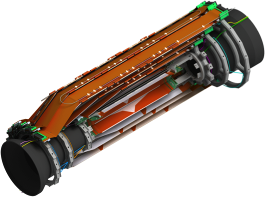
Figure 1 shows a cut-off view of the SVD. Its L3, L4, L5, and L6 (L stands for Layer) are respectively composed of , , , and modules or ‘ladders’ with a polar-angle coverage of . The asymmetry reflects the forward boost of the center-of-mass system arising due to a difference in energies ( on GeV) of the colliding and beams. The L3 ladders are straight in shape, while those for L4-6 exhibit a slanted structure in the forward side. The corresponding slant angles are , and . The idea behind this lantern-like layout is to reduce the material budget and number of readout channels without compromising the performance. Clearly, these benefits come at the cost of a fairly complex mechanical structure.
3 Sensors and Readout ASIC
Three types of double-sided silicon microstrip detectors (DSSDs) are used in the SVD, all having the same length of 12.3 cm and thickness of 300 or 320 m. The large rectangular DSSDs are cm wide and fully utilize the available space on a 6-inch wafer. A smaller width ( cm) is chosen for L3 to ensure that the DSSDs are aranged in a circular fashion around the PXD. The width of the trapezoidal DSSDs in the forward part ranges between to cm. Table 1 lists the specifications of various DSSDs used in the SVD.
| Type | # strip | # strip | Strip pitch | Strip pitch | Active area |
|---|---|---|---|---|---|
| p-side | n-side | p-side (m) | n-side (m) | () | |
| Small | |||||
| Large | |||||
| Trape. | - |
The longer strips on the p-side are placed along the axis (parallel to the beam direction) and the shorter strips on the n-side are located on the transverse - plane. The p-side of the L4-6 DSSDs faces the beam pipe, while the L3 DSSDs are oppositely arranged. Both small and large rectangular DSSDs are fabricated by Hamamatsu Photonics in Japan, and the trapezoidal ones by Micron Semiconductor in the UK.
To cope with the high particle rates expected at Belle II, the DSSDs require fast readout electronics with a short integration (shaping) time. A pipeline is also necessary to allow a dead-time free data taking. Furthermore, a radiation tolerance up to kGy is desirable. The APV25 readout chip [8], originally developed for CMS, is found to satisfy all these requirements. It has a shaping time of ns, compared to ns of the VA1TA chip used in Belle, a pipeline depth of cells, and a nominal clock speed of MHz. These chips are fabricated using a m CMOS process and can withstand a radiation dose of over MGy.
Due to faster shaping of the APV25 chip compared to VA1TA, a smaller input capacitance is required for the amplifier to retain signal-to-noise ratio. This also means that concatenations of several DSSDs, as was done for Belle, are simply prohibitive necessitating the need to place the readout ASIC as close to the DSSD as possible. These conflicting requirements are met by the so-called “origami” chip-on-sensor design [9].
4 Origami Chip-on-sensor Design
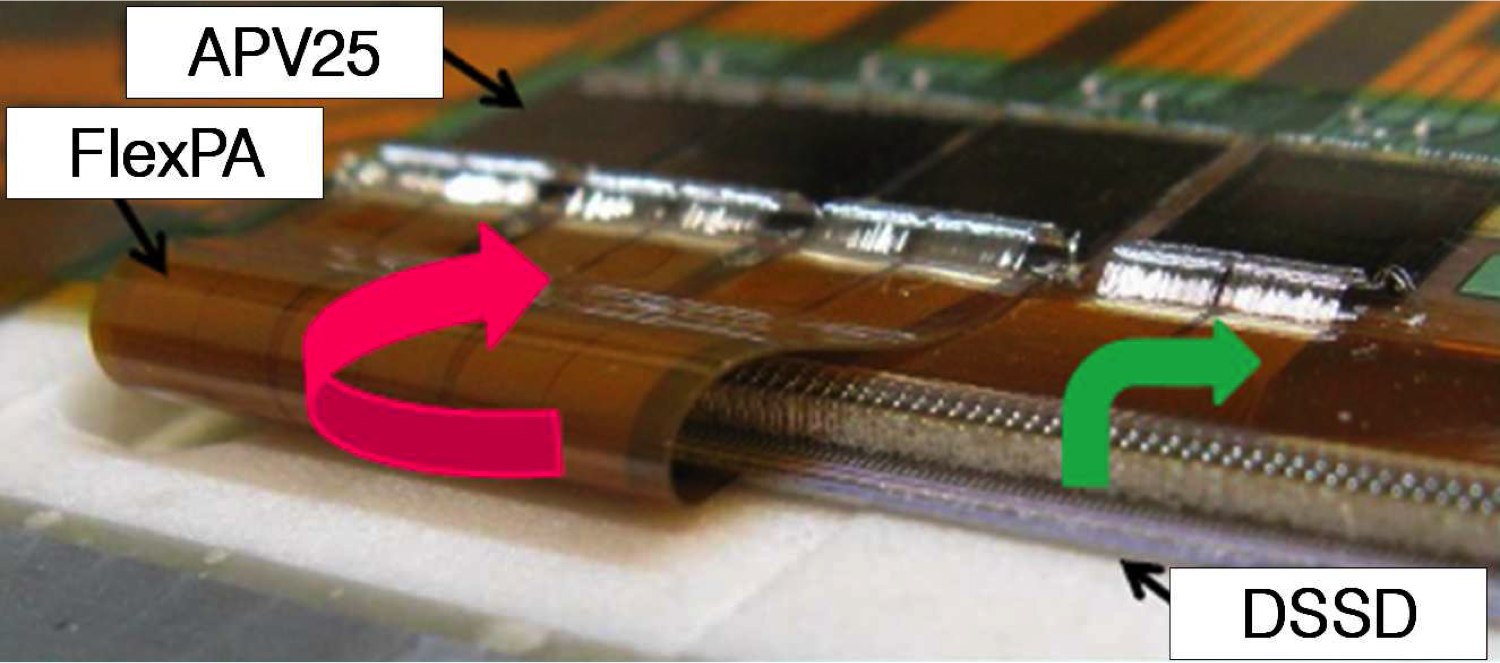
The full L3 ladder, and the forward and backward DSSDs in L4-6 adopt an edge-side readout scheme with fanouts, similar to Belle. On the other hand, the central DSSDs (one, two, and three for an L4, L5, and L6 ladder, respectively) rely on the origami concept. This novel scheme helps minimize the distance between the DSSD and the readout electronics, which in turn reduces the capacitive noise. The origami is a three-layer flexible fanout circuit (FlexPA) made of polymide. It has ten APV25 chips for reading out the sensors. Table 2 describes the number of ladders for each SVD layer, the number of DSSDs and origamis per ladder, and the number of APV25 chips per DSSD.
| Layer | Ladders | DSSDs/ladder | Origamis/ladder | APVs/DSSD |
|---|---|---|---|---|
| L3 | 7 | 2 | 0 | 12 |
| L4 | 10 | 3 | 1 | 10 |
| L5 | 12 | 4 | 2 | 10 |
| L6 | 16 | 5 | 3 | 10 |
We need three different kinds of origami FlexPA designs depending on the SVD layer: (backward), ce (central), and (forward). All three of them are electrically equivalent differing only in the length of the tail part, or in the outer shape in case of origami , which is only used in L6. Between the FlexPA and DSSDs, a mm thick sheet of light-weight styrofoam (Airex [10]) is inserted. This sheet provides both thermal and electrical insulation to minimize the heat transfer from the chips to the DSSDs and to avoid signal cross-talk. The APV25 chips are thinned down to 100 m for the material budget reduction, and are glued to the origami FlexPA by a thin layer of conductive adhesive. The n-side strips of a DSSD are directly connected to the chips by wire-bonding and a small fanout circuit. Those of the p-side are attached by two flexible fanout circuits, which are bent around the edge of the DSSD and glued onto the origami FlexPA in front of the APV25 chips. A gluing robot is used to dispense the glue, while an ultrasonic wedge bonder used for wire-bonding. Figure 2 shows the key feature of the origami concept.
5 Assembly Procedure
The ladder assembly procedure [11] is complicated and requires several kinds of jigs for each operation involved. The main purpose of these jigs is to ensure a precise alignment of the DSSDs during assembly. The total number of jigs required is different for each layer, being the maximum for L6.
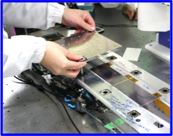
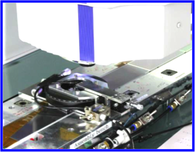
For the ladder assembly, we align the central DSSD(s) with the p-side at top, glue two fanout circuits on it, and perform wire-bonding between the readout and fanout circuit pads. We then flip the DSSD and place it on the assembly bench. At this stage, we pickup the forward and backward subassemblies from the multipurpose chuck and place them on the assembly bench. We use a precision three-dimensional coordinate measuring machine (CMM) to align the sensors within a tolerance of 10 m. Each ladder is supported by two ribs made of carbon-fiber reinforced Airex foam. The rib structure is very light but extremely stiff. We pick up the forward and backward subassemblies from the assembly bench, and glue them on the ribs. While assembling the central DSSD we first glue the Airex on the sensor, glue the origami module on the Airex, and then perform wirebonding. The pick-up and placing of the sensors and flex circuits are accomplished via vacuum chucking. At the end, we place the plastic clips for holding the cooling pipe (see below). Figure 3 illustrates a part of the ladder assembly procedure.
On top of all APVs, we place a sheet of glass fiber and silicone rubber composite (Keratherm [12]) that is electrically isolated but thermally conductive. The SVD power dissipation per active area is estimated to be 60.7 mW/cm2. The APV25 chips are cooled down to C with two-phase CO2 flowing inside a thin -mm diameter pipe that is placed on Keratherm. This cooling has two major advantages: a) it can withstand large amount of radiation and b) it exhibits an excellent thermomechanical behavior. Both the PXD and SVD system share a common volume, filled with dry nitrogen gas to maintain a stable temperature and low dew point for avoiding condensation. The average material budget for one ladder including ribs, DSSDs, electronics and cooling is about of a radiation length.
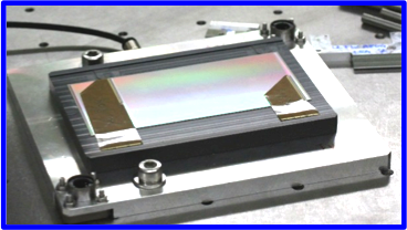
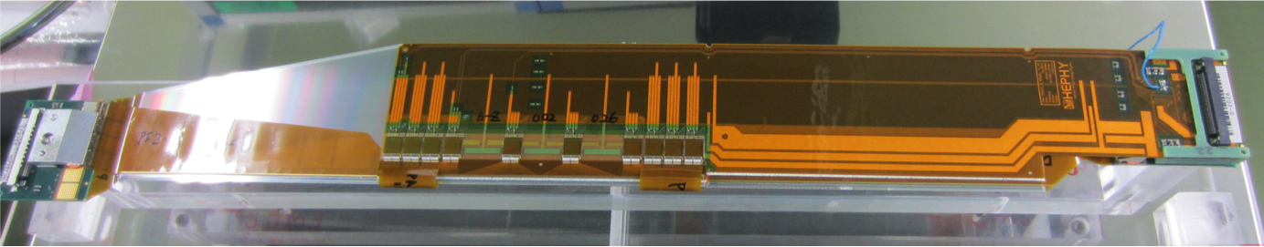
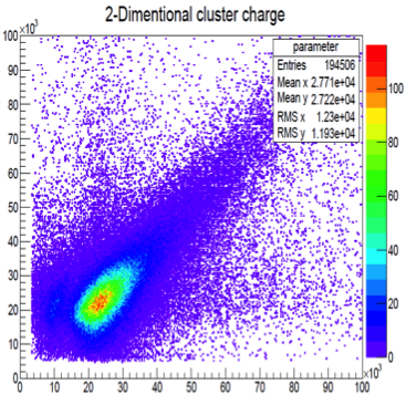
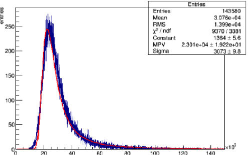
The construction workflow is split among several sites. The forward and backward subassemblies are produced at INFN Pisa and later shipped to other assembly sites: L4 (TIFR), L5 (HEPHY), and L6 (IPMU). The L3 assembly is performed by the Melbourne group. The R&D for the ladder assembly procedure is now over, and each site has assembled a number of mechanical prototypes as well as one or two electrically working ladders. The latter have been tested with a -ray source or laser to assess the overall performance and potential defects of the sensors. We present an L4 mechanical prototype in Figure 4. Results of the source measurement performed on an electrically working L5 ladder are shown in Figure 5.
6 Backend Electronics
Figure 6 shows an overview of the whole SVD readout system [13]. The analog signals from the APV25 chips are transmitted to flash analog-to-digital converter (FADC) boards via repeater boards. Each FADC board can receive up to 48 APV25 analog outputs, and performs the analog to digital conversion for obtaining digitized signals. The digitized signals are decoded and further processed on an FPGA, and propagated to a finesse transmitter board (FTB). The FTB sends the data to the common pipelined platform for electronics readout (COPPER), which is the Belle II DAQ interface, through an optical cable using a unified high-speed serial protocol (belle2link). In parallel, the FTB also transmits a replica output to the PXD data acquistion system using an Aurora link. The COPPER board performs further data processing and sends the data for storage via the high-level trigger (HLT) system.
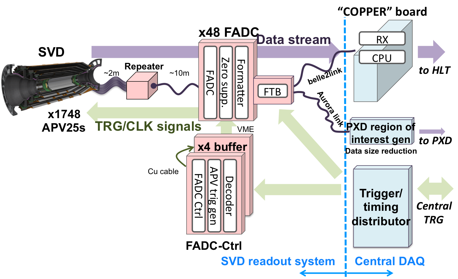
A total of 48 FADC boards and 48 FTBs will be employed across Belle II. All the components in the SVD readout system are being developed while prototypes were successfully produced and tested.
7 Beam Test Results
A test of the complete PXD+SVD readout chain was performed [14] using the electron beam at DESY. The beam energy was 2 to 6 GeV and 1 T of magnetic field was applied perpendicular to the beam line. The set-up included four SVD test modules, with one large rectangular DSSD in each, and one PXD module in a light-tight box, FADC and FTB boards, CO2 cooling, slow control and environmental sensors based on optical fiber sensors. Several aspects were checked. We find the SVD cluster hit efficiency to be above for tracks within the fiducial volume. Further, we confirm that the common mode correction and zero suppression schemes do not deteriorate the SVD hit efficiency.
8 Conclusions
In summary, the KEKB machine and Belle experiment are being upgraded to SuperKEKB and Belle II with a goal to indirectly probe new physics, in which the SVD will play a key role. We have developed a robust assembly procedure for the SVD ladder modules after extensive R&D. This includes the production of dedicated jigs, their fine-tuning and handling, glue spread control, and wire-bonding parameter tuning. The most innovative aspect among all has been the origami chip-on-sensor scheme that enables an excellent signal-to-noise ratio by reducing the capacitive noise. The assembly procedure is found to be reproducible allowing us to consistently assemble the ladders with an acceptable mechanical offset and good electrical quality.
The full-scale production of SVD ladders will start at the beginning of 2016, which will be followed by commissioning in mid-2017. The first physics run with both PXD and SVD in will be towards the end of 2018.
Acknowledgements
We congratulate the organizers for a well organized conference and are grateful to colleagues those have helped us in preparing these proceedings. The research leading to these results has received funding from the European Commission under the FP7 Research Infrastructures project AIDA, grant agreement no. 262025.
References
- [1] ATLAS Collaboration, Phys. Lett. B 716 (2012) 1.
- [2] CMS Collaboration, Phys. Lett. B 716 (2012) 30.
- [3] T. Abe et al. (Belle II Collaboration), arXiv:1011.0352 [physics.ins-det].
- [4] Y. Ohnisi et al., PTEP 2013, 03A011.
- [5] J. Brodzicka et al. (for the Belle Collaboration), PTEP 2012, 04D001.
- [6] H.-G. Moser, in these proceedings.
- [7] Z. Natkaniec et al. (Belle SVD2 Group), Nucl. Instrum. Methods Phys. Res., Sect. A 560 (2006) 1.
- [8] M. French et al., Nucl. Instrum. Methods Phys. Res., Sect. A 466 (2001) 359.
- [9] C. Irmler et al., JINST 8 (2013) C01014.
- [10] Airex AG (Switzerland), http://www.airexag.ch.
- [11] C. Irmler et al., JINST 11 (2016) C01087.
- [12] Kerafol GmBH (Germany), http://www.kerafol.com.
- [13] K. Nakamura et al., PoS TIPP 2014 (2014) 198.
- [14] M. Friedl et al., JINST 9 (2014) C12005.