Generalized circuit model for coupled plasmonic systems
Felix Benz,1 Bart de Nijs,1 Christos Tserkezis,2 Rohit Chikkaraddy,1 Daniel O. Sigle,1 Laurynas Pukenas,3 Stephen D. Evans,3 Javier Aizpurua,2 and Jeremy J. Baumberg1,∗
1NanoPhotonics Centre, Cavendish Laboratory, JJ Thompson Ave, University of Cambridge, Cambridge, CB3 0HE, UK
2Donostia International Physics Center (DIPC) and Centro de Física de Materiales, Centro Mixto CSIC-UPV/EHU, Paseo Manuel Lardizabal 4, 20018 Donostia/San Sebastián, Spain
3Molecular and Nanoscale Physics, School of Physics and Astronomy, University of Leeds, Leeds, LS2 9JT, UK
∗jjb12@cam.ac.uk
Abstract
We develop an analytic circuit model for coupled plasmonic dimers separated by small gaps that provides a complete account of the optical resonance wavelength. Using a suitable equivalent circuit, it shows how partially conducting links can be treated and provides quantitative agreement with both experiment and full electromagnetic simulations. The model highlights how in the conducting regime, the kinetic inductance of the linkers set the spectral blue-shifts of the coupled plasmon.
OCIS codes: (250.5403) Plasmonics; (240.6680) Surface plasmons; (160.4236) Nanomaterials; (160.3918) Metamaterials.
References and links
- [1] J. Homola, Surface plasmon resonance sensors for detection of chemical and biological species, Chem. Rev. 108, 462–493 (2008).
- [2] R.W. Taylor, F. Benz, D.O. Sigle, R.W. Bowman, P. Bao, J.S. Roth, G.R. Heath, S.D. Evans, and J.J. Baumberg, Watching individual molecules flex within lipid membranes using SERS, Sci. Rep. 4, 5940 (2014).
- [3] G. Di Martino, Y. Sonnefraud, M.S. Tame, S. Kéna-Cohen, F. Dieleman, Ş.K. Özdemir, M.S. Kim, and S.A. Maier, Observation of quantum interference in the plasmonic Hong-Ou-Mandel effect, Phys. Rev. Appl. 1, 034004 (2014).
- [4] G. Di Martino, Y. Sonnefraud, S. Kéna-Cohen, M. Tame, Ş.K. Özdemir, M.S. Kim, and S.A. Maier, Quantum statistics of surface plasmon polaritons in metallic stripe waveguides, Nano Lett. 12, 2504–2508 (2012).
- [5] H. Itoh, K. Naka, and Y. Chujo, Synthesis of dold nanoparticles modified with ionic liquid based on the imidazolium cation, J. Am. Chem. Soc. 126, 3026–3027 (2004).
- [6] F. J. García de Abajo and J. Aizpurua, Numerical simulation of electron energy loss near inhomogeneous dielectrics, Phys. Rev. B 56, 15873–15884 (1997).
- [7] R. Esteban, A.G. Borisov, P. Nordlander, and J. Aizpurua, Bridging quantum and classical plasmonics with a quantum-corrected model, Nat. Commun. 3, 825 (2012).
- [8] A. Salandrino and N. Engheta, Far-field subdiffraction optical microscopy using metamaterial crystals: Theory and simulations, Phys. Rev. B 74, 075103 (2006).
- [9] M. Pelton, J. Aizpurua, and G. Bryant, Metal-nanoparticle plasmonics, Laser Photonics Rev. 2, 136–159 (2008).
- [10] A. Taflove and S.C. Hagness, Computational electrodynamics: the finite-difference time-domain method, (Artech House, 2005).
- [11] A. Dhawan, S.J. Norton, M.D. Gerhold, and T. Vo-Dinh, Comparison of FDTD numerical computationsand analytical multipole expansion method for plasmonics-active nanosphere dimers, Opt. Express 17, 9688–9703 (2009).
- [12] R. Trivedi, A. Thomas, and A. Dhawan, Full-wave electromagentic analysis of a plasmonic nanoparticle separated from a plasmonic film by a thin spacer layer, Opt. Express 22, 19970 (2014).
- [13] I.E. Mazets, Polarization of two close metal spheres in an external homogeneous electric field, Tech. Phys. 45, 1238–1240 (2000).
- [14] N. Engheta, A. Salandrino, and A. Alú, Circuit elements at optical frequencies: nanoinductors, nanocapacitors, and nanoresistors, Phys. Rev. Lett. 95, 095504 (2005).
- [15] N. Engheta, Circuits with light at nanoscales: optical nanocircuits inspired by metamaterials, Science 317, 1698–1702 (2007).
- [16] N. Liu, F. Wen, Y. Zhao, Y. Wang, P. Nordlander, N.J. Halas, and A. Alú, Individual nanoantennas loaded with three-dimensional optical nanocircuits, Nano Lett. 13, 142–147 (2013).
- [17] J. Shi, F. Monticone, S. Elias, Y. Wu, D. Ratchford, X. Li, and A. Alú, Modular assembly of optical nanocircuits, Nat. Commun. 5, (2014).
- [18] V. Myroshnychenko, J. Rodríguez-Fernández, I. Pastoriza-Santos, A.M. Funston, C. Novo, P. Mulvaney, L.M. Liz-Marzán and F. Javier García de Abajo, Modelling the optical response of gold nanoparticles, Chem. Soc. Rev. 37, 1792–1805 (2008).
- [19] A.K. Sarychev and V.M. Shalaev, Electromagnetic field fluctuations and optical nonlinearities in metal-dielectric composites, Phys. Rep. 335, 275–371 (2000).
- [20] F. Benz, B. de Nijs, C. Tserkezis, R. Chikkaraddy, D.O. Sigle, L. Pukenas, S.D. Evans, J. Aizpurua, and J.J. Baumberg, Data for Generalized circuit model for coupled plasmonic systems, DSpace@Cambridge (2015), https://www.repository.cam.ac.uk/handle/1810/252428.
- [21] P.K. Jain, W. Huang, and M.A. El-Sayed, On the universal scaling behavior of the distance decay of plasmon coupling in metal nanoparticle pairs: a plasmon euler equation, Nano Lett. 7, 2080–2088 (2007).
- [22] C. Sönnichsen, B.M. Reinhard, J. Liphardt, and A.P. Alivisatos, A molecular ruler based on plasmon coupling of single gold and silver nanoparticles, Nat. Biotechnol. 23, 741–745 (2005).
- [23] C. Cirací, R.T. Hill, J.J. Mock, Y. Urzhumov, A.I. Fernández-Domínguez, S.A. Maier, J.B. Pendry, A. Chilkoti, and D.R. Smith, Probing the ultimate limits of plasmonic enhancement, Science 337, 1072–1074 (2012).
- [24] F. Benz, C. Tserkezis, L.O. Herrmann, B. de Nijs, A. Sanders, D.O. Sigle, L. Pukenas, S.D. Evans, J. Aizpurua, and J.J. Baumberg, Nanooptics of Molecular-Shunted Plasmonic Nanojunctions, Nano Lett. 15, 669–674 (2015).
- [25] K.J. Savage, M.M. Hawkeye, R. Esteban, A.G. Borisov, J. Aizpurua, and J.J. Baumberg, Revealing the quantum regime in tunnelling plasmonics, Nature 491, 574–577 (2012).
- [26] J.A. Scholl, A. García-Etxarri, A.L. Koh, and J.A. Dionne, Observation of quantum tunneling between two plasmonic nanoparticles, Nano Lett. 13, 564–569 (2013).
- [27] O. Pérez-González, N. Zabala, A.G. Borisov, N.J. Halas, P. Nordlander, and J. Aizpurua, Optical spectroscopy of conductive junctions in plasmonic cavities, Nano Lett. 10, 3090–3095 (2010).
- [28] P. Nordlander and E. Prodan, Plasmon hybridization in nanoparticles near metallic surfaces, Nano Lett. 4, 2209–2213 (2004).
- [29] S. Hudlet, M. Saint Jean, C. Guthmann, and J. Berger, Evaluation of the capacitive force between an atomic force microscopy tip and a metallic surface, Eur. Phys. J. B 2, 5–10 (1998).
- [30] F.J. García de Abajo and A. Howie, Retarded field calculation of electron energy loss in inhomogeneous dielectrics, Phys. Rev. B 65, 115418 (2002).
- [31] M. Hegner, P. Wagner, and G. Semenza, Ultralarge atomically flat template-stripped Au surfaces for scanning probe microscopy, Surf. Sci. 291, 39–46 (1993).
- [32] B. de Nijs, R.W. Bowman, L.O. Herrmann, F. Benz, S.J. Barrow, J. Mertens, D.O. Sigle, R. Chikkaraddy, A. Eiden, A. Ferrari, O.A. Scherman, and J.J. Baumberg, Unfolding the contents of sub-nm plasmonic gaps using normalising plasmon resonance spectroscopy, Faraday Discuss. 178, 185–193 (2015).
- [33] M. Staffaroni, J. Conway, S. Vedantam, J. Tang, and E. Yablonovitch, Circuit analysis in metal-optics, Photonics Nanostructures - Fundam. Appl. 10, 166–176 (2012).
- [34] J.P. Folkers, P.E. Laibinis, G.M. Whitesides, Self-assembled monolayers of alkanethiols on gold: comparisons of monolayers containing mixtures of short- and long-chain constituents with methyl and hydroxymethyl terminal groups. Langmuir 8, 1330–1341 (1992).
- [35] C.D. Bain, E.B. Troughton, Y.T. Tao, J. Evall, G.M. Whitesides, R.G. Nuzzo, Formation of monolayer films by the spontaneous assembly of organic thiols from solution onto gold. J. Am. Chem. Soc. 111, 321–335 (1989).
1 Introduction
Plasmonic nanostructures are at the heart of many research fields ranging from biological applications [1, 2] to quantum information processing [3, 4]. In recent years significant progress has been made in both the chemical preparation of noble-metal nanostructures [5] and in simulation tools to model them [6, 7, 8, 9, 10]. However, few attempts have been made to develop a comprehensive analytical model [11, 12] that could facilitate direct validation of experimental results and yield parameters that can guide the implementation of full electromagnetic simulations. Most analytical approaches approximate Maxwell’s equations and are limited to specific geometries, like large gap separations [13]. A promising alternative is to treat any nanoplasmonic system as a high frequency circuit composed of capacitors, inductors, and resistors [14, 15, 16, 17]. Such a circuit model is extremely versatile as generalized equations for the resonance condition can be obtained, and their dependence on the geometry of the nanostructure understood explicitly. Here we use this circuit approach to develop a simple analytical expression for two coupled plasmonic systems in close proximity. Surprisingly this has been absent until now, despite its extreme utility, because a number of subtle effects need to be considered. Our model is capable of describing both insulating and conductive gaps and applicable to arbitrary coupled plasmonic systems. We stress that such models are extremely useful to guide experiments, as electromagnetic simulation tools do not give direct insights (like those shown here) or scaling rules on the details of the nano-geometry. In the ultrasmall gap regime used here (and of strong interest for experiments), we show these models are accurate enough to be highly effective.
In this work we first review the circuit model for single nanoparticles, and show how to effectively account for nanoparticle size. We then show the full model for coupled plasmonics components when the gap between them is insulating, and when the gap has a finite conductance. We then show the origin of the scaling in the resonance coupled wavelength arising from the inductance of the gap region, producing a simple estimate for the blueshifts observed.
2 Single particles
We start from the description of a single spherical nanoparticle, which is well characterized by an LC circuit that has been shown to be the exact solution to Maxwell’s equations. Engetha et al.[14] have determined the impedance contributions of the fringing field and the sphere with nanoparticle radius , frequency , gold permittivity , vacuum permittivity , and the capacitance due to the fringing field . The resonance wavelength can be determined by , which yields the well-known resonance condition in the electrostatic case for a plasmonic nanoparticle . Here, throughout we use a Drude model for the dielectric function of gold:
| (1) |
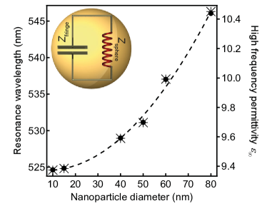
This yields the single particle resonance frequency, . The plasma frequency and wavelength ( and respectively), and the background high frequency permittivity () are material parameters which should not depend on nanoparticle size. However, electrodynamical effects, beyond the electrostatic approximation, lead to a weak particle size dependence of the resonance wavelength. There are several ways of correcting the resonance condition due to retardation [18, 19], however, a relatively simple phenomenological way to account for this is to assume that depends slightly on the nanoparticle size. The resonance wavelength of different gold nanoparticle sizes in water (permittivity ) from extinction spectroscopy (Fig. 1) provides estimated values for using together with Eq. (1), as we show in Dataset 1 (Ref. [20]).
3 Coupled plasmonic systems
To describe purely capacitive-coupled resonances a capacitor (with capacitance ) can be placed between two equivalent single particle circuits mimicking the capacitive coupling, which reproduces the strongly red-shifted resonance [21, 22, 23]. However, for either a conductive spacer[24] or for very small gaps [25, 26] effects due to the increasing conductivity between the two systems have to be considered, with two results: First, the coupled bonding dimer plasmon mode (BDP) blue-shifts due to screening of the local field in the gap, forming the screened coupled mode (SBDP). In this conductivity region the screening field reduces the voltage between the two elements. Second, for higher conductivities a charge transfer mode, characterized by a net current between the two nanoparticles is formed [27]. Since both modes have different physical origins they have to be described by different equivalent circuits. Here we restrict ourselves to the screening of the coupled mode as this is directly accessible in our optical experiments.
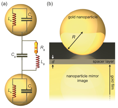
Previously we considered the ratio of the screened charge to the charge stored on a capacitor without any conductive link [24]. This simplified picture can be described by a resistor in series with the coupling capacitor effectively reducing the voltage at the capacitor. While this approach works well for describing relative changes of the charge stored on the capacitor per optical cycle it is not capable of predicting the absolute value of the resonance wavelength. Therefore we use here an equivalent parallel circuit, which is composed of a capacitor shunted with a resistor and an inductor, which reproduces the behaviour of conductive paths through the gap, in series (see Fig. 2(a)). For a sufficiently low resistance the inductor produces a screening voltage, while for high resistance the inductor plays no role and the coupling is purely dominated by the capacitor. If the gap inductance is large, then little screening is obtained because charge cannot short across the gap within an optical cycle. Hence the fully screened mode at large conductance is blue-shifted furthest if the gap inductance approaches the inductance given by the individual sphere. The resonance frequency of this circuit found when is
| (2) |
Simplifying this equation (see appendix A) yields the resonance condition:
| (3) |
where is the normalised resonance frequency, the dimer mode , normalised gap capacitance , normalised inductive coupling rate , and normalised loss rate . For the case of very low conductivity () which gives the typical coupled mode of the bonding dimer plasmon (BDP) this can be simplified to giving resonant wavelength
| (4) |
for coupled plasmonic particles. In the extreme case of high conductivity ( so ), Eq. (3) yields the screened coupled plasmon mode (SBDP)
| (5) |
which is a central result of our paper.
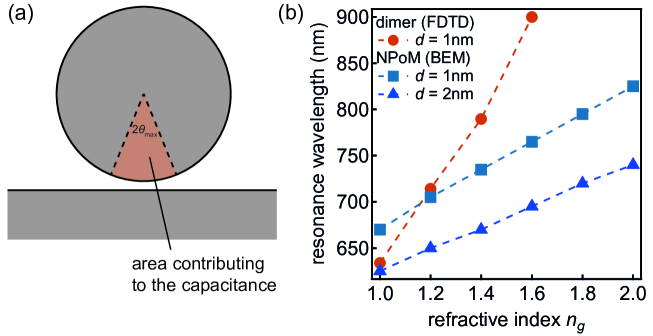
We now use the nanoparticle on mirror geometry to test this model. In this geometry a gold nanoparticle is placed on a thin spacer layer above a gold film (Fig. 2(b)). Dipoles induced in the nanoparticle can couple to their image charges forming a tightly confined coupled plasmon mode[28]. The gap capacitance for this geometry can be obtained following Hudlet et al. [29] (see appendix B):
| (6) |
with refractive index of the material in the gap , separation between nanoparticle and gold film , and parameters (which arises from the laterally localised electric field) and (which arises from the specific NPoM geometry, appendix B). To check the validity of the model simulations were performed using the full electrodynamic boundary-element method (BEM) [6, 30].
Additional experimental data are obtained by assembling spacers of self-assembled monolayers (SAMs) of aliphatic monothiols with from 3 to 17 on atomically flat template stripped gold [31]. The thickness of each SAM is measured using spectroscopic ellipsometry. Subsequently, gold nanoparticles are assembled on top of these SAMs. The resonance wavelengths in air () of more than 1,000 particles per sample were recorded using a fully automated darkfield microscope and cooled spectrometer. Further experimental details can be found in the appendix C and elsewhere [32]. The average resonance wavelengths and standard errors were determined by fitting Gaussian distributions to the histograms (see appendix C).
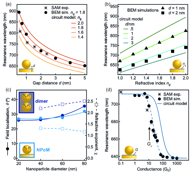
Comparing our analytical circuit model, BEM simulations, and experimental data shows excellent agreement. The characteristic continuous blueshift of the coupled plasmon resonance for increasing gap spacing and different refractive indices is clearly shown in Fig. 3(a). Similarly the expected linear redshift with increasing refractive index is completely reproduced (Fig. 3(b)).
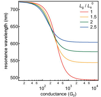
The gap capacitance parameters are found to be weakly dependent on the nanoparticle size and geometry (Fig. 3(c)). This is because the field localisation (described here by ) is slightly different between NPoM and two nanoparticles in a dimer, in particular in the effects of increasing the spacer refractive index (see appendix B). Most crucially, the model predicts for the first time analytically the blue shift of the coupled plasmon when the gap starts conducting (Fig. 3(d)). While such effects from mixed conducting SAM layers have only previously been computed in full simulations [27], our analytic solution indeed captures three important properties of such a conductive system: (i) the need to exceed a critical conductance , (ii) continuous blue shifts with increasing conductance, and (iii) the saturation of the screening for large conductances. The exact critical conductance is overestimated in our model (Fig. 3(d) solid line), and fits much better when shifted by (dashed Fig. 3(d)), however the order of magnitude is acceptable. Using Eq. (3), we obtain an analytical estimate for the critical conductance, where is the impedance of free space (see appendix A).
4 The role of the gap inductance
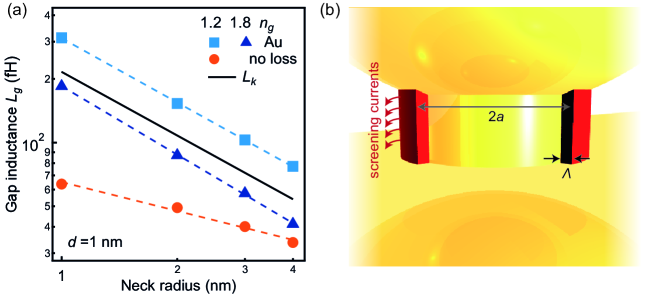
The maximum blue shift when the gap becomes conducting (saturating the screening) is set by the inductance of this filament, which screens charges in the gap expelling the electric field. To understand what sets the value of this inductance we perform BEM simulations for both insulating and completely conducting gaps. The conductive region was modelled as a cylinder connecting the gold spheres. Varying the neck radius a reveals that for gold while for an ideal conductor (with extremely low damping) we find (Fig. 4(a)). This dependence arises because is dominated by the kinetic inductance produced by the magnetic field in the gap encircling the current acting to drag back the electrons. To obtain we equate the kinetic energy of moving electrons with the energy of an inductor with velocity , current , area , and , giving with density of mobile carriers in the conducting link and electron mass [33]. The electric field however can only penetrate a certain distance into the connecting filament so that current flows only in an outer sheath (Fig. 4(b)) giving
| (7) |
with the geometry factor . We find screening depths of (appendix A) so for very narrow gold gaps, which then accounts extremely well for the dependence in the full simulations of and even produces quantitative agreement with the magnitude of the gap inductance (Fig. 4(a)). For an imperfect metal the screening depth cannot be ignored, giving a modified form which depends also on (appendix A). The blue-shift of the coupled plasmon seen when conducting links are inserted between plasmonic elements can thus be understood as arising from their kinetic inductance. Inserting Eq. (7) into Eq. (5), we find an analytic form of the blue-shift
| (8) |
which for small gaps depends linearly on the ratio of neck to nanoparticle radius. These shifts can indeed be large (we obtain spectral shifts experimentally, see Fig. 3(d)). We also note the interesting ramification that will depend on the morphology of links across a plasmonic gap. This opens great opportunities in understanding nanoscale conducting elements purely through optical spectroscopy, which can then follow dynamic processes.
5 Conclusion
In conclusion, we present a circuit model which can be used to describe coupled plasmon resonances in both capacitive and conductive coupling regimes. It provides an exceptionally straightforward way to calculate analytically the resonance wavelength for different gap sizes, nanoparticle sizes, refractive indices, and linker conductivities. We showed how a test geometry based on a nanoparticle on gold mirror gives excellent agreement of the model with both experiment and simulation. This model allows us to identify the crucial properties of the system, and resolves the key role of kinetic inductance. Further geometries can easily be incorporated by adjusting the capacitances of both the gap region and the individual plasmonic systems.
Appendix
Appendix A Derivation of the model
The resonance frequency of the circuit shown in Fig. 2(a) (main text) is found when :
| (9) |
| (10) |
Using the Drude model Eq. (1) for and replacing all frequencies by yields:
| (11) |
with , , and . Rearranging Eq. (11) yields:
| (12) |
| (13) |
| (14) |
To look for the real part of this expression we multiply with the complex conjugate of the denominator, and set the numerator to zero:
| (15) |
| (16) |
| (17) |
| (18) |
| (19) |
We find to good approximation that , simplifying Eq. (19) further. Using and yields:
| (20) |
This is Eq. (3) in the main text. The solution to this gives the spectral position of the dimer resonance, given suitable parameters.
A.1 Conductive gaps
In the case of conductive gaps, the resistance controls the crossover between the coupled resonance and the screened coupled resonance. The inductance determines the spectral position of the fully screened mode (i.e. highly conducting gap where becomes small), so that . We write this in terms of the ratio between gap and sphere inductance, , with taken at the single particle resonance. If the gap inductance is large, then little screening is obtained because charge cannot short across the gap within an optical cycle. Hence the fully screened mode at large conductance is blue-shifted furthest if the gap inductance approaches the inductance given by the individual sphere (). The cross-over conductance between the two regimes is given by which implies a critical conductance . This predicts indeed the right magnitude of the critical conductance compared to the full BEM simulations. Changing the gap inductance thus modifies both the wavelength of the screened mode, as well as the critical conductance (Fig. 5).
For the kinetic inductance as described in the main text, we can substitute into
| (21) |
using with , , and then using a binomial expansion we find:
| (22) |
which gives the result for the blue shift in the main text.
A.2 Screening depths
In the small-gap metal-insulator-metal structures here, we find the propagation wavevector in a gap of width
| (23) |
which gives the field in the metal
| (24) |
Solving for the penetration depth of optical field inside the metal
| (25) |
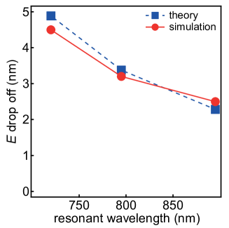
We compare below this penetration depth (Fig. 6 blue squares) with full BEM simulations of the exact NPoM structures (spherical 80nm Au NP) from which we also extract the field penetration (Fig. 6 red circles). This gives a very good match for the various ( [nm],) = (1,1.3), (1,1.8), (0.5,1.8) which shift the resonant mode wavelength across the near infrared.
We can also substitute in the Drude model, and providing the damping is not too large we find
| (26) |
Appendix B Nanoparticle on mirror capacitance model
Modelling the gap capacitance is key to obtain reliable values for the resonance frequency and for obtaining the correct dependencies on distance and refractive index. The simplest approximation is a plate capacitor, with area , filled with a material with refractive index :
| (27) |
A more precise description of the capacitance of a spherical nanoparticle on a metallic mirror is[29]:
| (28) |
By considering that the gap occupies only a small area of the full sphere (i.e. restricting the upper integration boundary to a small angle ) and using small angle approximations yields (see illustration in Fig. 7(a)):
| (29) |
By comparing the refractive index dependency obtained from electromagnetic simulations (finite-difference time-domain - FDTD & boundary element method - BEM) we find that depending on the exact geometry the exponent of the refractive index deviates from two. We have performed simulations for different geometries and different refractive indices. Plotting (calculated from the resonance wavelength using Eq. (4)) vs allows to extract the refractive index exponent . Fig. 8 shows for both nanoparticle dimers and the nanoparticle on mirror geometry.
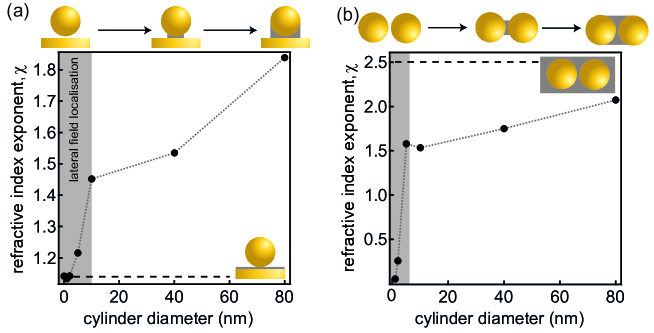
Fig. 8 shows that using a cylindrical material in the gap can strongly influence the refractive index dependency; we observe two regions: For cylinder diameters smaller than the lateral field localization a steep increase is observed indicating that both the single particle mode and the coupled mode shift their spectral position. A second region is observed for diameter larger than the plasmon dimension, here the dependence is shallow as mostly the single particle mode is changed. For an extended film covering the whole gold substrate we find , for dimers submerged in a medium with a certain refractive .
Appendix C Experimental details & results
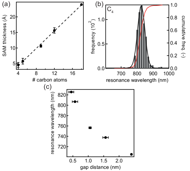
As described in the main text self-assembled monolayers of different length aliphatic thiols were used as experimental spacer. For each SAM the thickness of three samples (three spots per sample) were measured by phase modulated ellipsometry. Fig. 9(a) shows the determined SAM thickness as a function of the number of carbon atoms. For each SAM a sample was covered with 80 nm gold nanoparticles. The resonance wavelength of over 1,000 nanoparticles was measured per sample using an automated Olympus BX51 darkfield microscope. Further details on the spectroscopy and evaluation can be found elsewhere [32]. Fig. 9(b) shows exemplarily an obtained resonance wavelength distribution for butanethiol (C4) self-assembled monolayer as a spacer layer. The resonance wavelengths for all samples as a function of the SAM thickness can be found in Fig. 9(c).
C.1 Sample Preparation
A 100 nm thick gold film was evaporated on a silicon (100) wafer (Kurt J. Lesker Company, PVD 200) using an evaporation rate of 1 Å/s with a base pressure of mbar. To obtain atomically smooth gold surfaces a standard template stripping method was applied: small silicon (100) pieces were glued to the evaporated gold surface using Epo-Tek 377 epoxy glue. After curing the glue the sample can be pealed of the silicon wafer revealing a fresh, clean surface with excellent surface roughness [31]. 1-butanethiol (C4), 1-pentanethiol (C5), 1-nonanethiol (C9), 1-dodecanethiol (C12), and 1-octadecanethiol (C18) (Sigma-Aldrich, ) self-assembled monolayers were assembled on these freshly prepared surfaces by immersing in 1 mM solution for 22 h. Subsequently, the samples were thoroughly rinsed with ethanol, briefly cleaned in an ultrasonic bath to remove excess unbound thiols, and blown dry. The samples were stored under a constant nitrogen flow until they were used. 80 nm gold nanoparticles were used as received from BBI Solutions. To deposit the nanoparticles on the SAM the previously prepared samples were immersed in the nanoparticle solution. The time was adjusted in order to reach a uniform but sparse coverage that allows spectroscopic investigations of individual nanoparticles. Excess nanoparticles were rinsed off with distilled water and the samples were dried with nitrogen.
C.2 Experimental
Darkfield spectra of over 1,000 nanoparticles were recorded using a fully automated Olympus BX51 microscope in a reflective dark field geometry. The scattered light was collected with a 100 long working distance objective (NA 0.8) and analysed with a TEC-cooled Ocean Optics QE65000 spectrometer. Further details can be found elsewhere [32].
C.3 Ellipsometry
The thickness of the self-assembled monolayers was measured using a Jobin-Yvon UVISEL spectroscopic ellipsometer at angle of incidence 70∘ and wavelengths from 300-800 nm. The base layer permittivity is obtained from a clean gold substrate and the dielectric properties of the SAMs described using a Cauchy model with refractive index of 1.45 (as determined by [34, 35]).
Acknowledgments
We acknowledge financial support from EPSRC grant EP/G060649/1, EP/I012060/1, EP/L027151/1, EP/K028510/1, ERC grant LINASS 320503. FB acknowledges support from the Winton Programme for the Physics of Sustainability. RC wishes to acknowledge financial support from St. John’s College, Cambridge for Dr. Manmohan Singh Scholarship. CT and JA acknowledge financial support from Project FIS2013- 41184-P from MINECO, ETORTEK 2014-15 of the Basque Department of Industry and IT756-13 from the Basque consolidated groups.