Signatures of single quantum dots in graphene nanoribbons within the quantum Hall regime
Abstract
We report on the observation of periodic conductance oscillations near quantum Hall plateaus in suspended graphene nanoribbons. They are attributed to single quantum dots that form in the narrowest part of the ribbon, in the valleys and hills of a disorder potential. In a wide flake with two gates, a double-dot system’s signature has been observed. Electrostatic confinement is enabled in single-layer graphene due to the gaps that form between Landau levels, suggesting a way to create gate-defined quantum dots that can be accessed with quantum Hall edge states.
pacs:
73.23.-b, 73.63.Nm, 74.45.+c, 03.67.BgIntroduction— The Dirac spectrum results in several peculiar features in the charge transport of graphene, such as Klein tunneling, or the special Berry phase and the half-integer quantum Hall-effect Katsnelson et al. (2006); Novoselov et al. (2005); Zhang et al. (2005); Neto et al. (2009). The high mobility of graphene offers a good platform for field effect transistors, whereas the low spin-orbit coupling Gmitra et al. (2009) and small amount of nuclear spins make it promising for the realization of long-lifetime spin qubits DiVincenzo and Loss (1998); Loss and DiVincenzo (1998); Trauzettel et al. (2007); Droth and Burkard (2015). However, from an application point of view, the absence of a band gap places limitations: it hinders effective electrostatic confinement of electrons, which makes the fabrication of spin qubits challenging and results in high OFF state currents for field effect transistors.
Creating nanoribbons in graphene provides a way to generate a band gap due to one dimensional confinement Son et al. (2006a, b). The common technique to confine electrons in a graphene quantum dot (QD) or ribbon is based on tailoring the graphene sheet by etching. In QD devices Stampfer et al. (2008); Liu et al. (2009); Moriyama et al. (2009); Schnez et al. (2010) thin graphene nanoribbon sections play the role of tunnel barriers. Promising results have been achieved, e.g. detection of the QD’s orbital spectrum Ponomarenko et al. (2008); Liu et al. (2010), or observation of the spin-filling sequence Güttinger et al. (2010). However, edge roughness, inhomogeneities in the substrate, fabrication residues, and the unpredictability of the nanoribbons that act as tunnel barriers place clear limitations to this technology Han et al. (2007); Stampfer et al. (2009); Han et al. (2010); Gallagher et al. (2010).
Other confinement strategies involve opening a gap in bilayer graphene using perpendicular electric fields, or exploiting the angle-dependent transmission in p-n junctions. Both techniques require ultra-clean high mobility junctions, for which encapsulation in hBN Dean et al. (2010); Mayorov et al. (2011) or suspension of the graphene flake Bolotin et al. (2008); Tombros et al. (2011) is required. Recently quantum dots and point contacts have been created by utilizing the gap opening in bilayer graphene Allen et al. (2012); Goossens et al. (2012); Varlet et al. (2014). Futhermore, beamsplitters and waveguides were fabricated using p-n junctions Rickhaus et al. (2015a, b), however, the confinement offered by the p-n transition is soft and electrons can leak out.
In this paper we focus on a different method, which uses magnetic fields to form a gap in the bulk of single-layer graphene. Applying a perpendicular magnetic field , Landau levels (LLs) form with remarkably high energy spacing: for example, the energy of the fourfold degenerate, LL is . Combining this field-induced gap with a local electrostatic field, a confinement potential for quantum dots can be achieved, which can be read out via edge states. In this work we present the transport characterization of suspended single-layer graphene strips where single and double dots form based on this principle.
Measurements on a clean ribbon— We have fabricated suspended graphene nanoribbons, an approximate geometry of which is shown in Fig. 1a. We have used a polymer-based suspension method following Refs. 26; 32 and a transfer method by Ref. 23. Details are given in the Methods section. Measurements were done at 1.5 K using low frequency lock-in technique.
Fig. 1b shows the two-terminal differential conductance of a nanoribbon (designated R1) as a function of the magnetic field and the electron density , tuned by the gate voltage . A conductance plateau takes shape at filling factor, slightly below due to a contact resistance of . Above 3 T, a widening zero-conductance region appears around the Dirac-point, caused by the splitting of the fourfold degenerate 0th Landau level due to finite-range Coulomb-interactions Zhang et al. (2006); Young et al. (2012); Yu et al. (2013); Abanin et al. (2013); Roy et al. (2014). As confirmed by bias measurements, a true gap - in the order of 10 meV in this -field range Roy et al. (2014) - forms between the upper and lower split 0th LL (denoted by indices and ), schematically shown in Fig. 1c.
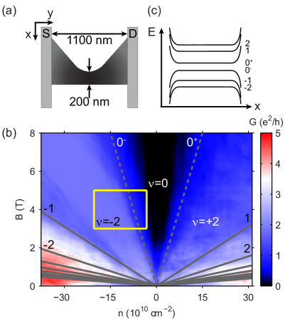
A zoom of the yellow rectangle in Fig. 1b can be seen in Fig. 2a, showing parts of the plateaus at and . The -2 plateau is separated from the gap by a wide transition region, where the th LL is gradually filled, allowing scattering between edge states and contacts. A cut at 5 T (Fig. 2b) shows that the random conductance fluctutations visible in the transition region become very regular close to the gap or the plateau. Zooms of these regions are shown in the insets of the same figure. These fluctuations are periodic in nature: at the plateau-edge, 18 oscillations can be seen with a period of 0.17 V, and at the gap-edge there are about 30 oscillations with 0.09 V spacing. We call the regular oscillations on the edge of the plateau ”plateau-edge oscillations”, and the ones close to the region ”gap-edge oscillations”. Similar features were observed in the conductance band.
The plateau-edge and gap-edge oscillations are most visible between the red and blue dashed lines in Fig. 2a, and are parallel with the -2 and the 0 filling factor directions, respectively. These directions are marked with short red and blue lines at the top of the figure. Fig. 2c shows the oscillations’ average periodicity as a function of magnetic field: red dots correspond to plateau-edge, while blue circles correspond to gap-edge oscillations. Their periodicity is approximately constant for a wide range of magnetic fields, except for the gap-edge oscillations’ below 4 T, where the fluctuations become irregular. In the following, the mechanisms behind both random and regular conductance fluctuations, and their behavior, are addressed.
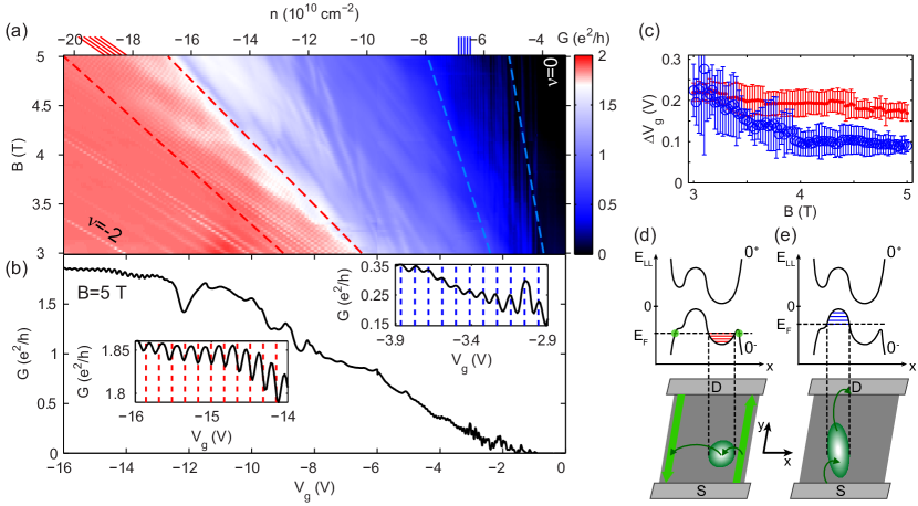
The transition region between the -2 and 0 plateaus points to a disorder potential that widens the th LL in energy. In this region, the LL is partially filled, and the bulk is conducting due to delocalized states that connect edge states and contacts. Whereas near small, or almost complete filling, these states are localized to extrema of the potential landscape, stabilizing the quantum Hall plateaus. When a LL is almost empty, only the lowest disorder-potential valleys are filled with electrons, while in an almost full LL, the same happens in the hole picture. An example of the potential is shown in the top halves of Figs. 2d, e. The conductance fluctuations observed near low and high filling may be resonant tunnelling events via the eigenenergy levels of the localized states. However, random potential features would produce eigenspectra that give random curves on the - map Ilani et al. (2004); Martin et al. (2009), contrary to the parallel, regular lines of the plateau and gap edges.
The fluctuation lines’ behavior is explained if we take electrostatic interactions into account. The disorder potential will be partially screened due to the electrons or holes present in the LL, which will accumulate in potential valleys and hills. Full screening, however, is not possible due to the limited number of states allowed within a given LL. The filled potential features result in a series of electron or hole islands with electrostatic charging energy, i.e. quantum dots, separated by tunnel barriers (Figs. 2d, e), not unlike the finite -field case of Ref. 27. Disorder-induced localized states have been visualized in 2DEGs and graphene using local probe techniques, such as single electron transistor Ilani et al. (2004); Martin et al. (2009), scanning tunnelling microscopy and spectroscopy Miller et al. (2010); Jung et al. (2011) and spacially resolved photocurrent measurements Nazin et al. (2010). Since these quantum dots cause scattering events between quantum Hall edge states and contacts (see the bottom halves of Figs. 2d, e), their signature can be observed in conductance (Refs. 43; 44; 45, and even Refs. 46; 47; 48) and transconductance measurements Lee et al. (2012).
The magnetic field dependence of the fluctuations, i.e. gathering together into sets of lines parallel with filling factor directions, is easily explained. Along a fluctuation line on the map, the average electron (hole) number on the originating dot is constant. Accordingly, the electron (hole) density belonging to the current LL is also constant, thus the fluctuations are parallel with the conductance plateau which corresponds to the empty (full) LL.
For multiple dots, a random series of parallel lines is expected close to the plateau and gap edge, contrary to the periodic oscillations seen in the experiment in Fig. 2. Therefore, a single electron and hole QD must dominate scattering events for low and high filling of the th LL, respectively. The questions arise, what makes a dot dominant, and in what circumstances? In the following, we give a physical picture and highlight the different mechanisms behind the plateau-edge and gap-edge oscillations.
Since the plateau-edge oscillations have a negative contribution to the conductance plateau (see left inset of Fig. 2b), we infer that the dominant electron quantum dot connects mainly the edge states, causing backscattering. For a schematic drawing of the process, see Fig. 2d. In contrast, when we approach the gap, the th LL is almost filled with electrons, and a single hole QD’s charging dominates. In this case, however, no edge states exist, therefore the gap-edge oscillations can only result from forward scattering between the contacts (schematic in Fig. 2e). We attribute the dominant quantum dots to local potential extrema situated near the narrowest part of the ribbon, since conductance is most sensitive to this section. If the dominant dot were elsewhere, the observed oscillations would likely be irregular due to the contribution of other dots to either scattering mechanism. Nonetheless, for the hole QD, the rest of the dot network - in the wider sections of the sample - is essential to establish a connection toward the contacts.
The estimation of the electron and hole dots’ sizes supports this suggestion. The exact capacitance per area can be calculated from the slope of the -2 plateau center, since the filling factor relates to the density via . We calculate the capacitance per area, , to be , which agrees well with electrostatic calculations on similar devices Rickhaus et al. (2015c); Liu et al. (2015). Using the average gate voltage periodicities in Fig. 2c, we estimate that the electron quantum dot responsible for the plateau-edge oscillations extends over an area of approximately nm2, while the hole quantum dot - causing the gap-edge oscillations - is nm2 in size. Since the ribbon’s narrowest part is nm wide, quantum dots with the above areas are able to cause scattering events across the width or length of the constriction, thus connecting the edge states or the wider, highly doped regions (and therefore the contacts).
Since the dominant QDs are formed in potential extrema of the constriction, their signatures are best seen at either low or high Landau level filling, between the dashed lines in Fig. 2a. Moving the Fermi level toward the LL’s center, more potential valleys or hills start to play a role in transport, and the fluctuation pattern becomes random. Eventually, all charges become delocalized, and the bulk becomes conducting. In contrast, increasing the magnetic field while following a fluctuation line from its high-visibility region between the red (blue) dashed lines of Fig. 2a, and into the -2 (0) plateau, the size and coupling of localized and edge states decreases. Tunnelling rates are suppressed, and eventually only the flat plateau remains visible.
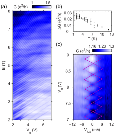
Coulomb peak behavior— We reproduced the oscillation pattern in the conductance band of a second nanoribbon, designated R2, that didn’t show well-developed quantum Hall plateaus. Its two-terminal conductance, displayed in Fig. 3a, shows regularly placed conductance dips, their lines parallel with the expected slope of the plateau. Therefore, they are attributed to a hole dot belonging to the electron side of the 0th LL, causing backscattering. Fig. 3b shows their peak-to-peak amplitude at 8 T as a function of temperature. The fluctuations disappear in the range, where the charging energy of the QD becomes comparable with thermal broadening. Since the oscillations’ width is similar to their period, fitting curves on the series of inverted Coulomb-peaks, or their amplitude - to analyze height and width change with temperature - can’t be done without a huge margin of error.
The fluctuations’ slope, parallel with the direction, gives the gate capacitance per area, which is , or . With the oscillation period, we estimate the area of the dot to be approximately nm2. In Fig. 3c the dominant quantum dot’s stability diagram, i.e. conductance versus and (source-drain voltage), is shown. The conductance contribution of the Coulomb-diamonds is negative, since the dot causes backscattering. Their size gives a charging energy of , allowing us to calculate the self capacitance: . As a comparison, the gate capacitance is . By counting the number of regular oscillations, we estimate that the height of the potential hill that defines the hole QD is a remarkable 260 meV, comparable to the energy of the first LL at 8 T, meV. However, the charging energy deduced from the size of the Coulomb diamonds in the source-drain axes might be overestimated, since not all of the bias voltage drops at the barriers defining the quantum dot.
Double-dot system in a wide sample— To examine the role of sample width, we measured the conductance of a 1.8 m wide and 0.8 m long graphene strip. The density of the device could be locally tuned by two bottom gates, g1 and g2, that were aligned in parallel with the sample current direction, as shown in the schematic in Fig. 4a.
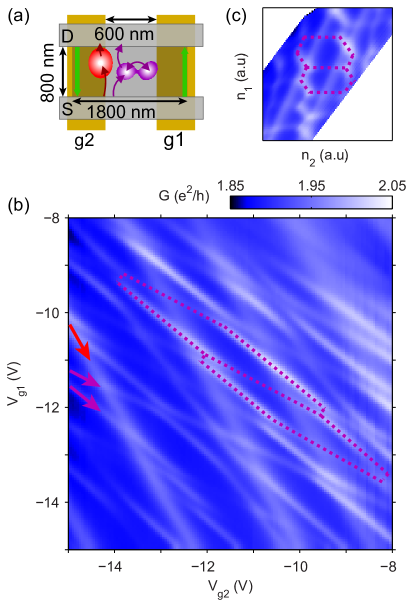
Fig. 4b shows the conductance of the quantum Hall plateau near filling of both sides, as a function of the two gate voltages, at 4 T. A random structure of lines with different slopes - some of them highlighted by arrows - are conspicuous on the conductance map, indicating that QDs are tuned by both voltages. The slope of a dot’s fluctuation lines is determined by the dot’s position relative to the two gate electrodes. As expected, the map shows the signatures of a network of QDs. Due to the low aspect ratio, scattering between contacts is much more likely than between edge states, explaining the positive conductance contribution of the dots.
Some of the fluctuation lines show avoided crossings. They have similar slopes, indicating they belong to quantum dots that are close to each other, enabling them to hybridize (purple QDs in Fig. 4a). Thus, the lines with avoided crossings belong to one or more double-dot systems. The expected hexagonal pattern of a double dot is highlighted in purple as a guide to the eye, and is even more evident in Fig. 4c, where the map is distorted to compensate for cross-capacitances. This way the conductance is shown as a function of the individual dot charges of this double-dot system. One set of lines is stronger, suggesting one dot is better coupled to the contact electrodes than the other.
Summary and outlook— A band gap is essential to create graphene transistors and spin qubits. However, Klein tunnelling limits the effectiveness of electrostatic confinement, while hard wall confinement (etching) introduces further obstacles. In the quantum Hall regime, a disorder potential can act as confinement due to the bulk gaps between Landau levels. As a result, a network of quantum dots form. In our nanoribbons the small sample width enabled a single QD to dominate that could be read out not only by contacts, but also by edge channels. In a wide flake with two gates a double-dot system’s hexagonal pattern was observed. This mechanism suggests a way to electrostatically confine electrons in clean single-layer graphene devices using multiple gate electrodes. With suitable geometries, the creation of quantized conducting channels, single and double quantum dots, quantum point contacts, and even interferometers becomes possible.
Acknowledgements— We acknowledge useful discussions with Romain Maurand, Andreas Baumgartner, András Pályi, Péter Rakyta, László Oroszlány, Matthias Droth, and Csaba Tőke. This work was funded by the EU ERC CooPairEnt 258789, Hungarian Grants No. OTKA K112918, and also the Swiss National Science Foundation, the Swiss Nanoscience Institute, the Swiss NCCR QSIT, the ERC Advanced Investigator Grant QUEST and the EU Graphene Flagship project. S.C. was supported by the Bolyai Scholarship.
Methods— Fabrication steps followed Refs. 26; 32. First, 5/55 nm thick Pd/Al or Ti/Au bottom gates were fabricated on a p:Si/SiO2 layer, which were covered first with a 50 nm ALD-grown insulating layer, second with 600 nm thick LOR resist. Graphene was exfoliated onto a separate wafer and transferred using the method described in Ref. 23. Subsequently, the flake was contacted with 40 nm thick Pd wires, and etched using e-beam lithography and reactive ion etching. Approximate dimensions of ribbons R1, R2 are given in Fig. 1a. Finally, graphene was suspended by exposing and developing the LOR resist below. Samples were current annealed at low temperature to remove solvent and polymer residues. Measurements were carried out at 1.5 K, using standard lock-in technique. The Dirac-points of the ribbons R1, R2, and the wide sample were at approximately , 0, and 1 V, respectively.
References
- Katsnelson et al. (2006) M. Katsnelson, K. Novoselov, and A. Geim, Nature Physics 2, 620 (2006).
- Novoselov et al. (2005) K. Novoselov, A. K. Geim, S. Morozov, D. Jiang, M. Katsnelson, I. Grigorieva, S. Dubonos, and A. Firsov, Nature 438, 197 (2005).
- Zhang et al. (2005) Y. Zhang, Y.-W. Tan, H. L. Stormer, and P. Kim, Nature 438, 201 (2005).
- Neto et al. (2009) A. C. Neto, F. Guinea, N. Peres, K. S. Novoselov, and A. K. Geim, Reviews of modern physics 81, 109 (2009).
- Gmitra et al. (2009) M. Gmitra, S. Konschuh, C. Ertler, C. Ambrosch-Draxl, and J. Fabian, Physical Review B 80, 235431 (2009).
- DiVincenzo and Loss (1998) D. P. DiVincenzo and D. Loss, Superlattices and Microstructures 23, 419 (1998).
- Loss and DiVincenzo (1998) D. Loss and D. P. DiVincenzo, Physical Review A 57, 120 (1998).
- Trauzettel et al. (2007) B. Trauzettel, D. V. Bulaev, D. Loss, and G. Burkard, Nature Physics 3, 192 (2007).
- Droth and Burkard (2015) M. Droth and G. Burkard, Physica Status Solidi (RRL)-Rapid Research Letters 9999, 1 (2015).
- Son et al. (2006a) Y.-W. Son, M. L. Cohen, and S. G. Louie, Physical Review Letters 97, 216803 (2006a).
- Son et al. (2006b) Y.-W. Son, M. L. Cohen, and S. G. Louie, Nature 444, 347 (2006b).
- Stampfer et al. (2008) C. Stampfer, E. Schurtenberger, F. Molitor, J. Guttinger, T. Ihn, and K. Ensslin, Nano Letters 8, 2378 (2008).
- Liu et al. (2009) X. Liu, J. B. Oostinga, A. F. Morpurgo, and L. M. Vandersypen, Physical Review B 80, 121407 (2009).
- Moriyama et al. (2009) S. Moriyama, D. Tsuya, E. Watanabe, S. Uji, M. Shimizu, T. Mori, T. Yamaguchi, and K. Ishibashi, Nano Letters 9, 2891 (2009).
- Schnez et al. (2010) S. Schnez, J. Güttinger, M. Huefner, C. Stampfer, K. Ensslin, and T. Ihn, Physical Review B 82, 165445 (2010).
- Ponomarenko et al. (2008) L. Ponomarenko, F. Schedin, M. Katsnelson, R. Yang, E. Hill, K. Novoselov, and A. Geim, Science 320, 356 (2008).
- Liu et al. (2010) X. L. Liu, D. Hug, and L. M. Vandersypen, Nano Letters 10, 1623 (2010).
- Güttinger et al. (2010) J. Güttinger, T. Frey, C. Stampfer, T. Ihn, and K. Ensslin, Physical Review Letters 105, 116801 (2010).
- Han et al. (2007) M. Y. Han, B. Özyilmaz, Y. Zhang, and P. Kim, Physical Review Letters 98, 206805 (2007).
- Stampfer et al. (2009) C. Stampfer, J. Güttinger, S. Hellmüller, F. Molitor, K. Ensslin, and T. Ihn, Physical Review Letters 102, 056403 (2009).
- Han et al. (2010) M. Y. Han, J. C. Brant, and P. Kim, Physical Review Letters 104, 056801 (2010).
- Gallagher et al. (2010) P. Gallagher, K. Todd, and D. Goldhaber-Gordon, Physical Review B 81, 115409 (2010).
- Dean et al. (2010) C. Dean, A. Young, I. Meric, C. Lee, L. Wang, S. Sorgenfrei, K. Watanabe, T. Taniguchi, P. Kim, K. Shepard, et al., Nature Nanotechnology 5, 722 (2010).
- Mayorov et al. (2011) A. S. Mayorov, R. V. Gorbachev, S. V. Morozov, L. Britnell, R. Jalil, L. A. Ponomarenko, P. Blake, K. S. Novoselov, K. Watanabe, T. Taniguchi, et al., Nano Letters 11, 2396 (2011).
- Bolotin et al. (2008) K. I. Bolotin, K. Sikes, Z. Jiang, M. Klima, G. Fudenberg, J. Hone, P. Kim, and H. Stormer, Solid State Communications 146, 351 (2008).
- Tombros et al. (2011) N. Tombros, A. Veligura, J. Junesch, J. J. van den Berg, P. J. Zomer, M. Wojtaszek, I. J. V. Marun, H. T. Jonkman, and B. J. van Wees, Journal of Applied Physics 109, 093702 (2011).
- Allen et al. (2012) M. T. Allen, J. Martin, and A. Yacoby, Nature Communications 3, 934 (2012).
- Goossens et al. (2012) A. S. M. Goossens, S. C. Driessen, T. A. Baart, K. Watanabe, T. Taniguchi, and L. M. Vandersypen, Nano Letters 12, 4656 (2012).
- Varlet et al. (2014) A. Varlet, M.-H. Liu, V. Krueckl, D. Bischoff, P. Simonet, K. Watanabe, T. Taniguchi, K. Richter, K. Ensslin, T. Ihn, et al., Physical Review Letters 113, 116601 (2014).
- Rickhaus et al. (2015a) P. Rickhaus, M.-H. Liu, P. Makk, R. Maurand, S. Hess, S. Zihlmann, M. Weiss, K. Richter, and C. Schönenberger, Nano Letters 15, 5819 (2015a).
- Rickhaus et al. (2015b) P. Rickhaus, P. Makk, M.-H. Liu, K. Richter, and C. Schönenberger, Applied Physics Letters 107, 251901 (2015b).
- Maurand et al. (2014) R. Maurand, P. Rickhaus, P. Makk, S. Hess, E. Tovari, C. Handschin, M. Weiss, and C. Schönenberger, Carbon 79, 486 (2014).
- Zhang et al. (2006) Y. Zhang, Z. Jiang, J. Small, M. Purewal, Y.-W. Tan, M. Fazlollahi, J. Chudow, J. Jaszczak, H. Stormer, and P. Kim, Physical Review Letters 96, 136806 (2006).
- Young et al. (2012) A. F. Young, C. R. Dean, L. Wang, H. Ren, P. Cadden-Zimansky, K. Watanabe, T. Taniguchi, J. Hone, K. L. Shepard, and P. Kim, Nature Physics 8, 550 (2012).
- Yu et al. (2013) G. Yu, R. Jalil, B. Belle, A. S. Mayorov, P. Blake, F. Schedin, S. V. Morozov, L. A. Ponomarenko, F. Chiappini, S. Wiedmann, et al., Proceedings of the National Academy of Sciences 110, 3282 (2013).
- Abanin et al. (2013) D. A. Abanin, B. E. Feldman, A. Yacoby, and B. I. Halperin, Physical Review B 88, 115407 (2013).
- Roy et al. (2014) B. Roy, M. P. Kennett, and S. D. Sarma, Physical Review B 90, 201409 (2014).
- Ilani et al. (2004) S. Ilani, J. Martin, E. Teitelbaum, J. Smet, D. Mahalu, V. Umansky, and A. Yacoby, Nature 427, 328 (2004).
- Martin et al. (2009) J. Martin, N. Akerman, G. Ulbricht, T. Lohmann, K. Von Klitzing, J. Smet, and A. Yacoby, Nature Physics 5, 669 (2009).
- Miller et al. (2010) D. L. Miller, K. D. Kubista, G. M. Rutter, M. Ruan, W. A. de Heer, M. Kindermann, P. N. First, and J. A. Stroscio, Nature Physics 6, 811 (2010).
- Jung et al. (2011) S. Jung, G. M. Rutter, N. N. Klimov, D. B. Newell, I. Calizo, A. R. Hight-Walker, N. B. Zhitenev, and J. A. Stroscio, Nature Physics 7, 245 (2011).
- Nazin et al. (2010) G. Nazin, Y. Zhang, L. Zhang, E. Sutter, and P. Sutter, Nature Physics 6, 870 (2010).
- Cobden et al. (1999) D. H. Cobden, C. Barnes, and C. Ford, Physical Review Letters 82, 4695 (1999).
- Velasco Jr et al. (2010) J. Velasco Jr, G. Liu, L. Jing, P. Kratz, H. Zhang, W. Bao, M. Bockrath, C. N. Lau, et al., Physical Review B 81, 121407 (2010).
- Branchaud et al. (2010) S. Branchaud, A. Kam, P. Zawadzki, F. M. Peeters, and A. S. Sachrajda, Physical Review B 81, 121406 (2010).
- Zhang et al. (2009) Y. Zhang, D. T. McClure, E. M. Levenson-Falk, C. M. Marcus, L. N. Pfeiffer, and K. W. West, Physical Review B 79, 241304 (2009).
- McClure et al. (2009) D. T. McClure, Y. Zhang, B. Rosenow, E. M. Levenson-Falk, C. M. Marcus, L. Pfeiffer, and K. W. West, Physical Review Letters 103, 206806 (2009).
- Halperin et al. (2011) B. I. Halperin, A. Stern, I. Neder, and B. Rosenow, Physical Review B 83, 155440 (2011).
- Lee et al. (2012) D. S. Lee, V. Skákalová, R. T. Weitz, K. von Klitzing, and J. H. Smet, Physical Review Letters 109, 056602 (2012).
- Rickhaus et al. (2015c) P. Rickhaus, P. Makk, M.-H. Liu, E. Tóvári, M. Weiss, R. Maurand, K. Richter, and C. Schönenberger, Nature Communications 6, 6470 (2015c).
- Liu et al. (2015) M.-H. Liu, P. Rickhaus, P. Makk, E. Tóvári, R. Maurand, F. Tkatschenko, M. Weiss, C. Schönenberger, K. Richter, et al., Physical review letters 114, 036601 (2015).