Asymmetry-induced resistive switching in Ag-Ag2S-Ag memristors enabling a simplified atomic-scale memory design
Abstract
Prevailing models of resistive switching arising from electrochemical formation of conducting filaments across solid state ionic conductors commonly attribute the observed polarity of the voltage-biased switching to the sequence of the active and inert electrodes confining the resistive switching memory cell. Here we demonstrate equivalent, stable switching behavior in metallic Ag-Ag2S-Ag nanojunctions at room temperature. Our experimental results and numerical simulations reveal that the polarity of the switchings is solely determined by the geometrical asymmetry of the electrode surfaces. By the lithographical design of a proof of principle device we demonstrate the merits of simplified fabrication of atomic-scale, robust planar Ag2S memory cells.
pacs:
73.63.Rt, 73.61.-r, 73.40.SxAs ongoing miniaturization reaches the fundamental limitations of silicon-based complementary metal-oxide-semiconductor (CMOS) technology, the demand for alternative material platforms delivering faster, smaller, yet highly integrable logical and memory units is increasing. Self-assembled nanostructures exhibiting tunable electrical properties are primary candidates. Conducting nanofilaments formed or destroyed by reversible solid state electrochemical reactions in ionic conducting media situated between metallic electrodes have demonstrated reproducible logical and non-volatile resistance switching random access memory (ReRAM) operations Yang et al. (2013); Borghetti et al. (2010); Pershin and Di Ventra (2011a); Terabe et al. (2005); Strukov et al. (2008); Waser and Aono (2007); Terabe et al. (2007); Wang et al. (2007); Jo and Lu (2008); Aono and Hasegawa (2010); Chung et al. (2010); Linn et al. (2010); Pershin and Di Ventra (2011b); Valov et al. (2011); Torrezan et al. (2011); Hasegawa et al. (2012). The resistance of such a two-terminal memristor Chua (1971), is altered above a threshold bias () of a few hundred mV. Nonvolatile readout is performed at Gubicza et al. (2015a).
Nanofilament formation in solid state electrolytes Terabe et al. (2005, 2007); Chang et al. (2011); Ohno et al. (2011); Wagenaar et al. (2012); Strukov and Williams (2008); Xu et al. (2010); Nayak et al. (2010); Morales-Masis et al. (2009, 2010, 2011); Nayak et al. (2011); Menzel et al. (2012); Valov et al. (2012); Yang et al. (2012); Hasegawa et al. (2012); Liu et al. (2012); Menzel et al. (2013); Yang and Lu (2013); Cheng and Hu (2015) are commonly attributed to oxidation, electric-field-driven ionic migration and reduction, involving a positively charged active electrode supplying the mobile ions and a negatively charged inert electrode, where reduction can take place initializing the filament growth. At opposite polarity, the filament is dissolved. While offering extremely large switching ratios, devices operated in this regime can only perform at reduced switching speeds due to their fundamental RC limitations. Once such a conducting channel is complete, smaller but orders of magnitude faster resistance changes can be observed in the metallic regime Nardi et al. (2012); Larentis et al. (2012); Mickel et al. (2014); Torrezan et al. (2011); Geresdi et al. (2014); Gubicza et al. (2015a, b), which is also in the focus of our present study.
The central question of our paper concerns the role of the inert electrode and consequently, the polarity of the set/reset transitions. Depending on the ionic mobility and redox rates, nucleation and subsequent filament formation have been observed either at the inert or at the active electrode surfaces by in-situ methods Xu et al. (2010); Liu et al. (2012); Yang et al. (2012, 2014). After an initial nucleation phase further reduction takes place directly along the growing filament consisting of the elemental metal of the active electrode. Thus, we anticipate that resistive switching must also occur when both electrodes are fabricated from the active material. We propose that the polarity of the resistive switching is determined by the local inhomogeneity of the electric field, the latter reflecting the geometrical asymmetry of the electrode surfaces with particular emphasis on the narrowest region of the filament.
Single-component metallic junctions utilizing silver Geresdi et al. (2011a) and aluminium Schirm et al. (2013) break junctions exhibit reproducible resistive switching at cryogenic temperatures, both relying on atomic rearrangements due to electromigration. Similar experiments were also carried out using nanofabricated gold nanowires Johnson et al. (2010) at room temperature. While the operation speed of these devices were (instrumentally) limited to 100 kHz, Ag-Ag2S-PtIr memristive nanojunctions were successfully demonstrated to exhibit nanosecond switching times Geresdi et al. (2014). However, the fabrication of such ultrafast, Ag2S based memory cells would be considerably simplified if a single metallic component could be utilized for both terminals of the devices. Here we demonstrate stable resistive switchings in metallic Ag-Ag2S-Ag nanojunctions created by an STM and alternatively, in a mechanically controllable break junction (MCBJ) Muller et al. (1992) setup. The observed set/reset transitions exhibit a uniform polarity with respect to the initial asymmetry of the junction geometry in agreement with our molecular dynamical simulations. The latter reveal the kinetics of filament growth and shrinkage under various boundary conditions by taking into account electric-field-driven activated ionic migration in the Ag2S matrix. Based on these findings a proof of concept all-Ag on-chip device fabricated by standard electron beam lithography is testified to reliable memory operations.
The first set of experiments utilized an 80 nm thick Ag layer deposited onto a Si substrate followed by a 5 minutes long sulfurisation performed at 60∘C resulting in a 30 nm thick stoichiometric Ag2S cap layer on the planar Ag electrode Geresdi et al. (2011b). Nanometer-scale junctions were created between the Ag2S surface and a mechanically sharpened 99.99% pure Ag wire of 0.35 mm in diameter in STM geometry. Alternatively, Ag-Ag2S-Ag point contacts were also established by the controlled rupture of a 99.99% pure Ag wire with a diameter of 0.125 mm in the vacuum chamber of an MCBJ setup followed by a 20 minutes long in-situ sulfurisation carried out at 25∘C. During the acquisition of the current-voltage (I-V) characteristics the low frequency triangular voltage output of a data acquisition card was acting on the memristive junction and on a variable series resistor as shown in Fig. 1(b). The device’s current was monitored by a current amplifier while the voltage drop on the junction was determined numerically as . All measurements were performed at room temperature.
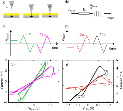
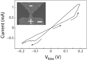
Representative I-V traces obtained in the inherently asymmetric STM geometry are displayed in Fig. 1. In order to investigate the influence of the initial electroforming process on the direction of the observed resistive switching, measurements were performed on nanojunctions established with Ag tips, which were either negatively or positively charged during approaching the Ag2S thin films, as illustrated in Fig 1(a). After forming a metallic contact, a triangular voltage signal of the same initial polarity was applied to record the I-V traces over 10 periods. This was followed by a reversed phase triangular of another 10 periods as indicated in Figs. 1(c) and 1(e). The corresponding I-V traces are exemplified in Figs. 1(d) and 1(f). It is to be emphasized that all the four hysteresis loops share the same direction of the resistive switchings, i.e., set (reset) transitions take place exclusively at positive (negative) biases on the Ag film, independently of the bias polarity on approaching as well as of the initial field direction during the voltage sweeps. This provides a strong experimental evidence that the polarity of the resistive transitions in the Ag2S layer is solely determined by the inhomogeneity of the local electric field in the vicinity of the conducting filament in accordance with the geometrical asymmetry of the surrounding Ag terminals. In order to gain a microscopic insight into the kinetics of field driven filament evolution upon such biasing cycles and to understand the observed, robustly uniform polarity of the resulting resistive switchings we performed atomic-scale numerical simulations taking all-Ag electrodes with various boundary conditions into account.

The simulations were carried out on a two-dimensional equilateral triangular lattice, where the lattice sites are either empty or occupied by a silver ion or atom. The time development is performed either by moving some of the silver ions or atoms to their neighboring empty site or by simulating a redox reaction, in which silver ions and atoms located at an electrode surface are exchanged. First the electrostatic potential is computed in each time step. This is followed by the calculation of a transition probability for each possible change. Finally the changes are executed with the calculated probabilities. The transition probabilities are computed as where is the energy cost of the displacement or the redox reaction, is the attempt rate and is the duration of the time step. The energy change depends on the participating atom’s or ion’s interaction with its neighbors. In case of silver ions it also depends on the electrostatic potential. The ion-ion and ion-atom interactions are parameterized close to room temperature in order to keep the silver ions sufficiently mobile. The atom-atom interaction is set to be strongly attractive enabling the growth of stable metallic branches which resist to thermal diffusion. Further technical details of the simulations are available in the Appendix. We emphasize that the two-dimensional aspect of the above model along with the assumption of a triangular lattice and the phenomenological transition probabilities obviously cannot account for the rich variety of the microscopic details present in real Ag2S nanojunctions. Yet, the reduced computational requirements of such a simplified model allowed the analysis of several different parameter sets and boundary conditions and thus provided a deeper understanding on the actual tendencies of electric field driven filament evolution at asymmetric electrode configurations.
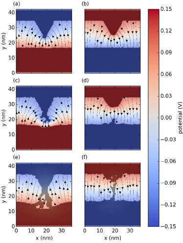
Figure 2 shows a typical simulated evolution of the junction at negative and positive tip potentials (left and right panels in Fig. 2, respectively). The structural development can be followed from the top to bottom panels. The initial asymmetrical arrangement, representing an STM tip - flat surface setup, develops in time very differently at opposite bias polarities. Figures 2(a) and 2(b) demonstrate that at the initial phase of the filament formation the region of the most intensive structural changes are located at the apex of the tip, where the electric field is the highest. At a negative tip potential the silver atoms are being deposited on the apex and a filament starts growing towards the bottom surface. Figure 2(c) illustrates a dendritic filament growth which is predominantly fueled by the oxidation of the silver atoms of the bottom electrode located under the filament. At a reversed polarity the tip gradually loses its apex leading to an effective shrinking while opposite filament growth starting from the flat surface toward the tip is taking place [Fig. 2(d)]. Figures 2(e) and 2(f) show the filament structures after establishing a metallic contact between the electrodes. Figure 2(e) demonstrates that the initial asymmetry of the contact is qualitatively preserved, while dendritic features in the filament and a shallow dip in the planar electrode also appear. These qualitative features are in remarkable agreement with in-situ experimental studies on the dynamics of nanoscale metallic inclusions in dielectrics Xu et al. (2010), where due to the high redox rates and ion mobility Yang et al. (2013) in stoichiometric Ag2S, qualitatively similar filament growth was observed.
Next we study the relation of the preserved asymmetry after complete filament formation to the observed, robustly uniform polarity of the resistive switchings taking place between metallic OFF and ON states, corresponding to our experimentally investigated configuration [Fig. 1]. We performed simulations starting from simplified asymmetric filament boundaries representing an STM tip - flat surface setup as illustrated in Figs. 3(a) and 3(b). Figures 3(c) and 3(d) demonstrate that under the influence of a negative (positive) tip bias the diameter of the filament increases (reduces) by time, in full agreement with the observed polarities of the set/reset transitions, underlining the fundamental role of the asymmetrical initial arrangement of the electrodes. The resulting electric field profiles reveal that the high field regions are located around the smallest cross-section of the contact, so that resistive switching can occur due to the increased probabilities of redox steps in the vicinity of the filament.
The simulated resistive states upon repeated biasing cycles are shown in Fig. 4. The two-terminal resistance is calculated from the bias voltage and the current through the contact which is where the integration is over the horizontal cross-section of the two-dimensional plane. Due to its reduced dimensionality, our simple model is not expected to provide a quantitative agreement with the experimentally observed resistance values nor to account for the closing of the hysteresis loops upon a biasing cycle. Nevertheless, calculating the two-terminal resistance by taking, as a rude estimate, the bulk conductivity of silver and the narrowest (one-dimensional) cross-section of the junction into account, the basic qualitative features of the hysteretic I-V traces can be reproduced.
In order to further verify the dominant role of the geometrical asymmetry in the polarity of the resistive switchings, we also performed experiments on sulfurized Ag-Ag junctions established in an MCBJ arrangement, as illustrated in the inset of Fig. 5. We note that our previous experiments Geresdi et al. (2011a) utilizing the MCBJ technique for creating clean Ag-Ag atomic junctions at room temperature also reproduced the main features of the usually observed resistive switching behavior which were attributed to electromigration taking place finite bias. However, in the absence of an ionic conductor layer these individual characteristics were highly unstable in spite of the superior mechanical stability offered by the MCBJ technique Muller et al. (1992) over the one of an off-feedback STM setup.
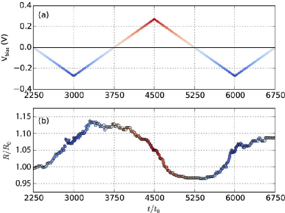
Unlike in the STM setup, where the initial asymmetry of the junction is largely predetermined by the different shapes of the thin film and sharp tip electrodes, the controlled rupture of a uniform wire is expected to result in a randomly oriented local asymmetry at the apex of the nanojunction. In our present experiments stable, hysteretic I-V traces exhibiting comparable, metallic ON and OFF state resistances but opposite switching polarities were obtained after sulfurisation and controlled re-connection of the freshly created Ag-Ag junctions, as exemplified in Fig. 5. The statistical analysis of 10 identically prepared samples revealed a 50% probability of having a set/reset transition at a given voltage polarity independently from the applied bias during re-connection, providing an excellent agreement with our qualitative scenario. When a stable sequence of I-V measurements was followed by a complete rupture and re-connection of the electrodes, the polarity of the subsequent switchings were likely (80%) to be identical to those obtained previously, indicating that up to a certain degree of re-establishment the asymmetry of the junction is mostly determined by the first rupture and is robust against repeated mechanical reconfigurations.
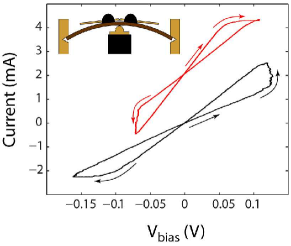
Based on the above findings we studied resistive switchings also in a series of prototype on-chip memory devices illustrated in the inset of Fig. 6. The structure mimicking the asymmetry of the STM arrangement was patterned by standard electron beam lithography on an amorphous, 140 nm thick SiNx substrate. The 100 nm wide and 45 nm thick, electron beam evaporated silver channel connecting the electrodes was further reduced in its diameter by controlled electromigration in vacuum conditions Strachan et al. (2005); Esen and Fuhrer (2005); Nef et al. (2014). During the electromigration process the junction was exposed to a series of 0.5 ms long voltage pulses of increasing amplitude ranging from 10 mV to a maximum of 300 mV. The sample’s resistance was monitored during the 100 ms dwell time between the pulses by acquiring low bias I-V traces. By repeating this method, the typical starting resistance of 50 could be increased to 250 . At this setpoint the bias was removed and due to a self-breaking mechanism O’Neill et al. (2007); Prins et al. (2009) an approximately 1 nm wide gap opened at the narrowest cross-section of the silver channel situated presumably close to the apex of the triangular electrode, as suggested by the inset of Fig. 6. This nanogap was then exposed to vaporized sulfur at 60∘C at ambient pressure followed by the re-connection of the electrodes by triangular voltage signals up to 2 V amplitudes. An optimized, 3 minutes long sulfurisation time resulted stable, hysteretic I-V traces highly similar to those obtained by the previously discussed techniques, also reflecting identical switching polarities as exemplified in Fig. 6. This effect is attributed to the formation of a few 10 nm long region of Ag2S where filament formation and destruction can take place between the electrodes during memory operations. While the endurance of these very first proof of concept devices were in the order of a few 100 cycles we believe that, owing to their largely simplified structure and inherently high mechanical stability, the future optimization of the design and fabrication parameters is expected to enable the reliable application of such memory architectures.
The reproducibility of the measured I-V traces at stable junction configurations are illustrated in Figs. 7(a), 7(b) and 7(c) for STM, MCBJ and lithographically designed on-chip structures, respectively. The evaluated average and values deduced from the curves shown in Fig. 7(a) and their 10% relative standard deviation comply with those obtained in similarly established PtIr-Ag2S-Ag nanojunctions Gubicza et al. (2015b) and are limited by the long-term mechanical stability of our off-feedback STM setup Gubicza et al. (2015a). The superior mechanical stability of the MCBJ setup over the one of the off-feedback STM is reflected in the reduced relative standard deviations of the and values in Fig. 7(b). While the STM and MCBJ setups were installed by implementing advanced isolation techniques against mechanical vibrations, the I-V measurements of the lithographic structures were carried out in a mechanically undamped vacuum chamber which was installed directly at the inlet of a turbomolecular pump. Yet, the lowest dispersion of the and values was achieved in this setup [Fig. 7(c)], demonstrating the inherently high mechanical stability and robustness of our simplified on-chip design.
In conclusion, we investigated stable resistive switchings in Ag-Ag2S-Ag nanojunctions lacking the conventionally employed inert electrode. Our experiments performed in the STM and MCBJ arrangements demonstrated that the polarity of the set/reset transitions are exclusively determined by the inhomogeneity of the local electric field, arising from the geometrical asymmetry present at the apex of the junction. Numerical simulations taking activated ion migration and redox reactions into account successfully reproduced the observed switching behavior also in the so-far-less-widely-investigated metallic regime. The simulations also reveal that the atomic re-arrangements responsible for the observed resistive switchings only involve a small amount of silver ions situated in the vicinity of the junction’s narrowest cross-section providing a key ingredient to ultrafast memory operation Geresdi et al. (2014). Our proof of principle experiments demonstrate the merits of lithographically designed Ag-Ag2S-Ag nanostructures as fast and highly integrable memory cells. Additionally, by further optimization of the nanometer-scale, planar on-chip design, an inherently high mechanical stability is envisioned, whereas the utilization of all-Ag electrodes makes the lithographical fabrication procedure uncomplicated.
This work was supported by the Hungarian Research Funds OTKA K105735, K112918, the EC FP7 “CoSpinNano” (project No. 293797) and ITN “MOLESCO” (project No. 606728) and by the UK EPSRC grants EP/K001507/1, EP/J014753/1 and EP/H035818/1. Useful discussions with Z. Balogh, B. Fülöp and M. Calame are acknowledged. The experimental data is held by the Department of Physics, Budapest University of Technology and Economics. The underlying data for the theory analysis is available in the Appendix.
*
Appendix A Appendix: The numerical simulations
In order to qualitatively investigate the silver filament growth in Ag-Ag2S-Ag structures we performed atomic scale two-dimensional lattice based simulations. The simulation is implemented on an equilateral triangular lattice where a site can represent an empty site, a silver atom or a mobile silver ion. The presence of sulphide ions is taken into account as a screening medium reducing the range of the silver ion interactions to nearest neighbor. The microscopic development is driven by room temperature ionic diffusion and redox processes, the latter taking place at the electrode surfaces. Similar filament growth simulations have been done before in Ref. 52 utilizing different theoretical models.
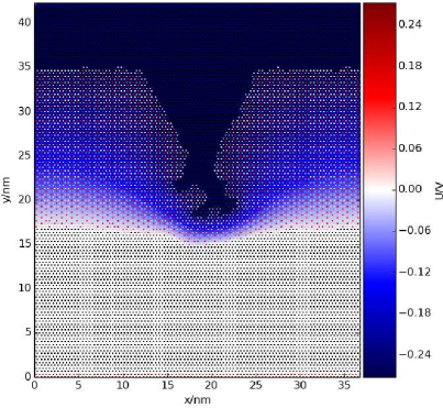
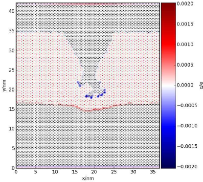
A typical equilateral triangular lattice used in the simulations can be recognized in Fig. A1 where the black dots denote silver atoms, the red dots represent silver ions. The lattice exhibits periodic boundary conditions along the horizontal direction while the vertical boundaries are terminated by two layers of silver atoms set to and zero potentials on the top and bottom, respectively. The lattice constant is set to =3.85 which approximately corresponds to one real atom per site. The electrostatic potential on each site is computed by solving the Poisson’s equation on the lattice. The charges of the silver ions are considered to be screened, therefore they are excluded from the electrostatic calculation. is set to zero outside, whereas inside the silver is applied. The surface charge density is computed from the potential as .
The time development is performed either by moving some of the silver ions or atoms to their neighboring empty site or by simulating a redox reaction, in which silver ions and atoms located at an electrode surface are exchanged. First the electrostatic potential is computed in each time step. This is followed by the calculation of a transition probability for each possible change. Finally the changes are executed with the calculated probabilities. The transition probability of a silver ion at site moving to its neighboring empty site is computed as Domb et al. (1995)
where is the energy change of the move, is the attempt frequency of the silver ion to jump and is the duration of the time steps. The transition probability of a silver atom jumping from site to its neighboring empty site is computed similarly using and . The transition probability for a redox step, where a surface silver atom on site is oxidized and a surface silver ion on site is reduced, is computed as
where is the energy change due to the oxidation and reduction on site and site , respectively, and is the redox reaction rate. The duration of the time steps is chosen such that the typical transition probability is much smaller than 1. The energy changes are calculated as
where the electrochemical potential of a silver ion at site is
where and are the numbers of silver ion and atom neighbors of site , respectively, and are the interaction energies, is the charge of the silver ion and is the potential at site . The electrochemical potential for the silver atom is
where the is the interaction energy between silver atoms. The sites and denote neighboring silver sites to and , respectively. They are chosen to provide the maximum probability for the given redox reaction. The electron’s electrochemical potential on a surface site is calculated as Bernard et al. (2003)
where is the charge density at the surface site and is the surface density of states in silver. The structural evolution of the contact is determined by the locations of the redox processes. The above formulae of the chemical potential imply that the typical locations of the redox reactions are determined by the average numbers of neighbors i.e., the ion concentration, and by the surface charge density. The numbers of neighbors are weighted with the interaction energies, therefore this contribution is coupled to the energetics of the diffusion process, whereas the surface charge density terms depend on the metal properties.
The typical parameter values utilized in the simulations were =0.001, =0.01, =3, =2, =-20, , =10, and the concentrations of mobile silver ions, . Adjusting the parameter values two extreme scenarios may take place: the initial structure either explodes or no significant change occurs during the simulated timescale. Trying different parameter sets to avoid such extreme outcomes, we found that resistive switching is a robust phenomenon in the simulated memristor structures which does not require fine tuning of the parameters. Increasing the voltage bias or reducing the strength of the silver-silver interactions can lead to more dendritic evolvement and also the structure more likely explodes to a random mixture of atoms and ions. The parameter provides a means to increase the probability of redox reactions without tuning the diffusion parameters.
A snapshot of the electrostatic potential and surface charge density maps corresponding to a dendritic filament formation are displayed along with the underlying lattice in high resolution in Figs. A1 and A2, respectively. Two animation files are also added to the present paper. Animation 1 shows the structural evolution during silver filament formation in an asymmetrical tip - flat surface electrode arrangement, as explained via the snapshots displayed in Fig. 2. Animation 2 shows the modulation in the width of a completed metallic filament having asymmetrical boundaries (as seen in Fig. 3) under bias voltages of alternating sign.
References
- Yang et al. (2013) J. J. Yang, D. B. Strukov, and D. R. Stewart, Nat. Nano 8, 13 (2013).
- Borghetti et al. (2010) J. Borghetti, G. S. Snider, P. J. Kuekes, J. J. Yang, D. R. Stewart, and R. S. Williams, Nature 464, 873 (2010).
- Pershin and Di Ventra (2011a) Y. V. Pershin and M. Di Ventra, Phys. Rev. E 84, 046703 (2011a).
- Terabe et al. (2005) K. Terabe, T. Hasegawa, T. Nakayama, and M. Aono, Nature 433, 47 (2005).
- Strukov et al. (2008) D. B. Strukov, G. S. Snider, D. R. Stewart, and R. S. Williams, Nature 453, 80 (2008).
- Waser and Aono (2007) R. Waser and M. Aono, Nat. Mater. 6, 833 (2007).
- Terabe et al. (2007) K. Terabe, T. Hasegawa, C. Liang, and M. Aono, Adv. Mater. 8, 536 (2007).
- Wang et al. (2007) Z. Wang, T. Kadohira, T. Tada, and S. Watanabe, Nano Lett. 7, 2688 (2007).
- Jo and Lu (2008) S. H. Jo and W. Lu, Nano Lett. 8, 392 (2008).
- Aono and Hasegawa (2010) M. Aono and T. Hasegawa, IEEE Proc. 898, 2228 (2010).
- Chung et al. (2010) A. Chung, J. Deen, J.-S. Lee, and M. Meyyappan, Nanotechnology 21, 412001 (2010).
- Linn et al. (2010) E. Linn, R. Rosezin, C. Kugeler, and R. Waser, Nat. Mater. 9, 403 (2010).
- Pershin and Di Ventra (2011b) Y. V. Pershin and M. Di Ventra, Adv. Phys. 60, 145 (2011b).
- Valov et al. (2011) I. Valov, R. Waser, J. R. Jameson, and M. N. Kozicki, Nanotechnology 22, 254003 (2011).
- Torrezan et al. (2011) A. C. Torrezan, J. P. Strachan, G. Medeiros-Ribeiro, and R. S. Williams, Nanotechnology 22, 485203 (2011).
- Hasegawa et al. (2012) T. Hasegawa, K. Terabe, T. Tsuruoka, and M. Aono, Adv. Mater. 24, 252 (2012).
- Chua (1971) L. Chua, IEEE Trans. Circuit Theory 18, 507 (1971).
- Gubicza et al. (2015a) A. Gubicza, M. Csontos, A. Halbritter, and G. Mihály, Nanoscale 7, 4394 (2015a).
- Chang et al. (2011) T. Chang, S.-H. Jo, and W. Lu, ACS Nano 5, 7669 (2011).
- Ohno et al. (2011) T. Ohno, T. Hasegawa, T. Tsuruoka, K. Terabe, J. K. Gimzewski, and M. Aono, Nat. Mater. 10, 591 (2011).
- Wagenaar et al. (2012) J. J. T. Wagenaar, M. Morales-Masis, and J. M. van Ruitenbeek, J. Appl. Phys. 111, 014302 (2012).
- Strukov and Williams (2008) D. B. Strukov and R. S. Williams, Appl. Phys. A 94, 515 (2008).
- Xu et al. (2010) Z. Xu, Y. Bando, W. Wang, X. Bai, and D. Golberg, ACS Nano 4, 2515 (2010).
- Nayak et al. (2010) A. Nayak, T. Tamura, T. Tsuruoka, K. Terabe, S. Hosaka, T. Hasegawa, and M. Aono, J. Phys. Chem. Lett. 1, 604 (2010).
- Morales-Masis et al. (2009) M. Morales-Masis, S. J. van der Molen, W. T. Fu, M. B. Hesselberth, and J. M. van Ruitenbeek, Nanotechnology 20, 095710 (2009).
- Morales-Masis et al. (2010) M. Morales-Masis, H.-D. Wiemhöfer, and J. M. van Ruitenbeek, Nanoscale 2, 2275 (2010).
- Morales-Masis et al. (2011) M. Morales-Masis, S. J. van der Molen, T. Hasegawa, and J. M. van Ruitenbeek, Phys. Rev. B 84, 115310 (2011).
- Nayak et al. (2011) A. Nayak, T. Tsuruoka, K. Terabe, T. Hasegawa, and M. Aono, Appl. Phys. Lett. 98, 233501 (2011).
- Menzel et al. (2012) S. Menzel, U. Böttger, and R. Waser, J. Appl. Phys. 111, 014501 (2012).
- Valov et al. (2012) I. Valov, I. Sapezanskaia, A. Nayak, T. Tsuruoka, T. Bredow, T. Hasegawa, G. Staikov, M. Aono, and R. Waser, Nat. Mater. 11, 530 (2012).
- Yang et al. (2012) Y. Yang, P. Gao, S. Gaba, T. Chang, X. Pan, and W. Lu, Nat. Comm. 3, 732 (2012).
- Liu et al. (2012) Q. Liu, J. Sun, H. Lv, S. Long, K. Yin, N. Wan, Y. Li, L. Sun, and M. Liu, Adv. Mater. 24, 1844 (2012).
- Menzel et al. (2013) S. Menzel, S. Tappertzhofen, R. Waser, and I. Valov, Phys. Chem. Chem. Phys. 15, 6945 (2013).
- Yang and Lu (2013) Y. Yang and W. Lu, Nanoscale 5, 10076 (2013).
- Cheng and Hu (2015) P. Cheng and Y. H. Hu, J. Mater. Chem. C 3, 2768 (2015).
- Nardi et al. (2012) F. Nardi, S. Larentis, S. Balatti, D. C. Gilmer, and D. Ielmini, IEEE Trans. El. Dev. 59, 2461 (2012).
- Larentis et al. (2012) S. Larentis, F. Nardi, S. Balatti, D. C. Gilmer, and D. Ielmini, IEEE Trans. El. Dev. 59, 2468 (2012).
- Mickel et al. (2014) P. R. Mickel, A. J. Lohn, C. D. James, and M. J. Marinella, Adv. Mater. 26, 4486 (2014).
- Geresdi et al. (2014) A. Geresdi, M. Csontos, A. Gubicza, A. Halbritter, and G. Mihály, Nanoscale 6, 2613 (2014).
- Gubicza et al. (2015b) A. Gubicza, M. Csontos, A. Halbritter, and G. Mihály, Nanoscale 7, 11248 (2015b).
- Yang et al. (2014) Y. Yang, P. Gao, L. Li, X. Pan, S. Tappertzhofen, S. Choi, R. Waser, I. Valov, and W. D. Lu, Nat. Comm. 5, 4232 (2014).
- Geresdi et al. (2011a) A. Geresdi, A. Halbritter, A. Gyenis, P. Makk, and G. Mihály, Nanoscale 3, 1504 (2011a).
- Schirm et al. (2013) C. Schirm, M. Matt, F. Pauly, J. C. Cuevas, P. Nielaba, and E. Scheer, Nat. Nano 8, 645 (2013).
- Johnson et al. (2010) S. L. Johnson, A. Sundararajan, D. P. Hunley, and D. R. Strachan, Nanotechnology 21, 125204 (2010).
- Muller et al. (1992) C. J. Muller, J. M. van Ruitenbeek, and L. J. de Jongh, Physica C 191, 485 (1992).
- Geresdi et al. (2011b) A. Geresdi, A. Halbritter, E. Szilágyi, and G. Mihály, MRS Proceedings 1331 (2011b).
- Strachan et al. (2005) D. R. Strachan, D. E. Smith, D. E. Johnston, T.-H. Park, M. J. Therien, D. A. Bonnell, and A. T. Johnson, Appl. Phys. Lett. 86, 043109 (2005).
- Esen and Fuhrer (2005) G. Esen and M. S. Fuhrer, Appl. Phys. Lett. 87, 263101 (2005).
- Nef et al. (2014) C. Nef, L. Pósa, P. Makk, W. Fu, A. Halbritter, C. Schönenberger, and M. Calame, Nanoscale 6, 7249 (2014).
- O’Neill et al. (2007) K. O’Neill, E. A. Osorio, and H. S. J. van der Zant, Appl. Phys. Lett. 90, 133109 (2007).
- Prins et al. (2009) F. Prins, T. Hayashi, B. J. A. de Vos van Steenwijk, B. Gao, E. A. Osorio, K. Muraki, and H. S. J. van der Zant, Appl. Phys. Lett. 94, 123108 (2009).
- Zhang et al. (2014) Y. Zhang, N. Islam Mou, P. Pai, and M. Tabib-Azar, in SENSORS, 2014 IEEE (IEEE, 2014), pp. 819–822.
- Domb et al. (1995) C. Domb, R. K. Zia, B. Schmittmann, and J. L. Lebowitz, Statistical mechanics of driven diffusive systems, vol. 17 (Academic Press, 1995).
- Bernard et al. (2003) M.-O. Bernard, M. Plapp, and J.-F. Gouyet, Phys. Rev. E 68, 011604 (2003).