Stripe and short range order in the charge density wave of 1T-CuTiSe
Abstract
We study the impact of Cu intercalation on the charge density wave (CDW) in 1T-CuTiSe by scanning tunneling microscopy and spectroscopy. Cu atoms, identified through density functional theory modeling, are found to intercalate randomly on the octahedral site in the van der Waals gap and to dope delocalized electrons near the Fermi level. While the CDW modulation period does not depend on Cu content, we observe the formation of charge stripe domains at low Cu content (x0.02) and a breaking up of the commensurate order into 22 domains at higher Cu content. The latter shrink with increasing Cu concentration and tend to be phase-shifted. These findings invalidate a proposed excitonic pairing as the primary CDW formation mechanism in this material.
Correlated electron systems are prone to develop distinct electronic ground states, such as superconductivity, charge density waves (CDWs), and spin ordered phases. The nature of the interplay between these ground states is the focus of intense research efforts. A CDW is a spatial modulation of the electron density associated with local lattice distortions. CDWs are found in a number of quasi-two-dimensional superconductors, including transition metal dichalcogenides Wilson et al. (1975), intercalated graphite Rahnejat et al. (2011), cuprates Howald et al. (2003); Chang et al. (2012); Ghiringhelli et al. (2012) and pnictides Rosenthal et al. (2014). Of particular interest, largely driven by the puzzle of high temperature superconductivity, is whether charge order is competing, cooperating or simply coexisting with superconductivity Keimer et al. (2015). The layered transition metal dichalcogenide 1T-TiSe offers an attractive playground to explore the interplay between these two electronic ground states, thus potentially contributing to resolving similar outstanding questions in cuprate superconductors and other strongly correlated materials.
1T-TiSe consists of a stack of van der Waals (vdW) coupled layers allowing in-situ preparation of surfaces ideally suited for scanning probe investigations by cleaving. When cooled below K, it undergoes a second-order phase transition into a commensurate 222 CDW superlattice Wilson and Yoffe (1969); Di Salvo et al. (1976). There is currently no consensus on the origin of the CDW in this material. Two possible scenarios are being considered, one based on a purely electronic process characterized by an excitonic instability Wilson and Yoffe (1969), while the other one involves a Jahn-Teller (JT) distortion Hughes (1977). More refined theories also propose a mixture of these two possible contributions, in the so called indirect JT transition Kidd et al. (2002); van Wezel et al. (2010); Phan et al. (2013).
1T-TiSe becomes superconducting when intercalating more than x=0.04 copper into the vdW gap, with a maximum critical temperature 4.1 K near x=0.08 Morosan et al. (2006). Transport measurements Morosan et al. (2006); Wu et al. (2007) indicate the CDW is suppressed upon increasing the Cu content which would suggest a competition with superconductivity. A more recent report of an incommensurate CDW above the superconducting dome in pristine crystals under pressure Joe et al. (2014) suggests a more complex scenario, where CDW fluctuations promote superconductivity. Traces of incommensurate CDW patches have also been found in gated TiSe thin films Li et al. (2016). Here, we focus on the effect of Cu intercalation on the CDW in 1T-TiSe in an effort to contribute to this discussion from an atomic scale structural and spectroscopic perspective.
The band structure is an important ingredient for understanding the CDW and superconducting phases. According to angular resolved photoemission (ARPES), the dominant contributions to the electronic band structure near the Fermi level are a Ti 3d conduction band at the L point and a Se 4p valence band at the point of the Brillouin zone Monney et al. (2010). At low temperature, ARPES reveals strong band renormalization with a large transfer of spectral weight into backfolded bands pointing at an excitonic ground state driven CDW transition. On Cu intercalated crystals, ARPES shows the Ti 3d conduction band to sink below the Fermi level, indicating an electron donor character of Cu. Increasing the Cu content towards the superconducting composition, the backfolding of the Se 4p valence band is found to slowly disappear, suggesting competition between CDW order and superconductivity Qian et al. (2007). However an alternative explanation contends that the latter is a coincidental response to increasing the chemical potential, which suppresses the CDW, and to the enhancement of states at the Fermi level that unltimately favors the emergence of superconductivity Zhao et al. (2007).
1T-CuTiSe (0x0.07) single crystals were grown by iodine vapour transport of a stoichiometric mixture of Ti and Se sealed in a quartz ampoule under high vacuum. The Cu content x was adjusted by adding an appropriate amount of metallic Cu to the starting materials. Single crystals were obtained after one week at 650∘C for pristine (x=0) and 830∘C for Cu intercalated specimen. These temperatures were chosen to limit the amount of Ti self doping Di Salvo et al. (1976); Hildebrand et al. (2016). The single crystals were cleaved in-situ at room temperature prior to the STM/STS measurements (base pressure below mBar). We used in-situ conditioned PtIr tips and the bias voltage V was applied to the sample. The differential conductance dI/dV(V) curves were acquired using a standard lock-in technique with a 5 mV bias modulation at 413.7 Hz.
DFT modeling of intercalated Cu was performed with the plane wave pseudopotential code VASP Kresse and Furthmuller (1996); Kresse and Hafner (1993), version 5.3.5. Projector-augmented waves Kresse and Joubert (1999) in a 28.0428.04 Å2 rhombohedral unit cell were used with the Perdew-Burke-Ernzerhof (PBE) Perdew et al. (1996) exchange correlation functional and plane wave cutoffs of 295 eV. The 1T-TiSe surface was modeled with two layers with the bottom Se layer fixed. A Monkhorst-Pack mesh with 111 and 221 k-points was used to sample the Brillouin zone of the cell, with the finer grid used to check convergence. The parameters gave an energy difference convergence better than 0.01 eV. During structural relaxations, a tolerance of 0.03 eV/Åwas applied. STM images were generated following the Tersoff-Hamann Tersoff and Hamann (1983) approach in which the I(V) characteristic measured by STM is proportional to the integrated local density of states (LDOS) of the surface using the BSKAN code Hofer (2003).
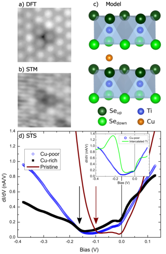
A positive identification of the Cu atoms in topographic STM images is paramount to a thorough atomic scale study of the impact of intercalated Cu on the CDW in 1T-CuTiSe. While STM imaging readily revealed specific patterns of intercalated Ti and three other dominant single atom defects in 1T-TiSe Hildebrand et al. (2014), the footprint of intercalated Cu proved far more elusive. Guided by DFT modeling, we find that intercalated Cu atoms are only resolved with atomic resolution in a reduced energy window around -1.2 V, with a perfect correspondence between model and data (Fig.1a,b). This is the first solid experimental evidence that intercalated Cu is indeed sitting on the octahedral site in the vdW gap (Fig.1c), as assumed in literature Titov et al. (2001); Stoltz et al. (2005).
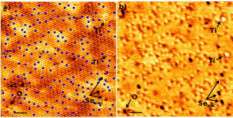
Substantial charge inhomogeneities are seen in STM micrographs of Cu intercalated 1T-TiSe (Fig.2a), especially at low bias. Imaging the exact same region at -1.2 V (Fig.2b) where Cu atoms can be resolved one by one, we show that these inhomogeneities are directly linked to intercalated Cu, with bright regions corresponding to an accumulation of Cu atoms. The two distinct STM images in Fig.2 have been aligned with atomic scale precision based on single atom defects identified in previous studies Hildebrand et al. (2014); Novello et al. (2015). Such precise identification of single atom defects resolved by STM permits exquisite insight into the microscopic nature of the material and the CDW. The atomic patterns of the defects associated with single atom O, I, Ti and Cu defects imply that the observed CDW modulation resides on the Se sites. The relative orientation of these mostly triangular features further confirm the local 1T-polytype of the single crystals investigated. Intercalated Ti was shown to show two different topographic patterns depending on its relative position with respect to the CDW superlattice Hildebrand et al. (2014). In the case of Cu, no topographic difference is seen instead. Finally, the local Cu concentration of the region under the STM tip can be assessed simply by counting the Cu atoms: the 200 Cu atoms found within the 1818 nm of Fig.2 are in excellent agreement with the nominal doping x=0.07 of that crystal.
Low temperature tunneling spectroscopy of 1T-CuTiSe (Fig.1d) reveals a gap 80 meV opening below the chemical potential as the material is cooled through for all Cu concentrations considered. This marked asymmetry and line shape are unusual for a CDW. Note that the gap opening below the Fermi level is consistent with the observed real space charge modulation residing primarily on the Se sites and Se 4p states being the main contributions to the valence band. The gap edge in the occupied LDOS is shifting to lower energies with increasing Cu content (arrows in Fig.1d) while the gap is partially filling with states added near the Fermi level. These spectral changes correspond to increasing the chemical potential consistent with the electron donor nature of intercalated Cu. They are sensitive to the local Cu concentration with a higher LDOS measured at in the brighter Cu-rich regions (Fig.2a and Fig.3)). These observations are in agreement with previous STM Iavarone et al. (2012) and ARPES Qian et al. (2007); Zhao et al. (2007) studies. Here, we demonstrate a direct link between the Cu content and the observed band shift. The origin of the weak singularity at , also observed in point-contact tunneling Luna et al. (2015), remains to be firmly established. It is most likely not a real DOS feature but a manifestation of electron-electron interaction and impurity scattering expected in disordered metals Al’Tshuler and Aronov (1979), with disorder due to intercalated Cu and Ti.
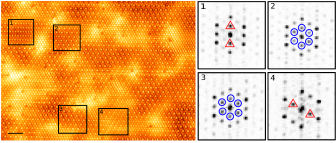
The charge order landscape imaged by STM in 1T-CuTiSe depends on the Cu content x. The most striking features in filled state STM micrographs of low doped crystals (x0.02) are the appearance of symmetry breaking stripe CDW (1Q) domains and, in Cu-rich regions, a reduced amplitude of the 22 CDW (3Q) (Fig.3a). Tip artifacts are excluded to explain the stripe domains: 1Q and 3Q charge order is seen along the same scan line - hence with the same tip configuration. We do not measure any systematic spectroscopic difference between the two domains. Stripe charge order has been observed by STM in other layered compounds Soumyanarayanan et al. (2013); Rahnejat et al. (2011); Bando et al. (1997) and was attributed to local strain. Strain could play a role here as a consequence of the reported 1T-TiSe unit cell expansion when intercalating Cu Shkvarin et al. (2016).
We observe 1Q and 3Q phases coexisting down to 1.2 K in low doped crystals. They are always commensurate and in perfect registry with the Se lattice. The Fourier transforms show the component of the stripe phase to be identical to one of the three components of the 3Q phase (Fig.3). This is different from the observations in 2H-NbSe where they were found to differ by as much as 13% Soumyanarayanan et al. (2013). The independence of the 1Q and 3Q Fourier components on Cu concentration and the marked electron-hole asymmetry of the CDW gap exclude a Fermi surface nesting mechanism to explain the CDW. Fig.3 further questions the chiral nature of the CDW in 1T-TiSe claimed in several STM studies Ishioka et al. (2010); Iavarone et al. (2012) based on a systematic hierarchy in the amplitudes of the CDW Fourier components. There is no supporting evidence for a chiral CDW in our images. We see no significant amplitude differences in the Fourier components, and only a single component is present in the stripe domains.
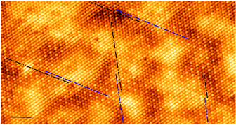
In high doped crystals (x0.05), we do not observe well developed stripe domains but we find the 3Q phase to break up into short range ordered nanometer-scale domains (Fig.4). These domains are predominantly surrounded by Cu-rich regions, and tend to be -phase shifted with a few atomically sharp boundaries separating adjacent domains. A similar break up of the CDW into phase-shifted domains has been reported recently in Ti intercalated crystals Hildebrand et al. (2016) where the effect is observed already for 2% Ti content. In both cases, the 22 domain size is shrinking with increasing number of intercalated atoms and the charge modulation period is independent of x.
Comparing the impact of Cu and Ti on the charge order and LDOS provides insightful clues on the CDW formation mechanism. Modeling the STM fingerprints of Cu (Fig.1) and Ti Hildebrand et al. (2014) shows they intercalate on the same lattice site in the vdW gap of 1T-TiSe. Both contribute electrons to the system. Ti is a local dopant with a broad localized state below the Fermi level in the tunneling spectra and no apparent shift in chemical potential (inset of Fig.1d). Cu on the other hand is a band dopant inducing a significant shift in the chemical potential (Fig.1d). The peak in the resistivity as a function of temperature at the CDW phase transition is progressively reduced with increasing Cu content while it collapses abruptly for the highest Ti content Hildebrand et al. (2016). These results can be understood within the exciton CDW formation mechanism. We have shown that increasing Cu gradually shifts the chemical potential up in energy (Fig.1d) and the Ti 3d band deeper below the Fermi level. The system thereby becomes metallic (see also Morosan et al. (2006)) and the formation of excitons is progressively suppressed. Ti doping on the other hand does not shift the chemical potential, leaving the excitonic pairing unchanged until the CDW domain size becomes smaller than the exciton Bohr radius thus abruptly suppressing their formation Hildebrand et al. (2016).
However, the exciton scenario is not compatible with the persistence of a clear local charge order observed by STM in crystals where the CDW phase transition is no longer detected by transport. Thus, excitons may enhance long-range CDW correlations resulting in a signal for non-local probes such as transport and ARPES, but the microscopic CDW formation must involve other contributions such as phonons, for example. A similar picture was proposed in a pump-probe study of 1T-TiSe Porer et al. (2014), where it was shown that the lattice distortion is still present when the excitonic order is quenched. Van Wezel et al. van Wezel et al. (2010) also concluded in a theoretical study that the presence of excitons significantly enhances the CDW order induced by electron phonon coupling. In addition, the gap opening below the Fermi level as measured by tunneling spectroscopy renders a purely electronic mechanism energetically unfavorable.
Finally, and although superconductivity is not the main focus of this work, we note that the persistence of well developed CDW domains up to the highest Cu contents considered suggests that the suppression of the CDW is not the key factor in the emergence of superconductivity in 1T-CuTiSe. Instead, as already proposed in high-pressure Joe et al. (2014) and carrier injection Li et al. (2016) experiments, superconductivity may arise from the inhomogeneities of the CDW pattern. Moreover, spectroscopy shows Cu intercalation to shift the chemical potential to higher energies and increase the LDOS at the Fermi level providing a favorable electronic configuration for the appearance of superconductivity above x=0.04.
In summary, the unambiguous identification of intercalated Cu atoms in 1T-TiSe enables us to specify their precise atomic position in the octahedral site of the vdW gap - unknown so far - and to establish a firm link between Cu doping and STM topographic and spectroscopic features. In particular, we confirm Cu is a donor contributing delocalized electrons at the Fermi level and shifting the chemical potential up in energy in agreement with previous ARPES results Qian et al. (2007); Zhao et al. (2007). We observe a striking instability towards the formation of charge stripes at low Cu concentration (x0.02) and the formation of short-range ordered domains which tend to be phase-shifted at higher Cu contents (x0.05). The charge order period observed by STM imaging is independent on the nominal Cu concentration and persists locally to doping levels where transport and other spectroscopy techniques no longer detect a CDW phase. The present STM/STS study shows that excitonic pairing alone cannot account for the CDW formation and that another, not purely electronic microscopic mechanism must be at play.
This project was supported by the Swiss National Science Foundation through Div.II (grants 144139 and 162517). DFT calculations were performed using the LCN Computing Cluster. We acknowledge stimulating discussions with P. Aebi, B. Hildebrand, Ch. Berthod, J. van Wezel and J. Lorenzana. We thank C. Barreteau for her help with characterizing the single crystals via transport measurements and G. Manfrini and A. Guipet for their skillful technical assistance.
References
- Wilson et al. (1975) J. Wilson, F. D. Salvo, and S. Mahajan, Advances in Physics 24, 117 (1975).
- Rahnejat et al. (2011) K. Rahnejat, C. Howard, N. Shuttleworth, S. Schofield, K. Iwaya, C. Hirjibehedin, C. Renner, G. Aeppli, and M. Ellerby, Nat Commun 2, 558 (2011).
- Howald et al. (2003) C. Howald, H. Eisaki, N. Kaneko, and A. Kapitulnik, Proceedings of the National Academy of Sciences 100, 9705 (2003).
- Chang et al. (2012) J. Chang, E. Blackburn, A. T. Holmes, N. B. Christensen, J. Larsen, J. Mesot, R. Liang, D. A. Bonn, W. N. Hardy, A. Watenphul, M. v. Zimmermann, E. M. Forgan, and S. M. Hayden, Nat Phys 8, 871 (2012).
- Ghiringhelli et al. (2012) G. Ghiringhelli, M. Le Tacon, M. Minola, S. Blanco-Canosa, C. Mazzoli, N. B. Brookes, G. M. De Luca, A. Frano, D. G. Hawthorn, F. He, T. Loew, M. M. Sala, D. C. Peets, M. Salluzzo, E. Schierle, R. Sutarto, G. A. Sawatzky, E. Weschke, B. Keimer, and L. Braicovich, Science 337, 821 (2012).
- Rosenthal et al. (2014) E. P. Rosenthal, E. F. Andrade, C. J. Arguello, R. M. Fernandes, L. Y. Xing, X. C. Wang, C. Q. Jin, A. J. Millis, and A. N. Pasupathy, Nat Phys 10, 225 (2014).
- Keimer et al. (2015) B. Keimer, S. A. Kivelson, M. R. Norman, S. Uchida, and J. Zaanen, Nature 518, 179 (2015).
- Wilson and Yoffe (1969) J. Wilson and A. Yoffe, Advances in Physics 18, 193 (1969).
- Di Salvo et al. (1976) F. J. Di Salvo, D. E. Moncton, and J. V. Waszczak, Phys. Rev. B 14, 4321 (1976).
- Hughes (1977) H. P. Hughes, J. Phys. C: Solid State Phys. 10, L319 (1977).
- Kidd et al. (2002) T. E. Kidd, T. Miller, M. Y. Chou, and T.-C. Chiang, Phys. Rev. Lett. 88, 226402 (2002).
- van Wezel et al. (2010) J. van Wezel, P. Nahai-Williamson, and S. S. Saxena, Phys. Rev. B 81, 165109 (2010).
- Phan et al. (2013) V.-N. Phan, K. W. Becker, and H. Fehske, Phys. Rev. B 88, 205123 (2013).
- Morosan et al. (2006) E. Morosan, H. W. Zandbergen, B. S. Dennis, J. W. G. Bos, Y. Onose, T. Klimczuk, A. P. Ramirez, N. P. Ong, and R. J. Cava, Nat Phys 2, 544 (2006).
- Wu et al. (2007) G. Wu, H. X. Yang, L. Zhao, X. G. Luo, T. Wu, G. Y. Wang, and X. H. Chen, Phys. Rev. B 76, 024513 (2007).
- Joe et al. (2014) Y. I. Joe, X. M. Chen, P. Ghaemi, K. D. Finkelstein, G. A. de la Pena, Y. Gan, J. C. T. Lee, S. Yuan, J. Geck, G. J. MacDougall, T. C. Chiang, S. L. Cooper, E. Fradkin, and P. Abbamonte, Nat Phys 10, 421 (2014).
- Li et al. (2016) L. J. Li, E. C. T. O’Farrell, K. P. Loh, G. Eda, B. Özyilmaz, and A. H. Castro Neto, Nature 529, 185 (2016).
- Monney et al. (2010) C. Monney, E. F. Schwier, M. G. Garnier, N. Mariotti, C. Didiot, H. Cercellier, J. Marcus, H. Berger, a. N. Titov, H. Beck, and P. Aebi, New Journal of Physics 12 P, 125019 (2010).
- Qian et al. (2007) D. Qian, D. Hsieh, L. Wray, E. Morosan, N. L. Wang, Y. Xia, R. J. Cava, and M. Z. Hasan, Phys. Rev. Lett. 98, 117007 (2007).
- Zhao et al. (2007) J. F. Zhao, H. W. Ou, G. Wu, B. P. Xie, Y. Zhang, D. W. Shen, J. Wei, L. X. Yang, J. K. Dong, M. Arita, H. Namatame, M. Taniguchi, X. H. Chen, and D. L. Feng, Phys. Rev. Lett. 99, 146401 (2007).
- Hildebrand et al. (2016) B. Hildebrand, T. Jaouen, C. Didiot, E. Razzoli, G. Monney, M.-L. Mottas, A. Ubaldini, H. Berger, C. Barreteau, H. Beck, D. R. Bowler, and P. Aebi, Phys. Rev. B 93, 125140 (2016).
- Kresse and Furthmuller (1996) G. Kresse and J. Furthmuller, Phys. Rev. B 54, 11169 (1996).
- Kresse and Hafner (1993) G. Kresse and J. Hafner, Phys. Rev. B 47, 558 (1993).
- Kresse and Joubert (1999) G. Kresse and D. Joubert, Phys. Rev. B 59, 1758 (1999).
- Perdew et al. (1996) J. P. Perdew, K. Burke, and M. Ernzerhof, Phys. Rev. Lett. 77, 3865 (1996).
- Tersoff and Hamann (1983) J. Tersoff and D. R. Hamann, Phys. Rev. Lett. 50, 1998 (1983).
- Hofer (2003) W. Hofer, Progress in Surface Science 71, 147 (2003).
- Hildebrand et al. (2014) B. Hildebrand, C. Didiot, A. M. Novello, G. Monney, A. Scarfato, A. Ubaldini, H. Berger, D. R. Bowler, C. Renner, and P. Aebi, Phys. Rev. Lett. 112, 197001 (2014).
- Titov et al. (2001) A. N. Titov, A. V. Kuranov, V. G. Pleschev, Y. M. Yarmoshenko, M. V. Yablonskikh, A. V. Postnikov, S. Plogmann, M. Neumann, A. V. Ezhov, and E. Z. Kurmaev, Phys. Rev. B 63, 035106 (2001).
- Stoltz et al. (2005) S. E. Stoltz, H. I. Starnberg, and L. J. Holleboom, Phys. Rev. B 71, 125403 (2005).
- Novello et al. (2015) A. M. Novello, B. Hildebrand, A. Scarfato, C. Didiot, G. Monney, A. Ubaldini, H. Berger, D. R. Bowler, P. Aebi, and C. Renner, Phys. Rev. B 92, 081101 (2015).
- Iavarone et al. (2012) M. Iavarone, R. Di Capua, X. Zhang, M. Golalikhani, S. A. Moore, and G. Karapetrov, Phys. Rev. B 85, 155103 (2012).
- Luna et al. (2015) K. Luna, P. M. Wu, J. S. Chen, E. Morosan, and M. R. Beasley, Phys. Rev. B 91, 094509 (2015).
- Al’Tshuler and Aronov (1979) B. Al’Tshuler and A. Aronov, Soviet Journal of Experimental and Theoretical Physics 50, 968 (1979).
- Soumyanarayanan et al. (2013) A. Soumyanarayanan, M. M. Yee, Y. He, J. van Wezel, D. J. Rahn, K. Rossnagel, E. W. Hudson, M. R. Norman, and J. E. Hoffman, Proceedings of the National Academy of Sciences 110, 1623 (2013).
- Bando et al. (1997) H. Bando, Y. Miyahara, H. Enomoto, and H. Ozaki, Surface Science 381, L609 (1997).
- Shkvarin et al. (2016) A. S. Shkvarin, Y. M. Yarmoshenko, M. V. Yablonskikh, A. I. Merentsov, E. G. Shkvarina, A. A. Titov, Y. M. Zhukov, and A. N. Titov, The Journal of Chemical Physics 144, 074702 (2016), http://dx.doi.org/10.1063/1.4941767.
- Ishioka et al. (2010) J. Ishioka, Y. H. Liu, K. Shimatake, T. Kurosawa, K. Ichimura, Y. Toda, M. Oda, and S. Tanda, Phys. Rev. Lett. 105, 176401 (2010).
- Porer et al. (2014) M. Porer, U. Leierseder, J.-M. Ménard, H. Dachraoui, L. Mouchliadis, I. E. Perakis, U. Heinzmann, J. Demsar, K. Rossnagel, and R. Huber, Nat Mater 13, 857 (2014).