Mechanisms for strong anisotropy of in-plane g-factors in hole based quantum point contacts
Abstract
In-plane hole g-factors measured in quantum point contacts based on p-type heterostructures strongly depend on the orientation of the magnetic field with respect to the electric current. This effect, first reported a decade ago and confirmed in a number of publications, has remained an open problem. In this work, we present systematic experimental studies to disentangle different mechanisms contributing to the effect and develop the theory which describes it successfully. We show that there is a new mechanism for the anisotropy related to the existence of an additional effective Zeeman interaction for holes, which is kinematically different from the standard single Zeeman term considered until now.
pacs:
71.70.Ej, 73.22.Dj, 71.18.+yA quantum point contact (QPC) is a narrow quasi-one-dimensional (1D) constriction linking two two-dimensional (2D) electron or hole reservoirs. Experimental studies of QPCs started with the discovery of the conductance quantization in steps of Wees1988 ; Wharam1988 . The steps are due to the quantization of transverse channels Buttiker1990 . Effects of many-body correlations in QPCs were identified by a “0.7-anomaly” in the conductance, an enhancement of the g-factor in the 1D limit Thomas1996 , and by a zero bias anomaly Cronenwett2002 . G-factors in n-type QPCs have been measured in numerous experiments; a relatively recent one is reported in Ref. Burke2012 .
The in-plane electron g-factor in a QPC takes the same value for any direction of the in-plane magnetic field. Even in InGaAs, which has appreciable spin-orbit coupling, no in-plane g-factor anisotropy has been observed martin . Contrary to this, measurements for holes in QPCs based on GaAs p-type heterostructures indicate a huge anisotropy. All previously reported values of the g-factor for magnetic fields applied perpendicular to the QPC are consistent with within experimental error, while the g-factor for the parallel direction is nonzero chen ; komijani ; nichele .
Regardless of numerous studies, the g-factor anisotropy effect in QPCs remains unclear. One mechanism to explain the g-factor anisotropy was suggested in Ref. komijani . This mechanism is based on the crystal anisotropy of the cubic lattice. While it is not negligible, the contribution of this mechanism is too small to explain the observed anisotropy.
In this work, we identify a new mechanism for the g-factor anisotropy unrelated to the crystal lattice. It is instructive to use classification in powers of crystal anisotropy defined below. The new mechanism is leading in and the mechanism komijani is subleading. The new mechanism is negligible at very low hole densities. However, at real physical densities it is the major anisotropy mechanism. Previous measurements were performed in 2D hole systems formed at a single heterojunction chen ; komijani , which can be modeled as a triangular potential well. There is also a measurement with an asymmetric quantum well nichele which can be modeled as a square potential with an electric field along the z-axis. The z-axis is perpendicular to the plane of the 2D hole system. The z-asymmetry results in the cubic Rashba spin orbit interaction (SOI) Rashba ; chesi ; culcer ; nichele2 . We will show that there are two major mechanisms for suppression, (i) the -mechanism, (ii) the Rashba mechanism. To disentangle the mechanisms, in the present work we perform measurements of QPC g-factors for quantum well GaAs heterostructures which allows us to tune the Rashba SOI. By reducing the Rashba SOI we observe a non-zero for the first time (although the anisotropy is still large, with ). In all previous measurements the strong asymmetry of the heterostructure, or the high hole density resulted in a very strong Rashba SOI, so both mechanisms contributed to suppression of . The Rashba mechanism is not significant in our devices. (The mechanism is explained in the very end of the paper and discussed in detail in the supplementary material D.) The hole gas is confined in a 15nm rectangular quantum well. An external electric field is superimposed on the well using an in-situ back gate below the quantum well.
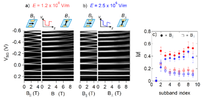
The transconductance maps measured at V/m and V/m are presented in Fig.1a,b. The absolute values of the g-factors extracted from these maps are shown in Fig.1c. All experimental details are provided in Section A of the supplementary material, see also Refs. ClarkeJAP06 ; Nextnano ; PatelPRB91 . Fig.1 demonstrates a significant g-factor anisotropy. Another observation is that in all cases both g-factors are very small for the lowest transverse channel, .
Dynamics of a single hole in bulk conventional semiconductors are described by the Luttinger Hamiltonian luttinger . We consider here the spherical approximation baldereshi
| (1) |
where is the 3D quasi-momentum; is the spin ; , are Luttinger parameters; is the free electron mass. There is also a non-spherical part of the Luttinger Hamiltonian that depends on the cubic lattice orientation. This part is proportional to . The parameter is small in compounds with large SOI, for example in GaAs and in InAs. In Ref. komijani a mechanism of the QPC g-factor asymmetry due to the non-spherical part of the Luttinger Hamiltonian was suggested. The contribution of this mechanism is small and is calculated in Section B of the supplementary material, see also Refs. Miserev1 ; simion ; Marie . Here we concentrate on the leading contribution which arises from the spherical Hamiltonian (1).
A quantum well potential imposed on (1) confines dynamics along the z-axis leading to 2D subbands. Here, we consider only the lowest sub-band with dispersion
| (2) |
where is the 2D momentum. At the projection of spin on the z-axis is a good quantum number. Due to the negative sign of the second term in (1), the lowest band is a Kramers doublet with . The standard way to describe the Kramers doublet is to introduce the effective spin with related Pauli matrices . The correspondence at is very simple: , . Note that the effective spin operators flip projections. Hence, are transformed as .
Now we apply in-plane magnetic field . The kinematic structure of the effective 2D Zeeman Hamiltonian is of the form Miserev1
| (3) |
Pauli matrices () have the angular momentum selection rule , and corresponds to . The powers of in (Mechanisms for strong anisotropy of in-plane g-factors in hole based quantum point contacts) balance the z-component of the angular momentum in such a way that the total Hamiltonian conserves the angular momentum, . While the -term in (Mechanisms for strong anisotropy of in-plane g-factors in hole based quantum point contacts) is well known, the -term has never been considered before. In perturbative treatment of the Luttinger Hamiltonian (1) the -term appears only in a high order of the perturbation theory. Of course, at small momenta , practically this is true if , where d is the width of the well. However, all experiments we are aware of (including ours) are performed at . In this case and are comparable.
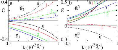
The functions and have been calculated recently for symmetric heterostructures Miserev1 . Here we calculate them for asymmetric ones. These functions for an infinite rectangular GaAs quantum well of width nm with superimposed electric field are plotted in Fig.2a.
Remarkably the existence of two isotropic g-functions leads to an anisotropy of the QPC g-factor. The QPC g-factor is determined experimentally by the splitting of the transconductance peaks in a magnetic field, see Fig.1. We define the x-axis to be along the QPC (the direction of the current) and the y-axis perpendicular to the QPC. The transconductance peaks correspond to the chemical potential aligning with the 1D subband edges, where . Therefore, in the g-factor measurements and . Hence, at the 1D subband edge the Zeeman interaction (Mechanisms for strong anisotropy of in-plane g-factors in hole based quantum point contacts) for a QPC reads
| (4) | |||
The superscript indicates that these are terms of the zero order in . Plots of and for an infinite 15nm rectangular GaAs quantum well with different values of are presented in Fig.2b.
Calculations of the in-plane Zeeman response have a nontrivial pitfall related to gauge invariance. This pitfall was overlooked in previous studies. To find the g-functions we diagonalize the 3D Hamiltonian
| (5) |
where is the vector potential included in via “long derivatives” (for details see Ref. Miserev1 ), and is the bulk g-factor. In Eq.(Mechanisms for strong anisotropy of in-plane g-factors in hole based quantum point contacts) is an arbitrary constant. Due to gauge invariance, cannot affect any physical observable. However, at arbitrary the minimum of the 2D hole dispersion is generally not at . In particular, in this situation the transconductance peaks do not correspond to . To avoid this complication we fix the value of with the condition that the minimum of the dispersion is at . For a symmetric quantum well the value of is dictated by symmetry, , the center of symmetry of the well. In the next paragraph we discuss how to determine for an asymmetric heterostructure, .
An asymmetric quantum well gives rise to Rashba SOI
| (6) |
This term has to be added to the effective 2D Hamiltonian given by Eqs.(2),(Mechanisms for strong anisotropy of in-plane g-factors in hole based quantum point contacts). Besides the Rashba SOI (6) one more kinematic structure in the effective 2D Hamiltonian is possible
| (7) |
Here, is a momentum dependent coefficient. To the best of our knowledge, the term (7) was unknown in previous literature. The momentum independent part of can be gauged out, see below, hence and scales as similar to (6). According to our calculations, (6) and (7) become comparable at T. Note that (6) and (7) are the only inversion asymmetric kinematic structures allowed by other symmetries in the effective 2D Hamiltonian in the spherical () approximation. The term (7) can be absorbed in the dispersion, , where and is the effective mass. This shift is equivalent to the variation of discussed in the previous paragraph. To fix the dispersion minimum at one needs to set . The value of providing this condition follows from the equation
| (8) |
Here is given by Eq.(Mechanisms for strong anisotropy of in-plane g-factors in hole based quantum point contacts) and is the effective 2D Hamiltonian which includes terms (2),(Mechanisms for strong anisotropy of in-plane g-factors in hole based quantum point contacts),(6) and (7). Brackets stand for the averaging over the wave function corresponding to , but . Solving Eq.(8) in the linear in B approximation yields the value of . The effect of quantum well asymmetry on the 2D functions , , and the 1D g-factors and calculated with the constraint (8) for electric fields MV/m are shown in Fig. 2 by the coloured lines. The corresponding values of determined from Eq.(8) are (zero is in the center of the square well).
To complete the discussion of gauge invariance, we would like to demonstrate that in the presence of the Rashba interaction (6) the functions and in Eq.(Mechanisms for strong anisotropy of in-plane g-factors in hole based quantum point contacts) are not gauge invariant. Let us perform the shift gauge transformation , . Hence the dispersion (2) is changed as . The term in this equation can be transferred to Eq.(7) leading to a change of that is discussed in the previous paragraph. One must also perform the shift of in the Rashba interaction (6), . The term in this equation can be transferred to Eq.(Mechanisms for strong anisotropy of in-plane g-factors in hole based quantum point contacts), leading to the change , . Here is the derivative of the Rashba coupling coefficient. Thus, the functions and are not gauge invariant. Of course, physical g-factors are gauge invariant, but generally they are different from , . Only in the gauge fixed by Eq.(8) the physical g-factors do coincide with , . The same is true for the subleading corrections and proposed in komijani and calculated in Section B of the supplementary material.
Our experiments have been performed with a 2D hole density of cm-2. It corresponds to a 2D Fermi momentum Å-1. The QPC channel is defined by the “transverse” Hamiltonian, , , where is the transverse self-consistent potential of the QPC. The energy levels of this Hamiltonian , enumerated by index , correspond to the 1D transverse channels. Varying the split-gate voltage adjusts the self-consistent potential , providing the condition to depopulate the 1D subband, . This implies that depends on n. The self-consistent potential for our device is calculated in Section C of the supplementary material using the Thomas-Fermi-Poisson method, see Refs. pyshkin ; davies ; modeling . The potentials for are plotted in Fig.3a.
While for the potential minimum in the 1D channel is practically zero, , for the value of is large, just slightly smaller than the Fermi energy. Therefore, in this case is much smaller than the Fermi momentum in the 2D reservoirs. Since the in-plane g-factors scale roughly as , the large value of explains the very small values of g-factors for , see Fig. 1c. Note that the potentials in Fig.3a are very close to those obtained a long time ago for electrons Laux . Note also that the behavior of g-factors at is different from that at and from , see Fig.1c. This is because of two competing and comparable effects, (i) the reduction of g-factors since , (ii) the enhancement of g-factors due to many body Coulomb interaction effects. The low n enhancement of the in-plane g-factor due to many body effects is well known in electron systems Thomas1996 . Fortunately, the both complications become irrelevant at . The condition holds, and the Coulomb interaction is sufficiently screened. The g-factors at can be determined from Fig. 2b by taking the values at . This gives the g-factors and shown by the dashed lines in Fig. 3b, plotted versus the applied electric field.
To complete the story we have also taken into account the subleading -correction due to crystal anisotropy proposed in Ref. komijani . We have corrected the calculations of Ref. komijani for some errors as described in the supplementary material. The -correction can be described by two momentum dependent functions and defined in Section B of the supplementary material. The -correction depends on the orientation of the QPC with respect to the crystal axes as given by Eq. (B7). In our experiment the QPC is oriented along the (110) direction, hence the angle defined by Eq.(B5) is . Therefore, according to (B7) and . The plots of versus electric field are presented in panel B of Fig.B1 in the supplementary material. Hence we arrive at the plots of and versus electric field shown in Fig.3b by the solid black and red lines. The calculated value of is practically independent of the field, and is equal to . In contrast, the perpendicular g-factor depends on the field significantly, and even changes sign. However, at values of the field used in the experiment, MeV/m and MeV/m the absolute values of the g-factor are practically equal, . The theory agrees with data presented in Fig.1. We stress that in there is no compensation between different contributions, therefore the calculation is rather reliable. On the other hand, for there is a significant compensation between the - and -contributions, therefore the expected theoretical uncertainty in is larger than that in .
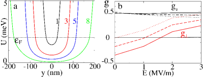
Dotted lines in Fig.3b show our prediction for the [100] orientation of the QPC. The essential ingredients of the theory are the functions , considered in the main text and the coefficients calculated in the supplementary material. In principle, one can disentangle these parameters experimentally by performing measurements for different with a set of QPCs aligned along different crystal orientations. Ideally the electric fields should encompass the values shown in Fig.3b, with QPC’s oriented along the [110] and [100] directions. All the devices must have the same density of holes in leads.
Besides the effect considered above, and the crystal anisotropy -correction calculated in Section B of the supplementary material, there is one more effect influencing . This 1D effect is due to a combination of the transverse QPC confinement with the Rashba SOI. It was previously addressed in numerical calculations for hole Gelabert and electron kolasinski wires. The 1D effect leads to oscillations and suppression with subband number , , where is a parameter related to the Rashba SOI. At the same time, is not affected. This effect is weak in quantum wells, and hence is irrelevant for our experiments, but is relevant in other experiments chen ; komijani ; nichele . The effect is discussed in Section D of the supplementary material.
In conclusion We have performed systematic experimental and theoretical studies to resolve the problem of anisotropic g-factors measured in quantum point contacts based on p-type heterostructures. We found that the most important mechanism for the anisotropy is related to the existence of two kinematically different effective Zeeman interactions for holes. Using our theory we make several predictions to motivate further experiments. The predictions include the effects of: (i) Variation of density in the leads (Fig. 2b), (ii) Change of the QPC orientation (Fig. 3b), and (iii) Variation of the electric field (Fig 3b).
We thank Tommy Li and Stefano Chesi for important discussions. The device used in this work was fabricated in part using facilities of the NSW Node of the Australian National Fabrication Facility. The work has been supported by the Australian Research Council grants DP160100077 and DP160103630.
References
- (1) B. J. van Wees, H. van Houten, C. W. J. Beenakker, J. G. Williamson, L. P. Kouwenhoven, D. van der Marel, and C. T. Foxon, Phys. Rev. Lett. 60, 848 (1988).
- (2) D. A. Wharam, T. J. Thornton, R. Newbury, M. Pepper, H. Ahmed, J. E. F. Frost, D. G. Hasko, D. C. Peacock, D. A. Ritchie, and G. A. C. Jones, J. Phys. C: Solid State Phys. 21, L209 (1988).
- (3) M. Büttiker, Phys. Rev. B 41, 7906 (1990).
- (4) K. J. Thomas, J. T. Nicholls, M. Y. Simmons, M. Pepper, D. R. Mace, and D. A. Ritchie, Phys. Rev. Lett. 77, 135 (1996).
- (5) S. M. Cronenwett, H. J. Lynch, D. Goldhaber-Gordon, L. P. Kouwenhoven, C. M. Marcus, K. Hirose, N. S. Wingreen, and V. Umansky, Phys. Rev. Lett. 88, 226805 (2002).
- (6) A. M. Burke, O. Klochan, I. Farrer, D. A. Ritchie, A. R. Hamilton, and A. P. Micolich, Nano Lett. 12, 4495 (2012).
- (7) T. P. Martin, A. Szorkovszky, A. P. Micolich, A. R. Hamilton, C. A. Marlow, R. P. Taylor, H. Linke, and H. Q. Xu, Phys. Rev. B 81, 041303(R) (2010).
- (8) J. C. H. Chen, O. Klochan, A. P. Micolich, A. R. Hamilton, T. P. Martin, L. H. Ho, U. Zlicke, D. Reuter and A. D. Wieck, New J. Phys. 12, 033043 (2010).
- (9) Y. Komijani, M. Csontos, I. Shorubalko, U. Zlicke, T. Ihn, K. Ensslin, D. Reuter and A. D. Wieck, EPL 102, 37002 (2013).
- (10) F. Nichele, S. Chesi, S. Hennel, A. Wittmann, C. Gerl, W. Wegscheider, D. Loss, T. Ihn, and K. Ensslin, Phys. Rev. Lett. 113, 046801 (2014).
- (11) Yu. A. Bychkov and E. I. Rashba, Sov. Phys. JETP Lett. 39 (1984).
- (12) S. Chesi, G. F. Giuliani, L. P. Rokhinson, L. N. Pfeiffer, and K. W. West, Phys. Rev. Lett. 106, 236601 (2011).
- (13) R. Winkler, D. Culcer, S. J. Papadakis, B. Habib, and M. Shayegan, Semicond. Sci. Technol. 23, 114017 (2008).
- (14) F. Nichele, A. N. Pal, R. Winkler, C. Gerl, W. Wegscheider, T. Ihn, and K. Ensslin, Phys. Rev. B 89, 081306(R) (2014).
- (15) W. R. Clarke, A. P. Micolich, A. R. Hamilton, M. Y. Simmons, K. Muraki and Y. Hirayama, J. Appl. Phys. 99, 023707 (2006).
- (16) S. Birner, T. Zibold, T. Andlauer, T. Kubis, M. Sabathil, A. Trellakis, and P. Vogl, IEEE Trans. Electron Devices 54, 2137 (2007).
- (17) N. K. Patel, J. T. Nicholls, L. Martin-Moreno, M. Pepper, J. E. F. Frost, D. A. Ritchie and G. A. C. Jones, Phys. Rev. B. 44, 13549 (1991).
- (18) J. M. Luttinger, Phys. Rev 102, 1030 (1956).
- (19) A. Baldereschi and N. O. Lipari, Phys. Rev. B 8, 2697 (1973).
- (20) D. S. Miserev and O. P. Sushkov, Phys. Rev. B 95, 085431 (2017).
- (21) G. E. Simion and Y. B. Lyanda-Geller, Phys. Rev. B 90, 195410 (2014).
- (22) X. Marie, T. Amand, P. Le Jeune, M. Paillard, P. Renucci, L. E. Golub, V. D. Dymnikov, and E. L. Ivchenko Phys. Rev B 60, 5811 (1999).
- (23) O. A. Tkachenko, V. A. Tkachenko, D. G. Baksheyev, K. S. Pyshkin, R. H. Harrell, E. H. Linfield, D. A. Ritchie, and C. J. B. Ford, J. Appl. Phys. 89, 4993 (2001).
- (24) J. A. Nixon, J. H. Davies, and H. U. Baranger, Phys. Rev. B 43, 12638 (1991).
- (25) O. A. Tkachenko, V. A. Tkachenko, Z. D. Kvon, A. V. Latyshev, and A. L. Aseev, Nanotechnologies in Russia, 5, 676 (2010).
- (26) S. E. Laux, D. J. Frank, and F. Stern, Surface Science 196, 101 (1988).
- (27) M. M. Gelabert and L. Serra, Phys. Rev. B 84, 075343 (2011).
- (28) K. Kolasinski, A. Mrenca-Kolasinska, and B. Szafran, Phys. Rev. B 93, 035304 (2016).