Abstract
Individual, luminescent point defects in solids, so-called color centers, are atomic-sized quantum systems enabling sensing and imaging with nanoscale spatial resolution. In this overview, we introduce nanoscale sensing based on individual nitrogen vacancy (NV) centers in diamond. We discuss two central challenges of the field: first, the creation of highly-coherent, shallow NV centers less than 10 nm below the surface of a single-crystal diamond; second, the fabrication of tip-like photonic nanostructures that enable efficient fluorescence collection and can be used for scanning probe imaging based on color centers with nanoscale resolution.
keywords:
diamond; color center; magnetic sensing; scanning probes; nanostructuresx \doinum10.3390/—— \pubvolume7 \externaleditorAcademic Editor: Yuri Palyanov \historyReceived: 8 April 2017 ; Accepted: 24 April 2017 ; Published: date \TitleNanoscale Sensing Using Point Defects in Single-Crystal Diamond: Recent Progress on Nitrogen Vacancy Center-Based Sensors \AuthorEttore Bernardi, Richard Nelz, Selda Sonusen and Elke Neu * \AuthorNamesEttore Bernardi, Richard Nelz, Selda Sonusen and Elke Neu \corresCorrespondence: elkeneu@physik.uni-saarland.de; Tel.: +49-681-302-2739
1 Introduction
Nanotechnology has led to many significant technological and scientific advances in recent years. For instance, two-dimensional or nanoscale materials such as carbon nanotubes or graphene are investigated for next generation electronics and photonics Dresselhaus (2016). Simultaneously, functionalized nanoparticles, e.g., for drug delivery, are promising to enhance various therapies Wilhelm et al. (2016). Moreover, electronic systems like transistors are being miniaturized and controlled down to the single electron level Wagner et al. (2017).
Simultaneously to developing nanotechnology, a need for sensing techniques that work on the nanoscale has been arising to investigate nanoscale materials and to foster their further development. Quantities of interest are magnetic fields, often created as a result of electrical currents Nowodzinski et al. (2015), electric fields Dolde et al. (2014), temperatures Kucsko et al. (2013), pressure or crystal strain Ali Momenzadeh et al. (2016), as well as the presence of individual fluorescent markers, e.g., molecules Tisler et al. (2011). For sensing with nanoscale spatial resolution, in general, the sensor needs to fulfill several demanding prerequisites:
-
•
The sensor’s size or active area has to be small compared to the structure under investigation. If this is not the case, spatial averaging over the detector area may mask information from the sample’s nanostructure. Consequently, sensors approaching atomic dimensions (< 1 nm) are desirable for nanoscale sensing.
-
•
The sensor’s geometry must allow for close proximity in-between the investigated object and the sensor. In most cases, controlled proximity to the sample is ensured by manufacturing the sensor in a tip-like geometry and approaching it to the sample via a scanning probe mechanism. This mechanism often keeps the force between the sample and the tip constant (for pioneering work see, e.g., Binnig et al. (1986); Martin and Wickramasinghe (1987); Ohnesorge and Binnig (1993)). Alternatively, the sensor can consist of a nanoparticle that is, e.g., inserted into a cell for sensing Kucsko et al. (2013).
-
•
The sensor needs to provide sufficient sensitivity to capture the weak signals that arise from nanoscopic or atomic objects. To illustrate this demanding point, the magnetic field of a single electron spin even at a distance of 50 nm amounts to only 9 nT Grinolds et al. (2013). The field of magnetic dipoles decays with the distance from the dipole like Rondin et al. (2014). For the near-field energy transfer between two point-like dipoles, which is a valuable imaging resource, as well, even a decay has to be considered Förster (1948). Thus, bringing the sensor and the sample in close proximity is not only mandatory for high resolution, but also enables detecting weak signals from nanoscale objects.
Using individual, optically-active point defects in solids as sensors allows simultaneously fulfilling the prerequisites listed above. Moreover, such defects are versatile sensors for several quantities, including magnetic and electric fields and temperature.
Point defects alter the host crystal’s periodic lattice only in one or a few neighboring lattice sites. Mostly, impurity atoms enter the crystal lattice and can form complexes with vacancies. Electrons, or more precisely the electronic wave-functions, localize at the defect within a few lattice constants and thus on atomic scales; typically within less than 1 nm Acosta and Hemmer (2013). This manifests also in the existence of such defects 1 nm below crystal surfaces Ofori-Okai et al. (2012). At such distances, crystal surfaces strongly influence the defects and may cause instability Bradac et al. (2013). Leading contenders for sensing are optically-active point defects in the wide-bandgap semiconductors diamond Zaitsev (2001); Aharonovich et al. (2011); Rondin et al. (2014) and silicon carbide Kraus et al. (2014).
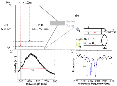
This review focuses on sensors based on diamond and especially one of the most prominent point defects in diamond, the nitrogen vacancy (NV) color center. This defect consists of a nitrogen atom replacing a carbon atom and a neighboring lattice vacancy Davies and Hamer (1976). Figure 1 summarizes its basic properties. NV centers, in general, provide long-term photo-stable fluorescence. Their bright emission with high luminescence efficiency Radko et al. (2016) lies in the red and near-infrared spectral range and spans about 100 nm. NV color centers form emitting electric dipoles Alegre et al. (2007). Their emission is bright enough to allow for a straightforward detection of individual, isolated centers in a confocal fluorescence microscope. Thus, NV centers have been investigated as solid-state sources of single photons Kurtsiefer et al. (2000). Single photons in turn are a valuable resource for nanoscale sensing, e.g., in scanning near-field optical microscopy as a nanoscopic light source Kühn et al. (2001). Alternatively, the dipole of the NV center can interact with other dipoles and transfer energy via optical near fields (Förster resonance energy transfer (FRET) Tisler et al. (2011, 2013)). Via this process, NV centers can reveal the presence of other dipoles.
In addition to their optical properties, NV centers provide highly-coherent, optically-readable electronic spins (see Figure 1; first observation in Gruber et al. (1997)). The NV centers’ long spin coherence times (T or T2) show that coherent superposition states of the 0 and 1 ground state spin levels retain their phase for a long time even at room temperature. Here, NV centers profit from the fact that the diamond lattice naturally features a low magnetic noise. Thus, it protects these superposition states from decoherence: the most abundant carbon isotope does not have a nuclear spin. Additionally, the concentration of paramagnetic isotopes (1.1%) can be reduced by isotopically pure diamond synthesis Balasubramanian et al. (2009). In such an isotopically-engineered diamond, T2 can be as high as 1.8 ms. The NV center’s T2 is a valuable sensing resource: its decrease, for example, directly reveals the presence of magnetic molecules on the diamond surface Ermakova et al. (2013). The use of spin coherence as a sensing resource opens up novel sensing schemes with potentially enhanced sensitivity compared to classical techniques. These novel approaches are typically summarized under the term of quantum sensing (for a recent review, see, e.g., Degen et al. (2016)). However, sensing approaches that rely on the direct measurement of spin resonances (optically-detected magnetic resonance (ODMR); for an explanation, see Figure 1) and their shift in magnetic fields (Figure 1) also profit from highly-coherent NV centers: the NV’s sensitivity to static magnetic fields is given by Rondin et al. (2014):
| (1) |
where is the ODMR linewidth and is the detected photon rate from the NV center. is the fluorescence contrast in ODMR. The latter is an intrinsic property of NV centers and can hardly be modified as it is determined by the internal dynamics. is fundamentally limited by the inverse of the coherence time T and thus connects the sensitivity to the coherence properties.
Note that Equation (1) refers to non-resonant spin read-out, typically using green laser light to excite the NV center. This read-out scheme is feasible at room temperature and thus advantageous for sensing. At cryogenic temperature, resonantly-addressing spin-selective transitions within the ZPL enables single-shot read-out of the electronic spin state of NV centers Robledo et al. (2011).
The carbon lattice of diamond itself provides only a weak source of decoherence. However, paramagnetic impurities (e.g., nitrogen in its substitutional form) and spins on the diamond surface can significantly reduce the coherence time of NV centers Luan et al. (2015). Reduced coherence times render NV centers less sensitive for magnetic fields, as discernible from Equation (1). Consequently, it is vital to control this loss of coherence to use NV centers as highly-sensitive sensors for fields outside the diamond crystal.
In essence, realizing an optimal NV sensor narrows to three main aspects:
-
•
It is mandatory to reliably create stable NV centers with a controlled density buried less than 10 nm below diamond surfaces (shallow NV centers). These NV centers need to retain spin coherence for optimal sensitivity.
-
•
ODMR and optical sensing schemes demand efficient collection of fluorescence light and high photon rates from single centers. This in turn demands the incorporation of color centers into nanophotonic structures.
-
•
To realize a sensor that probes the sample surface and to realize controlled positioning of the NV sensor requires realizing a tip-like sensor and scanning probe sensing schemes.
This review is structured according to these main aspects. In Section 2, we summarize recent progress in creating and optimizing shallow NV centers. In Section 3, we turn to the photonic nanostructures for sensing and their fabrication. In Section 4, we illustrate scanning probe-based approaches, as well as recent advances in NV-based sensing.
2 Shallow NV Centers for Sensing
2.1 Creation Methods and Creation Yield
NVs with a controlled distance to diamond surfaces have been created using two approaches, namely ion implantation and -doping. We discuss both in the following:
-
•
Ion implantation: This approach relies on the commercial availability of chemical vapor deposition (CVD) diamond with low nitrogen (N) content (< 5 ppb substitutional N) and an almost negligible density of in situ-created, native NV centers (Ryan et al. (2010), element six, electronic grade diamond). This diamond is irradiated with N ions at energies typically between 4 and 8 keV. These implantation energies correspond to mean implantation depths between 7 nm and 12 nm, as calculated by Monte Carlo simulations Ziegler et al. (2010). Coherence times T2 of NVs created deep (> 50 nm) inside this material by N implantation reach T2 200 s comparable to in situ-created NV centers Wang et al. (2016). Such T2 times indicate the high purity of the material, whereas in diamonds with 100 ppm N, T2 generally reduces to about 1 s Rondin et al. (2014). After the implantation, high temperature annealing repairs crystal damage, mobilizes vacancies via diffusion and forms NV complexes via N impurities capturing vacancies. In contrast, impurities like, for example, N are not expected to diffuse at these temperatures Ofori-Okai et al. (2012). Two approaches are reported: annealing in vacuum at pressures below mbar Appel et al. (2016); Wang et al. (2016); Ofori-Okai et al. (2012), where a high vacuum is needed to avoid etching of the surface Antonov et al. (2014). Alternatively, annealing in forming gas (4% H2 in Ar) is used (e.g., Orwa et al. (2011); Santori et al. (2009)). The conversion efficiency from implanted N to NV (mostly NV-) is called yield. It amounts to typically only for an implantation energy of 5 keV (depth 8 nm) Pezzagna et al. (2010); Appel et al. (2016). For micrometer-deep implanted NVs ( MeV), the yield increases to Pezzagna et al. (2010). For shallow NVs, vacancies are partially captured by the diamond surface Antonov et al. (2014). Furthermore, higher energy implantation increases the number of vacancies produced Pezzagna et al. (2010). Very recent studies, however, indicate that increasing the number of vacancies by co-implanting, e.g., carbon, does not increase the NV yield for shallow implantation Fávaro de Oliveira et al. (2016).
-
•
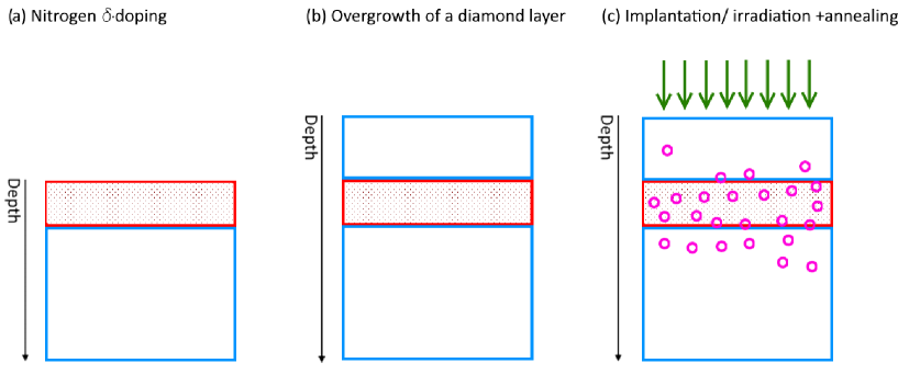
The -doping method for creating shallow NVs consists of the following steps; see Figure 2:
-
–
An N-doped, several nm-thick layer, the -doped layer Ohno et al. (2012); Osterkamp et al. (2015), is created in situ by the controlled introduction of N2 gas during slow, plasma-enhanced CVD growth of single-crystal diamond (growth rate 0.1 nm/min; Figure 2a). Changing the N2 flow tunes the resulting N densities. In order to decrease the magnetic noise, diamond growth can be performed using isotopically-purified 12CH4 as the carbon source Ohno et al. (2012, 2014); McLellan et al. (2016). Very recently, overgrowth of a nitrogen-terminated diamond surface has been employed for -doping Chandran et al. (2016).
-
–
Vacancies are created ex situ by implanting helium ions Favaro de Oliveira et al. (2016); Kleinsasser et al. (2016), carbon ions Ohno et al. (2014) or irradiating with electrons Ohno et al. (2012); McLellan et al. (2016). A subsequent annealing at high temperature causes vacancy diffusion and creates NV centers (Figure 2c). Varying the thickness of an undoped diamond layer, overgrown before the implantation step, allows controlling the depth of the NV layer (Figure 2b). The vacancy profile depends on the species used: for electron irradiation, it is flat and extends throughout the grown film and substrate Ohno et al. (2014). In contrast, implanted carbon ions are localized in the lattice. A shallow layer ( 5 nm) of implanted 12C ions has been used as the source of vacancies for a deeper ( 50 nm) -doped layer Ohno et al. (2014), taking advantage of annealing-induced diffusion. With this method, it is possible to increase the NV density in the -doped layer by increasing the 12C dose without activating NV centers in the substrate. An alternative method, applied to low energy helium implantation, consists of growing a thicker N-doped layer ( nm) and adding a last etching step to create NV centers near the surface Favaro de Oliveira et al. (2016).
NV yields reached values of Favaro de Oliveira et al. (2016) and McLellan et al. (2016), however, remaining quite low () in Ohno et al. (2014). As discussed below, often, -doping enhances the coherence times of shallow NVs compared to N implantation. Moreover, it potentially localizes NV centers in a more defined depth.
-
–
2.2 Photochromism, Quantum Efficiencies and Coherence Time
NV centers exist in two luminescent charge states: negative (NV-) and neutral (NV0) Mita (1996); only NV- exhibits ODMR. To create an NV-, an electron has to be captured by the NV center. The NV- population never exceeds – (excitation wavelength 450–610 nm) Aslam et al. (2013); Chen et al. (2013); Beha et al. (2012), due to photo-induced ionization Beha et al. (2012). In the band from 450–575 nm, NV- and NV0 absorb light. Consequently, the loop of NV- excitation-ionization and NV0 excitation-recombination is closed, and the NV cycles between both charge states. The NV- steady state population is maximized for optical excitation in the band 510–540 nm Aslam et al. (2013). Besides this photochromism, the NV charge state is directly influenced by the Fermi level position in diamond. For shallow NVs, the Fermi level position closely relates to the electron affinity of the surface (see Section 2.3).
An important characteristic for light-emitting systems is their quantum efficiency (QE). It is defined as , where , are the radiative and non-radiative decay rate of the NV center, respectively. A higher QE, in general, leads to brighter emission from the centers. For shallow NVs, QE can be as high as () for a depth of 4.1 nm (8 nm), respectively Radko et al. (2016). The work in Radko et al. (2016) estimates QE > 96% in bulk diamond. This result implies decreased QE for shallow NVs, which was attributed to non-radiative decays induced by surface strain. Generally, careful control of strain and crystalline quality seems necessary to obtain high QE: QE in the range of only – was found in ion-damaged diamond (H-implantation, fluence cm-2 corresponding to an estimated induced vacancy density ppm, Gatto Monticone et al. (2013)). NV centers in 25-nm nanodiamonds even may show QE < 20% Mohtashami and Koenderink (2013).
Generally, shallowly-implanted NV centers show reduced T2 together with broadened ODMR lines Ofori-Okai et al. (2012); Romach et al. (2015); Appel et al. (2016); Maletinsky et al. (2012). Table 1 illustrates this reduction in comparison to deep, native centers. Degraded coherence properties are related to noise created by the proximity to the surface. The work in Romach et al. (2015) presents a spectroscopic analysis of the noise (N dose 108 cm-2). High-frequency noise arises due to surface-modified phonons and low frequency noise due to the surface electronic spin bath. For ion doses of 1011 cm-2, noise produced by implanted defects close to NV centers adds to surface-related noise. Indeed, N bombardment introduces N impurities and vacancy complexes that act as paramagnetic centers, degrading the coherence time of NV centers Yamamoto et al. (2013); de Oliveira et al. (2017).
| Photocounts | T2 (s) | Linewidth (MHz) | |
|---|---|---|---|
| Very Shallow NV- (2.1 nm) | 2 | ||
| Shallow NV- (7.7 nm) | 1.2 | ||
| Native NV- (6 m) | 1 |
2.3 Methods to Improve Stability and Photoluminescence
The work in Santori et al. (2009) shows that the NV- population is decreased at depths up to 200 nm compared to bulk. This effect is attributed to the presence of an electronic depletion layer at the etched diamond surface. In this depletion region, N donors cannot donate an electron to the NV center because they are ionized. Stabilizing the NV- state close to the surface involves controlling the Fermi level in diamond Fu et al. (2010); Hauf et al. (2011); Doi et al. (2014, 2016). The Fermi level, and consequently the NV- population, can be controlled via chemical functionalization of the surface Fu et al. (2010); Hauf et al. (2011); Shanley et al. (2014); Cui and Hu (2013) (see Figure 3a,b) by applying an electrolyte gate voltage Grotz et al. (2012) (see Figure 3c) using in-plane gate nanostructures Hauf et al. (2014) or via doping the diamond Doi et al. (2016).
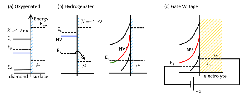
First, we consider the decrease in the NV- population of shallow NV centers close to a hydrogen (H)-terminated surface compared to an oxygenated surface Hauf et al. (2011); Fu et al. (2010). For H-terminated diamond, the conduction and valence bands shift upwards due to the negative electron affinity of the surface. The energy of the valence band maximum EV is higher than the chemical potential of the electronic states created by adsorbed water. Electrons migrate to the adsorbate layer. In equilibrium, the diamond bands bend upwards; a 2D hole gas is created; and the NV- charge state is depleted Hauf et al. (2011). Thus, H-termination is not useful to stabilize NV-.
In contrast, fluorine (F)-terminated surfaces will lead to a downward bending of the diamond bands due to the large electron affinity of F Rietwyk et al. (2013). In this case, the NV- population increases compared to H-terminated diamond Shanley et al. (2014) and also to oxygenated diamond Cui and Hu (2013). However, it should be noted that so far, coherence measurements of shallow NV centers close to F-terminated surfaces are missing.
For H-terminated diamond, electrolytic gate electrodes can directly control the Fermi level Grotz et al. (2012) (see Figure 3c). An increase in the NV- ensemble population was observed for high implantation dose and positive gate voltage. Unfortunately, no single NV charge switching was observed, due to the high gate voltage needed for charge-state conversion at low implantation dose. On the other hand, this result was achieved in Hauf et al. (2014) by applying an electric field using in-plane nanostructures. The gate-voltage was applied to a structure formed by H-terminated areas and an O-terminated line, resulting in an offset between the Fermi level in the H-terminated areas on both sides of the line. In this way, switching the charge state of a single NV center from NV0 to NV- was established.
Deterministic electrical control of the charge state of a single NV center has been achieved using a p-i-n diode Doi et al. (2014). The NV center is positioned in the intrinsic region of the diode, and a current of holes is induced from the p-region. However, this technique converts NV centers to NV0. Using in plane Al-Schottky diodes, based on H-terminated diamond, charge state switching of single NV centers (NV+ to NV0 to NV-) has been obtained Schreyvogel et al. (2015). Implementing diode structures in scanning probe sensing seems, however, highly challenging.
Another way to change the Fermi level of diamond is by boron or phosphorus (P) doping Doi et al. (2016); Groot-Berning et al. (2014). In particular, P impurities donate an electron to NV0, due to the fact that the P activation energy is low ( eV) compared to NV acceptor states ( eV). In this way, a five-fold increase in luminescence and a pure NV- state was observed for a single NV Doi et al. (2016) and a P doping cm-3. It should be noted that this single NV had a short coherence time T2 = (19.77 0.27) s, and the depth of the NV center in this case was not reported.
2.4 Methods to Improve T2
In this section, we discuss how N -doping Ohno et al. (2012); Chandran et al. (2016) and ion implantation Huang et al. (2013); Favaro de Oliveira et al. (2016); Naydenov et al. (2010) or electron irradiation McLellan et al. (2016) can lead to improved spin coherence. Figure 4 summarizes recently obtained T2 values for different methods and works. As discussed above, implanted defects are sources of noise. Implanted defects can be of two types:
The formation of vacancy complexes during annealing is inhibited by Coulomb repulsion, if their charge state is changed from neutral to positive de Oliveira et al. (2017). Vacancy charging is accomplished in a p-i junction by implanting N in the junction’s space charge layer. A two-fold increase in yield and ten-fold increase in T2 for very shallow NVs has been reported (T2 = 30 s, NV depth d = 3 nm).
Noise from implantation-induced impurities and crystal defects can be reduced using -doping and ex situ creation of vacancies (see Section 2.1). To be used in scanning probe sensing, NV centers should have a depth below 10 nm. As mentioned before, this can be achieved by tuning the dimension of the cap layer Ohno et al. (2012) or adding a last etching step Favaro de Oliveira et al. (2016). In this depth range, the maximum reached T2 is 200 s obtained when irradiating an isotopically-purified sample with electrons Ohno et al. (2012). In this case, however, the NV density was too low for applications requiring the fabrication of single-crystal scanning probes, as discussed below.
We remark that NV areal densities around cm-2 are typically necessary for single crystal scanning probes: this corresponds to one NV center in a circular area with a diameter of 200 nm and thus to a single NV in typical nanostructures used for sensing (see Section 3). In Ohno et al. (2012), the -doped layer has an N concentration of cm-3, considering a layer thickness of 2 nm; this results in an areal density of N of cm-2, so in order to have an acceptable NV areal density, one should have a very high yield, around . A similar concentration of N ( cm-3) is reported in Ohno et al. (2014), leading to a low NV area density ( cm-2). A slightly too low NV density is reported in McLellan et al. (2016) cm-2 and in Favaro de Oliveira et al. (2016) cm-2. It is worth noticing that an N volume concentration of cm-3 is reported in Chandran et al. (2016); this would result in an NV density of cm-2, considering a thickness layer of 2 nm and a yield of . In contrast, the N implantation method described in de Oliveira et al. (2017) seems more promising from this point of view: tuning the fluence of implanted N from cm-2– cm-2 (E = 5 keV) allows accessing the optimal densities of shallow NV centers.
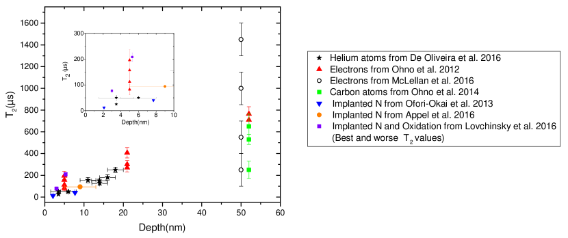
We underline that till now, -doping has not been applied in the manufacturing of diamond probes for nanosensing. This is probably due to the fact that -doping involves the realization of sophisticated CVD methods. In contrast, creating single NVs by ion implantation can be achieved using commercial diamond material and implantation facilities.
Finally, we remark that surface oxidation has been used recently to improve T2 Lovchinsky et al. (2016). Wet oxidative chemistry and sample annealing at 465 ∘C in a dry oxygen atmosphere increased T2 by an order of magnitude (max. T s for a single NV, depth nm, T s observed for 6 NVs). Recent work Yamano et al. (2017), however, was not able to reproduce these results for shallower NVs: in Yamano et al. (2017), a similar oxidation procedure resulted in T2 s for calculated depths of nm.
3 Nanostructures for Photonics and Scanning Probe Operation
NV centers close to the surface of bulk, single-crystal diamond are, on the one hand, advantageous as they reside in high-quality, high-purity, potentially low-stress diamond material mostly synthesized by the CVD method Balmer et al. (2009). On the other hand, these NV centers do not fulfill all prerequisites for nanoscale sensing: first, positioning an NV created in a macroscopic diamond crystal within nanometer distance from a sample is hardly feasible. In principle, attaching the ‘sample’, e.g., the substance under investigation, to a scanning probe tip while keeping the NV center stationary can circumvent this issue. However, this limits the technique to microscopic samples, e.g., specific molecules or ions (e.g., Pelliccione et al. (2014)) for which attachment to a nano-sized tip is feasible.
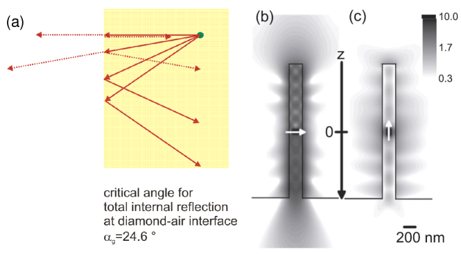
Additionally, even for an optimal dipole orientation, a typical air microscope objective (NA 0.8 Neu et al. (2014)) collects only about 5% of the fluorescence from an NV center in bulk diamond: as diamond exhibits a high refractive index of 2.4 for visible light Zaitsev (2001), only light incident at angles < 24.6∘ (partially) leaves the diamond as illustrated in Figure 5a. Other light rays are lost due to total internal reflection. Additionally, the dipolar emission from color centers is typically directed towards the optically-dense medium. Thus, in our case, emission is directed towards the bulk diamond, additionally hindering fluorescence detection Lukosz and Kunz (1977); Hausmann et al. (2010). Consequently, coupling to nanophotonic structures is mandatory to enhance the photon rates from individual color center sensors in single-crystal diamond. Alternatively, attaching nanodiamonds (NDs) containing NV centers to a scanning probe tip provides a scannable NV platform (e.g., Tetienne et al. (2015); Tisler et al. (2013)). However, NDs show non-ideal material properties, typically due to excess nitrogen or crystal strain resulting from milling of the material Santori et al. (2010). Thus, incorporated color centers may suffer from short coherence time, strong inhomogeneous line spreads and reduced stability Bradac et al. (2010). In this review, we thus focus on single-crystal diamond-based sensing techniques.
Scanning probe sensing demands nanophotonic structures with several properties:
-
•
Broadband operation: Section 1 and Figure 1c illustrate the 100 nm-broad room temperature emission spectrum of NV centers. Room temperature spin read-out under non-resonant excitation is most efficient if the integral emission is detected. Thus, the photonic structure should allow for efficient fluorescence detection from the complete NV emission spectrum.
-
•
Tip-like geometry and suitability for NV centers close to surfaces: a tip-like geometry ensures close proximity of the scannable NV center to the sample even in the presence of alignment uncertainties. The photonic structure needs to be functional for NV centers very close to diamond surfaces.
-
•
Attachment to the feedback system: the nanostructure has to be attached to a force sensor, i.e., a tuning fork or a cantilever. A miniaturized structure is needed, thus avoiding strong shifting of the resonance frequency due to the additional mass or severe damping of the oscillating system.
Considering the first criterion, resonant photonic structures, like, e.g., photonic crystal cavities Faraon et al. (2012), which selectively enhance a specific transition within the emission spectrum, are not fully suitable for sensing applications under ambient conditions. For quantum information, in contrast, these systems are promising as they potentially form a coherent interface between spins and photons in quantum networks Li et al. (2015). In our case, waveguide-like structures that channel the NV’s broad emission into certain spatial modes and direct the light towards the collection optics (nanopillars; see Figure 5b) seem more suitable mainly due to their broadband operation. Certain waveguide-based structures, i.e., dielectric antennas Lee et al. (2011), have been found to enable potentially near unity collection efficiency for NV fluorescence Riedel et al. (2014). However, they consist of planar multilayer structures and are thus not optimized for scanning probe sensing. In contrast, they might be very suitable for approaches where a diamond chip is used for sensing (wide field approaches, lower spatial resolution, e.g., Le Sage et al. (2013)). Taking into account the first two criteria, also solid immersion lenses, where color centers are buried inside diamond half spheres, are not suitable Marseglia et al. (2011). In this review, we focus on the nanostructure types suitable for scanning probe sensing. For more complete recent reviews of diamond nanophotonics in the context of quantum information, see Hausmann et al. (2012); Beha et al. (2012); Aharonovich and Neu (2014); Schroder et al. (2016).
In essence, photonic nanostructures suitable for scanning probe sensing consist of a roughly tip-shaped nanophotonic structure on a thin (typically < 1 m) diamond mounting structure, as shown in Figure 6a. First, operational sensors have been presented in 2012 Maletinsky et al. (2012). The work in Appel et al. (2016); Kleinlein et al. (2016) presents more recent nanofabrication approaches. In a further very recent approach, mounting structures holding an array of pillars are used. Consequently, several NV centers are usable, and vector magnetometry might be feasible Pelliccione et al. (2016). However, this approach introduces the risk that a pillar that is not in direct contact with the sample is used and, thus, an unwanted stand-off distance strongly reduces the resolution.
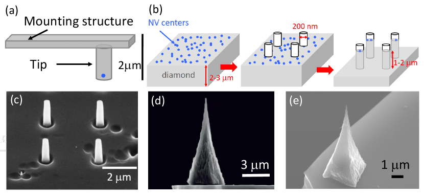
We start by addressing how large-area, thin, single-crystal diamond membranes can be formed. High-purity, CVD diamond with < 5 ppb substitutional nitrogen and an intrinsically very low density of NV centers is commercially available (see Section 2.1). Starting from this material, thin, single-crystal diamond membranes can be formed by thinning down diamond plates obtained by polishing (typically several tens of m thick). To thin the plates down, reactive-ion etching with different reactive gases in the plasma has been used among them chlorine and oxygen-based recipes Maletinsky et al. (2012); Appel et al. (2016), fully-chlorine-based chemistry Tao et al. (2014), oxygen/fluorine-based chemistry Kleinlein et al. (2016); Jung et al. (2016) and fully-fluorine-based chemistry Ali Momenzadeh et al. (2016). For all of these approaches except in Kleinlein et al. (2016), argon is added to the plasma to introduce physical etching (sputter etching) to the process. Alternatively, membranes can be created by damaging a buried layer of diamond via ion implantation. When this layer is graphitized upon annealing, it can be chemically etched, and membranes are lifted-off. However, due to strong ion damage, this material is not directly usable and has to be overgrown with a pristine layer of CVD diamond, adding technological complexity to the process Piracha et al. (2016). We note that it is not possible to obtain thin, low-stress, single-crystal membranes directly via growth on a non-diamond substrate that might allow for wet-chemical etching of the substrate: for all diamond heteroepitaxy, the starting phase of the growth is highly defective, and forming high-quality, thin membranes includes removing this initial growth areas Riedrich-Möller et al. (2012). Reliable, large-area fabricating of single-crystal membranes is essential for high-yield fabrication of scanning probe devices and potential future up-scaling of the technology.
The nanostructure forming the tip is either almost cylindrical (termed nanopillar Babinec et al. (2010); Hausmann et al. (2010, 2011); Neu et al. (2014); Appel et al. (2016)), pyramidal Nelz et al. (2016) or features a truncated cone shape with a taper angle Momenzadeh et al. (2015); Hausmann et al. (2010). The work in Momenzadeh et al. (2015) demonstrated that tapering the pillar enhances fluorescence rates from single NVs. Lithographically-defined etch masks are used to create the pillars, as illustrated in Figure 6b. These masks undergo faceting and erosion Jiang et al. (2016), thus limiting the pillar length and influencing its shape. For an electron microscopy image of diamond nanopillars, see Figure 6c. Mask erosion is especially critical, as a high-density plasma (mostly oxygen and argon) is needed to enable highly-anisotropic etching of diamond. For the coupling to the nanostructure’s photonic modes, not only the placement of the NV center is essential, but also the orientation of the NV’s electric dipoles. As indicated in Figure 5b, placing the NV’s dipoles perpendicularly to the pillar axis is the most advantageous configuration. This situation can be reached in <111>-oriented diamond. Here, NV centers created during CVD growth preferentially align in the growth direction, with their dipoles in the plane perpendicular to that direction Lesik et al. (2014); Michl et al. (2014); Fukui et al. (2014). However, CVD growth in the <111> crystal direction is challenging Tallaire et al. (2014) and still leads to a material with lower quality than the standard <100> growth. In <100> diamond, NV centers align along all four equivalent <111> directions and have an oblique angle of 54.7∘ with the pillar axis. As an alternative, CVD growth in the <113> direction has been investigated Lesik et al. (2015). In this material, 73% of NVs form an angle of 29.5∘ with the potential pillar axis and thus bring their dipoles closer to the ideal orientation. The work in Neu et al. (2014) demonstrates pillars fabricated into <111>-oriented material. However, so far, optimized crystal orientations have not been used for scanning probe sensing.
To manufacture nanophotonic structures, two fundamentally different approaches exist: first, the structures can be sculpted from bulk diamond material (top-down approach) as discussed above Babinec et al. (2010); Hausmann et al. (2010); Neu et al. (2014); Appel et al. (2016); Jiang et al. (2016). In contrast, nanostructures might also be created directly during (CVD) synthesis of diamond (bottom up approach Nelz et al. (2016); Aharonovich et al. (2013); Zhang and Hu (2016)). Pyramidal nanostructures formed via bottom-up approaches (see Figure 6d,e) also have advantageous photonic properties Nelz et al. (2016). However, they currently show high levels of color center incorporation during growth. This results from growth on non-diamond materials or incorporation of impurities from masks used in the growth. Consequently, these structures are not usable for sensing with single color centers so far. In top-down approaches, plasma-based etching forms the nano-structures. The work in de Oliveira et al. (2015) shows that a plasma can damage the diamond surface and reduce NV coherence. From this point of view, bottom-up approaches are appealing as they offer the opportunity to avoid plasma etching of diamond.
As discussed in Section 2, shallow NV creation is a crucial step towards functional sensing devices. So far, NVs in nanopillars have been created by ion implantation Maletinsky et al. (2012); Hausmann et al. (2011); Appel et al. (2016); Momenzadeh et al. (2015) followed by structuring the nanopillars via lithography and etching (see Figure 6b). Alternatively, NV centers created during growth, but at non-defined depth, were used Babinec et al. (2010); Neu et al. (2014). Thus, the latter pillars are not suitable for scanning probe sensing. A promising alternative approach is spatially localized ion implantation into high-purity nanostructures. Three different approaches have been presented: the first uses focused nitrogen ion beams for localized implantation Lesik et al. (2013). In the second approach, a pierced AFM tip is used as an implantation aperture Meijer et al. (2008). In the third approach, single ion traps are planned to be used as deterministic sources of implanted ions Jacob et al. (2016). Also in the context of -doping, three-dimensional localization of NV centers has been reported: Ohno et al. (2014) uses a mask with nanometric apertures for single NV creation in a -doped layer. For the smallest aperture of () nm, single NVs were created in of the apertures. In McLellan et al. (2016), a transmission electron microscope is used for irradiation, achieving sub-micron accuracy in lateral positioning.
We point out that in parallel to the efforts in nanophotonics, recently electrical read-out of the NV spin state has been proposed alternatively to the challenging optical read-out: NV centers are more likely to undergo multi-photon photo-ionization as long as they are not being shelved to the singlet states. Thus, an NV center in the spin state is more likely to be ionized and leads to a higher photo-current. Demonstrations include continuous Bourgeois et al. (2015), as well as pulsed detection Hrubesch et al. (2017). Whereas the read-out contrast can approach 20%, demonstrations of single NV read-out are still pending.
4 Recent Advances in NV Sensing
In this section, we review selected recent advances in sensing with single NV centers. In Section 4.1, we summarize recent steps towards scanning near-field optical microscopy (SNOM) with a single NV center. In Section 4.2, we present recent results using the magnetic sensing capabilities of NV centers (atomic size sensor, high sensitivity, low-invasiveness) to study physical phenomena at low temperature and/or few atoms level.
4.1 Near-Field Microscopy with NV Centers
In recent years, the highly-photostable emission of individual NV centers has triggered several efforts to realize near-field sensing based on NV centers Tisler et al. (2011, 2013); Sekatskii et al. (2015); Drezet et al. (2015). In general, near-field-based imaging, where a sample is illuminated by the near-field of a light source, allows a higher resolution than far field-based techniques and is able to beat the Abb limit of resolution.
Single NV centers were used as nano-sized light-source that is brought within < 100 nm of the sample in a SNOM setup Kühn et al. (2001); Cuche et al. (2009); Drezet et al. (2015). A nanodiamond (ND) attached to the end of a SNOM tip achieved a resolution of around 50 nm when imaging metallic nanostructures, thus beating the Abb limit of resolution (see Figure 7). The resolution was limited by the vertical NV-to-sample distance, which is constrained by the ND size and by the fact that the ND was not put in contact with the sample to avoid too strong friction forces at the tip apex.
Förster resonance energy transfer (FRET) was first described as non-radiative energy transfer between a pair of single molecules (dipoles) in close proximity Förster (1948); Dexter (1953). To enable FRET, the emission band of the donor molecule has to overlap with the absorption band of the acceptor molecule, allowing energy transfer from the donor to the acceptor molecule. The transfer efficiency reaches 50% for a characteristic distance, the so-called Förster distance , and drops with the inverse sixth power of the distance. NV centers in a FRET pair with a fluorescent dye have shown = 5.6 nm Mohan et al. (2010). Thus, this effect promises truly nanoscale resolution in near-field-based imaging.
In recent experiments, an ND placed close to the apex of a commercial AFM tip was scanned close to a surface covered with graphene flakes Tisler et al. (2013). The NV center and the graphene flake form a FRET pair. A Förster distance of 15 nm was found. Sekatskii and co-workers Sekatskii et al. (2015) reported on unsuccessful experiments on FRET transfer between a scanning NV and a dye molecule, despite previous demonstration of FRET to dye molecules covalently bonded to NDs Tisler et al. (2011). This finding might relate to a varying quantum efficiency (QE) for NV centers in NDs Mohtashami and Koenderink (2013), the need for accurate control of the ND surface (graphite layers), as well as to large stand-off distances when attaching an ND to a scanning probe tip. These issues may be addressable in the future using scanning probe devices sculpted out of single-crystal diamond Appel et al. (2016); Maletinsky et al. (2012). So far, no experiments on near-field sensing based on single-crystal scanning probes have been reported.
Finally, we mention that super-resolution images of NV centers in bulk diamond were recorded using stimulated emission depletion microscopy Rittweger et al. (2009), ground state depletion microscopy Han et al. (2010), stochastic optical reconstruction microscopy Pfender et al. (2014) and by sampling second- and third- order photon correlation function Monticone et al. (2014). These techniques beat the Abb resolution limit without the need for near-field imaging.
4.2 Recent Applications of Single NV Sensing
The implementation of scanning NV-based microscopy at cryogenic temperatures forms a recent milestone: in a preliminary realization, cryogenic operation was achieved with a single NV center in bulk material and a scanning magnetic tip Schaefer-Nolte et al. (2014). More recently, versatile approaches with NV centers in single crystal scanning probes have been presented Pelliccione et al. (2016); Thiel et al. (2016). This technology significantly broadens the range of samples for which NV magnetometry can be applied: solid materials present unique phenomena that only occur at cryogenic temperatures such as superconductivity. An ideal superconductor is supposed to expel all magnetic fields (Meissner effect). However, real superconductors present points at which magnetic fields penetrate and magnetic vortices form. NV nano-magnetometry was applied for a high-resolution, low-invasive imaging of superconducting vortices (6 K, Pelliccione et al. (2016), 4.2 K Thiel et al. (2016)). To achieve cryogenic operation, the NV microscope is enclosed in a liquid 4He cryostat with optical access. Particular care was taken to avoid heating by microwave (MW) and laser excitation. Superconducting vortices were imaged with a resolution below 100 nm with magnetic field sensitivity of 30 THz1/2 Pelliccione et al. (2016) and 11.9 THz1/2 Thiel et al. (2016), allowing in Thiel et al. (2016) to verify vortex models beyond the monopole approximation.
Very recently, NV microscopy imaged nanoscale ferrimagnetic domains in antiferromagnetic random access memories Kosub et al. (2017). We underline that part of these measurements were performed in zero field cooling (ZFC), taking advantage of low-invasive sensing using NV centers.
As discussed above, NV microscopy is often employed to sense static magnetic fields with nanoscale spatial resolution. However, NV centers are also sensitive to magnetic fields oscillating at GHz frequencies: single-crystal NV scanning probes imaged magnetic fields generated by MW currents with nanoscale resolution and sensitivity of a few nAHz1/2 Appel et al. (2015). The basic idea is to tune an NV spin resonance to the investigated MW frequency using a static magnetic field. The induced coherent spin oscillation frequency (Rabi frequency) then maps the magnetic field amplitude.
Single NV centers also form atomic-sized probes for nuclear magnetic resonance (NMR) signals Wrachtrup and Finkler (2016); Mamin et al. (2013); Staudacher et al. (2013). The NV spin state is sensitive to the stochastic transverse magnetization at the Larmor frequency of the investigated ensemble of nuclei. Using suitable pulse sequences, it is possible to filter NMR signals and recover NMR spectra. Using NV probes, NMR investigations of small ensembles of nuclei are feasible. In contrast, conventional NMR spectroscopy is limited to macroscopic, thermally-polarized ensembles in high fields. Recent work presents NMR studies of a single protein Lovchinsky et al. (2016) and of atomically-thin hexagonal boron nitride (h-BN) layers Lovchinsky et al. (2017). 2H and 13C NMR spectra of ubiquitin proteins were measured Lovchinsky et al. (2016), paving the way for experimental studies of biological systems at the single-molecule level. Conventional nuclear quadrupole resonance (NQR) Das and Hahn (1958) spectroscopy yields important information on chemical properties of macroscopic samples. However, it suffers from poor sensitivity due to low thermal polarization. This issue can be overcome using single NV centers that are sensitive to stochastic nuclear magnetization. The stochastic polarization is proportional to , where is the number of nuclei, but does not depend on the applied field. Single NV NQR was applied to study thin h-BN flakes, verifying a correlation between the number of atomic layers and a shift in NQR spectra Lovchinsky et al. (2017).
NMR imaging has already been partially combined with scanning NV microscopy, in the sense that samples on a tip were scanned above a stationary NV. This configuration has been used for magnetic resonance imaging of 1H nuclei with a spatial resolution of 12 nm Rugar et al. (2015). 19F nuclei were imaged in a calibration grating Häberle et al. (2015); widths of nm were resolved Häberle et al. (2015). To the best of our knowledge, to date, there are no reports on the use of single-crystal diamond scanning probes for NMR imaging. However, this fact does not represent a general limitation. It most probably relates to the fact that because of challenging nanofabrication procedures, only a few research groups have access to single-crystal scanning probes so far.
5 Conclusions
We have summarized recent achievements and the basics of NV center-based sensing. The fabrication of suitable photonic nanostructures that allow scanning probe sensing and high photon rates from single centers, as well as the creation of NV color centers close to the diamond surface are still challenging subjects of research. To date, many recent advances like the creation of NV centers via -doping methods, optimized surface treatments and doping of diamond, as well as diamond crystals with optimized orientation have not yet been used in the challenging fabrication of single-crystal diamond scanning probes. Thus, enhanced sensitivities and resolution in NV-based imaging are feasible in the future, given that the recent advances in material sciences are fully transferred to the sensor fabrication. As discussed in this review, many approaches to optimal, shallow NV centers are investigated. The results considering creation yield and NV properties are not always fully consistent, illustrating the complexity of the field. Moreover, the field could tremendously profit from simplified procedures to upscale the fabrication of optimized sensing nanostructures.
Acknowledgements.
The authors acknowledge funding via a NanoMatFutur grant of the German Ministry of Education and Research. Elke Neu acknowledges funding via a PostDoc fellowship of the Daimler and Benz foundation. \authorcontributionsEttore Bernardi and Elke Neu wrote the manuscript. Selda Sonusen and Richard Nelz performed the experiments and contributed experimental data (NV spectroscopy, ODMR, nanowires). All authors discussed and commented on the manuscript. \conflictsofinterestThe authors declare no conflict of interest.References
- Dresselhaus (2016) Dresselhaus, M.S. A revolution of nanoscale dimensions. Nat. Rev. Mater. 2016, 1, 15017.
- Wilhelm et al. (2016) Wilhelm, S.; Tavares, A.J.; Dai, Q.; Ohta, S.; Audet, J.; Dvorak, H.F.; Chan, W.C. Analysis of nanoparticle delivery to tumours. Nat. Rev. Mater. 2016, 1, 16014.
- Wagner et al. (2017) Wagner, T.; Strasberg, P.; Bayer, J.C.; Rugeramigabo, E.P.; Brandes, T.; Haug, R.J. Strong suppression of shot noise in a feedback-controlled single-electron transistor. Nat. Nanotechnol. 2017, 12, 218–222.
- Nowodzinski et al. (2015) Nowodzinski, A.; Chipaux, M.; Toraille, L.; Jacques, V.; Roch, J.F.; Debuisschert, T. Nitrogen-Vacancy centers in diamond for current imaging at the redistributive layer level of Integrated Circuits. Microelectron. Reliab. 2015, 55, 1549–1553.
- Dolde et al. (2014) Dolde, F.; Doherty, M.W.; Michl, J.; Jakobi, I.; Naydenov, B.; Pezzagna, S.; Meijer, J.; Neumann, P.; Jelezko, F.; Manson, N.B.; et al. Nanoscale Detection of a Single Fundamental Charge in Ambient Conditions Using the NV- Center in Diamond. Phys. Rev. Lett. 2014, 112, 097603.
- Kucsko et al. (2013) Kucsko, G.; Maurer, P.; Yao, N.; Kubo, M.; Noh, H.; Lo, P.; Park, H.; Lukin, M. Nanometre-scale thermometry in a living cell. Nature 2013, 500, 54–58.
- Ali Momenzadeh et al. (2016) Ali Momenzadeh, S.; de Oliveira, F.F.; Neumann, P.; Bhaktavatsala Rao, D.D.; Denisenko, A.; Amjadi, M.; Chu, Z.; Yang, S.; Manson, N.B.; Doherty, M.W.; et al. Thin Circular Diamond Membrane with Embedded Nitrogen-Vacancy Centers for Hybrid Spin-Mechanical Quantum Systems. Phys. Rev. Appl. 2016, 6, 024026.
- Tisler et al. (2011) Tisler, J.; Reuter, R.; Lämmle, A.; Jelezko, F.; Balasubramanian, G.; Hemmer, P.R.; Reinhard, F.; Wrachtrup, J. Highly Efficient FRET from a Single Nitrogen-Vacancy Center in Nanodiamonds to a Single Organic Molecule. ACS Nano 2011, 5, 7893–7898.
- Binnig et al. (1986) Binnig, G.; Quate, C.F.; Gerber, C. Atomic Force Microscope. Phys. Rev. Lett. 1986, 56, 930–933.
- Martin and Wickramasinghe (1987) Martin, Y.; Wickramasinghe, H.K. Magnetic imaging by force microscopy with 1000 resolution. Appl. Phys. Lett. 1987, 50, 1455–1457.
- Ohnesorge and Binnig (1993) Ohnesorge, F.; Binnig, G. True Atomic Resolution by Atomic Force Microscopy Through Repulsive and Attractive Forces. Science 1993, 260, 1451–1456.
- Grinolds et al. (2013) Grinolds, M.; Hong, S.; Maletinsky, P.; Luan, L.; Lukin, M.; Walsworth, R.; Yacoby, A. Nanoscale magnetic imaging of a single electron spin under ambient conditions. Nat. Phys. 2013, 9, 2145.
- Rondin et al. (2014) Rondin, L.; Tetienne, J.P.; Hingant, T.; Roch, J.F.; Maletinsky, P.; Jacques, V. Magnetometry with nitrogen-vacancy defects in diamond. Rep. Prog. Phys. 2014, 77, 056503.
- Förster (1948) Förster, T. Zwischenmolekulare Energiewanderung und Fluoreszenz. Ann. Phys. 1948, 437, 55–75.
- Acosta and Hemmer (2013) Acosta, V.; Hemmer, P. Nitrogen-vacancy centers: Physics and applications. MRS Bull. 2013, 38, 127–130.
- Ofori-Okai et al. (2012) Ofori-Okai, B.K.; Pezzagna, S.; Chang, K.; Loretz, M.; Schirhagl, R.; Tao, Y.; Moores, B.A.; Groot-Berning, K.; Meijer, J.; Degen, C.L. Spin properties of very shallow nitrogen vacancy defects in diamond. Phys. Rev. B 2012, 86, 081406.
- Bradac et al. (2013) Bradac, C.; Gaebel, T.; Pakes, C.I.; Say, J.M.; Zvyagin, A.V.; Rabeau, J.R. Effect of the Nanodiamond Host on a Nitrogen-Vacancy Color-Centre Emission State. Small 2013, 9, 132–139.
- Zaitsev (2001) Zaitsev, A. Optical Properties of Diamond: A Data Handbook; Springer: Berlin Heidelberg, Germany, 2001.
- Aharonovich et al. (2011) Aharonovich, I.; Castelletto, S.; Simpson, D.; Su, C.; Greentree, A.; Prawer, S. Diamond-based single-photon emitters. Rep. Prog. Phys. 2011, 74, 076501.
- Kraus et al. (2014) Kraus, H.; Soltamov, V.; Fuchs, F.; Simin, D.; Sperlich, A.; Baranov, P.; Astakhov, G.; Dyakonov, V. Magnetic field and temperature sensing with atomic-scale spin defects in silicon carbide. Sci. Rep. 2014, 4, 5303.
- Manson et al. (2006) Manson, N.B.; Harrison, J.P.; Sellars, M.J. Nitrogen-vacancy center in diamond: Model of the electronic structure and associated dynamics. Phys. Rev. B 2006, 74, 104303.
- Collins et al. (1983) Collins, A.; Thomaz, M.; Jorge, M. Luminescence decay time of the 1.945 eV centre in type Ib diamond. J. Phys. C 1983, 16, 2177–2181.
- Robledo et al. (2011) Robledo, L.; Bernien, H.; van der Sar, T.; Hanson, R. Spin dynamics in the optical cycle of single nitrogen-vacancy centres in diamond. New J. Phys. 2011, 13, 025013.
- Alegre et al. (2007) Alegre, T.P.M.; Santori, C.; Medeiros-Ribeiro, G.; Beausoleil, R.G. Polarization-selective excitation of nitrogen vacancy centers in diamond. Phys. Rev. B 2007, 76, 165205.
- Appel et al. (2015) Appel, P.; Ganzhorn, M.; Neu, E.; Maletinsky, P. Nanoscale microwave imaging with a single electron spin in diamond. New J. Phys. 2015, 17, 112001.
- Dréau et al. (2011) Dréau, A.; Lesik, M.; Rondin, L.; Spinicelli, P.; Arcizet, O.; Roch, J.F.; Jacques, V. Avoiding power broadening in optically detected magnetic resonance of single NV defects for enhanced dc magnetic field sensitivity. Phys. Rev. B 2011, 84, 195204.
- Davies and Hamer (1976) Davies, G.; Hamer, M. Optical studies of the 1.945 eV vibronic band in diamond. Philos. Trans. Roy. Soc. A 1976, 348, 285.
- Radko et al. (2016) Radko, I.P.; Boll, M.; Israelsen, N.M.; Raatz, N.; Meijer, J.; Jelezko, F.; Andersen, U.L.; Huck, A. Determining the internal quantum efficiency of shallow-implanted nitrogen-vacancy defects in bulk diamond. Opt. Express 2016, 24, 27715–27725.
- Kurtsiefer et al. (2000) Kurtsiefer, C.; Mayer, S.; Zarda, P.; Weinfurter, H. Stable Solid-State Source of Single Photons. Phys. Rev. Lett. 2000, 85, 290–293.
- Kühn et al. (2001) Kühn, S.; Hettich, C.; Schmitt, C.; Poizat, J.P.; Sandoghdar, V. Diamond colour centres as a nanoscopic light source for scanning near-field optical microscopy. J. Microsc. 2001, 202, 2–6.
- Tisler et al. (2013) Tisler, J.; Oeckinghaus, T.; Stöhr, R.J.; Kolesov, R.; Reuter, R.; Reinhard, F.; Wrachtrup, J. Single defect center scanning near-field optical microscopy on graphene. Nano Lett. 2013, 13, 3152–3156.
- Gruber et al. (1997) Gruber, A.; Dräbenstedt, A.; Tietz, C.; Fleury, L.; Wrachtrup, J.; von Borczyskowski, C. Scanning confocal optical microscopy and magnetic resonance on single defect centers. Science 1997, 276, 2012–2014.
- Balasubramanian et al. (2009) Balasubramanian, G.; Neumann, P.; Twitchen, D.; Markham, M.; Kolesov, R.; Mizuochi, N.; Isoya, J.; Achard, J.; Beck, J.; Tissler, J.; et al. Ultralong spin coherence time in isotopically engineered diamond. Nat. Mater. 2009, 8, 383–387.
- Ermakova et al. (2013) Ermakova, A.; Pramanik, G.; Cai, J.M.; Algara-Siller, G.; Kaiser, U.; Weil, T.; Tzeng, Y.K.; Chang, H.C.; McGuinness, L.P.; Plenio, M.B.; et al. Detection of a Few Metallo-Protein Molecules Using Color Centers in Nanodiamonds. Nano Lett. 2013, 13, 3305–3309.
- Degen et al. (2016) Degen, C.; Reinhard, F.; Cappellaro, P. Quantum sensing. arXiv Preprint 2016, arXiv:1611.02427.
- Robledo et al. (2011) Robledo, L.; Childress, L.; Bernien, H.; Hensen, B.; Alkemade, P.F.; Hanson, R. High-fidelity projective read-out of a solid-state spin quantum register. Nature 2011, 477, 574–578.
- Luan et al. (2015) Luan, L.; Grinolds, M.S.; Hong, S.; Maletinsky, P.; Walsworth, R.L.; Yacoby, A. Decoherence imaging of spin ensembles using a scanning single-electron spin in diamond. Sci. Rep. 2015, 5, 8119.
- Ryan et al. (2010) Ryan, C.A.; Hodges, J.S.; Cory, D.G. Robust Decoupling Techniques to Extend Quantum Coherence in Diamond. Phys. Rev. Lett. 2010, 105, 200402.
- Ziegler et al. (2010) Ziegler, J.F.; Ziegler, M.D.; Biersack, J.P. SRIM—The stopping and range of ions in matter (2010). Nucl. Instrum. Methods Phys. Res. Sect. B Beam Interact. Mater. At. 2010, 268, 1818–1823.
- Wang et al. (2016) Wang, J.; Zhang, W.; Zhang, J.; You, J.; Li, Y.; Guo, G.; Feng, F.; Song, X.; Lou, L.; Zhua, W.; Wang, G. Coherence times of precise depth controlled NV centers in diamond. Nanoscale 2016, 8, 5780–5785.
- Appel et al. (2016) Appel, P.; Neu, E.; Ganzhorn, M.; Barfuss, A.; Batzer, M.; Gratz, M.; Tschöpe, A.; Maletinsky, P. Fabrication of all diamond scanning probes for nanoscale magnetometry. Rev. Sci. Instrum. 2016, 87, 063703.
- Antonov et al. (2014) Antonov, D.; Häußermann, T.; Aird, A.; Roth, J.; Trebin, H.R.; Müller, C.; McGuinness, L.; Jelezko, F.; Yamamoto, T.; Isoya, J.; et al. Statistical investigations on nitrogen-vacancy center creation. Appl. Phys. Lett. 2014, 104, 012105.
- Orwa et al. (2011) Orwa, J.O.; Santori, C.; Fu, K.M.C.; Gibson, B.; Simpson, D.; Aharonovich, I.; Stacey, A.; Cimmino, A.; Balog, P.; Markham, M.; et al. Engineering of nitrogen-vacancy color centers in high purity diamond by ion implantation and annealing. J. Appl. Phys. 2011, 109, 083530.
- Santori et al. (2009) Santori, C.; Barclay, P.E.; Fu, K.M.C.; Beausoleil, R.G. Vertical distribution of nitrogen-vacancy centers in diamond formed by ion implantation and annealing. Phys. Rev. B 2009, 79, 125313.
- Pezzagna et al. (2010) Pezzagna, S.; Naydenov, B.; Jelezko, F.; Wrachtrup, J.; Meijer, J. Creation efficiency of nitrogen-vacancy centres in diamond. New J. Phys. 2010, 12, 065017.
- Fávaro de Oliveira et al. (2016) Fávaro de Oliveira, F.; Momenzadeh, S.A.; Antonov, D.; Fedder, H.; Denisenko, A.; Wrachtrup, J. On the efficiency of combined ion implantation for the creation of near-surface nitrogen-vacancy centers in diamond. Phys. Status Solidi A 2016, 213, 2044–2050.
- Ohno et al. (2012) Ohno, K.; Heremans, F.J.; Bassett, L.C.; Myers, B.A.; Toyli, D.M.; Jayich, A.C.B.; Palmstrom, C.J.; Awschalom, D.D. Engineering shallow spins in diamond with nitrogen delta-doping. Appl. Phys. Lett. 2012, 101, 082413.
- Osterkamp et al. (2015) Osterkamp, C.; Lang, J.; Scharpf, J.; Müller, C.; McGuinness, L.P.; Diemant, T.; Behm, R.J.; Naydenov, B.; Jelezko, F. Stabilizing shallow color centers in diamond created by nitrogen delta-doping using SF6 plasma treatment. Appl. Phys. Lett. 2015, 106, 113109.
- Ohno et al. (2014) Ohno, K.; Joseph Heremans, F.; de las Casas, C.F.; Myers, B.A.; Alemán, B.J.; Bleszynski Jayich, A.C.; Awschalom, D.D. Three-dimensional localization of spins in diamond using 12C implantation. Appl. Phys. Lett. 2014, 105, 052406.
- McLellan et al. (2016) McLellan, C.A.; Myers, B.A.; Kraemer, S.; Ohno, K.; Awschalom, D.D.; Bleszynski Jayich, A.C. Patterned formation of highly coherent nitrogen-vacancy centers using a focused electron irradiation technique. Nano Lett. 2016, 16, 2450–2454.
- Chandran et al. (2016) Chandran, M.; Michaelson, S.; Saguy, C.; Hoffman, A. Fabrication of a nanometer thick nitrogen delta doped layer at the sub-surface region of (100) diamond. Appl. Phys. Lett. 2016, 109, 221602.
- Favaro de Oliveira et al. (2016) Favaro de Oliveira, F.; Momenzadeh, S.A.; Antonov, D.; Scharpf, J.; Osterkamp, C.; Naydenov, B.; Jelezko, F.; Denisenko, A.; Wrachtrup, J. Toward Optimized Surface -Profiles of Nitrogen-Vacancy Centers Activated by Helium Irradiation in Diamond. Nano Lett. 2016, 16, 2228–2233.
- Kleinsasser et al. (2016) Kleinsasser, E.E.; Stanfield, M.M.; Banks, J.K.Q.; Zhu, Z.; Li, W.D.; Acosta, V.M.; Watanabe, H.; Itoh, K.M.; Fu, K.M.C. High density nitrogen-vacancy sensing surface created via He+ ion implantation of C-12 diamond. Appl. Phys. Lett. 2016, 108, 202401.
- Mita (1996) Mita, Y. Change of absorption spectra in type-Ib diamond with heavy neutron irradiation. Phys. Rev. B 1996, 53, 11360–11364.
- Aslam et al. (2013) Aslam, N.; Waldherr, G.; Neumann, P.; Jelezko, F.; Wrachtrup, J. Photo-induced ionization dynamics of the nitrogen vacancy defect in diamond investigated by single-shot charge state detection. New J. Phys. 2013, 15, 013064.
- Chen et al. (2013) Chen, X.D.; Sun, F.W.; Zou, C.L.; Cui, J.M.; Zhou, L.M.; Guo, G.C. Vector magnetic field sensing by a single nitrogen vacancy center in diamond. EPL 2013, 101, 67003.
- Beha et al. (2012) Beha, K.; Batalov, A.; Manson, N.B.; Bratschitsch, R.; Leitenstorfer, A. Optimum Photoluminescence Excitation and Recharging Cycle of Single Nitrogen-Vacancy Centers in Ultrapure Diamond. Phys. Rev. Lett. 2012, 109, 097404.
- Gatto Monticone et al. (2013) Gatto Monticone, D.; Quercioli, F.; Mercatelli, R.; Soria, S.; Borini, S.; Poli, T.; Vannoni, M.; Vittone, E.; Olivero, P. Systematic study of defect-related quenching of NV luminescence in diamond with time-correlated single-photon counting spectroscopy. Phys. Rev. B 2013, 88, 155201.
- Mohtashami and Koenderink (2013) Mohtashami, A.; Koenderink, A.F. Suitability of nanodiamond nitrogen—Vacancy centers for spontaneous emission control experiments. New J. Phys. 2013, 15, 043017.
- Romach et al. (2015) Romach, Y.; Müller, C.; Unden, T.; Rogers, L.J.; Isoda, T.; Itoh, K.M.; Markham, M.; Stacey, A.; Meijer, J.; Pezzagna, S.; et al. Spectroscopy of Surface-Induced Noise Using Shallow Spins in Diamond. Phys. Rev. Lett. 2015, 114, 017601.
- Maletinsky et al. (2012) Maletinsky, P.; Hong, S.; Grinolds, M.; Hausmann, B.; Lukin, M.; Walsworth, R.; Loncar, M.; Yacoby, A. A robust scanning diamond sensor for nanoscale imaging with single nitrogen-vacancy centres. Nat. Nanotechnol. 2012, 7, 320–324.
- Yamamoto et al. (2013) Yamamoto, T.; Umeda, T.; Watanabe, K.; Onoda, S.; Markham, M.L.; Twitchen, D.J.; Naydenov, B.; McGuinness, L.P.; Teraji, T.; Koizumi, S.; Dolde, F.; et al. Extending spin coherence times of diamond qubits by high-temperature annealing. Phys. Rev. B 2013, 88, 075206.
- de Oliveira et al. (2017) de Oliveira, F.F.; Antonov, D.; Wang, Y.; Neumann, P.; Momenzadeh, S.A.; Häußermann, T.; Pasquarelli, A.; Denisenko, A.; Wrachtrup, J. Tailoring spin defects in diamond. arXiv Preprint 2017, arXiv:1701.07055.
- Fu et al. (2010) Fu, K.M.C.; Santori, C.; Barclay, P.E.; Beausoleil, R.G. Conversion of neutral nitrogen-vacancy centers to negatively charged nitrogen-vacancy centers through selective oxidation. Appl. Phys. Lett. 2010, 96, 121907.
- Hauf et al. (2011) Hauf, M.V.; Grotz, B.; Naydenov, B.; Dankerl, M.; Pezzagna, S.; Meijer, J.; Jelezko, F.; Wrachtrup, J.; Stutzmann, M.; Reinhard, F.; et al. Chemical control of the charge state of nitrogen-vacancy centers in diamond. Phys. Rev. B 2011, 83, 081304(R).
- Doi et al. (2014) Doi, Y.; Makino, T.; Kato, H.; Takeuchi, D.; Ogura, M.; Okushi, H.; Morishita, H.; Tashima, T.; Miwa, S.; Yamasaki, S.; et al. Deterministic Electrical Charge-State Initialization of Single Nitrogen-Vacancy Center in Diamond. Phys. Rev. X 2014, 4, 011057.
- Doi et al. (2016) Doi, Y.; Fukui, T.; Kato, H.; Makino, T.; Yamasaki, S.; Tashima, T.; Morishita, H.; Miwa, S.; Jelezko, F.; Suzuki, Y.; et al. Pure negatively charged state of the NV center in -type diamond. Phys. Rev. B 2016, 93, 081203.
- Shanley et al. (2014) Shanley, T.W.; Martin, A.A.; Aharonovich, I.; Toth, M. Localized chemical switching of the charge state of nitrogen-vacancy luminescence centers in diamond. Appl. Phys. Lett. 2014, 105, 063103.
- Cui and Hu (2013) Cui, S.; Hu, E.L. Increased negatively charged nitrogen-vacancy centers in fluorinated diamond. Appl. Phys. Lett. 2013, 103, 051603.
- Grotz et al. (2012) Grotz, B.; Hauf, M.V.; Dankerl, M.; Naydenov, B.; Pezzagna, S.; Meijer, J.; Jelezko, F.; Wrachtrup, J.; Stutzmann, M.; Reinhard, F.; et al. Charge state manipulation of qubits in diamond. Nat. Commun. 2012, 3, 729.
- Hauf et al. (2014) Hauf, M.V.; Simon, P.; Aslam, N.; Pfender, M.; Neumann, P.; Pezzagna, S.; Meijer, J.; Wrachtrup, J.; Stutzmann, M.; Reinhard, F.; et al. Addressing single nitrogen-vacancy centers in diamond with transparent in-plane gate structures. Nano Lett. 2014, 14, 2359–2364.
- Rietwyk et al. (2013) Rietwyk, K.J.; Wong, S.L.; Cao, L.; O’Donnell, K.M.; Ley, L.; Wee, A.T.S.; Pakes, C.I. Work function and electron affinity of the fluorine-terminated (100) diamond surface. Appl. Phys. Lett. 2013, 102, 091604.
- Schreyvogel et al. (2015) Schreyvogel, C.; Polyakov, V.; Wunderlich, R.; Meijer, J.; Nebel, C.E. Active charge state control of single NV centres in diamond by in-plane Al-Schottky junctions. Sci. Rep. 2015, 5, 12160.
- Groot-Berning et al. (2014) Groot-Berning, K.; Raatz, N.; Dobrinets, I.; Lesik, M.; Spinicelli, P.; Tallaire, A.; Achard, J.; Jacques, V.; Roch, J.F.; Zaitsev, A.M.; et al. Passive charge state control of nitrogen-vacancy centres in diamond using phosphorous and boron doping. Phys. Status Solidi A 2014, 211, 2268–2273.
- Huang et al. (2013) Huang, Z.; Li, W.D.; Santori, C.; Acosta, V.M.; Faraon, A.; Ishikawa, T.; Wu, W.; Winston, D.; Williams, R.S.; Beausoleil, R.G. Diamond nitrogen-vacancy centers created by scanning focused helium ion beam and annealing. Appl. Phys. Lett. 2013, 103, 081906.
- Naydenov et al. (2010) Naydenov, B.; Richter, V.; Beck, J.; Steiner, M.; Neumann, P.; Balasubramanian, G.; Achard, J.; Jelezko, F.; Wrachtrup, J.; Kalish, R. Enhanced generation of single optically active spins in diamond by ion implantation. Appl. Phys. Lett. 2010, 96, 163108.
- Wang et al. (2013) Wang, P.; Ju, C.; Shi, F.; Du, J. Optimizing ultrasensitive single electron magnetometer based on nitrogen-vacancy center in diamond. Chin. Sci. Bull. 2013, 58, 2920–2923.
- Lovchinsky et al. (2016) Lovchinsky, I.; Sushkov, A.; Urbach, E.; de Leon, N.; Choi, S.; De Greve, K.; Evans, R.; Gertner, R.; Bersin, E.; Müller, C.; et al. Nuclear magnetic resonance detection and spectroscopy of single proteins using quantum logic. Science 2016, 351, 836–841.
- Yamano et al. (2017) Yamano, H.; Kawai, S.; Kato, K.; Kageura, T.; Inaba, M.; Okada, T.; Higashimata, I.; Haruyama, M.; Tanii, T.; Yamada, K.; et al. Charge state stabilization of shallow nitrogen vacancy centers in diamond by oxygen surface modification. Jpn. J. Appl. Phys. 2017, 56, 04CK08.
- Balmer et al. (2009) Balmer, R.S.; Brandon, J.R.; Clewes, S.L.; Dhillon, H.K.; Dodson, J.M.; Friel, I.; Inglis, P.N.; Madgwick, T.D.; Markham, M.L.; Mollart, T.P.; et al. Chemical vapour deposition synthetic diamond: Materials, technology and applications. J. Phys. Condens. Matter 2009, 21, 364221.
- Pelliccione et al. (2014) Pelliccione, M.; Myers, B.A.; Pascal, L.M.A.; Das, A.; Bleszynski Jayich, A.C. Two-Dimensional Nanoscale Imaging of Gadolinium Spins via Scanning Probe Relaxometry with a Single Spin in Diamond. Phys. Rev. Appl. 2014, 2, 054014.
- Neu et al. (2014) Neu, E.; Appel, P.; Ganzhorn, M.; Miguel-Sanchez, J.; Lesik, M.; Mille, V.; Jacques, V.; Tallaire, A.; Achard, J.; Maletinsky, P. Photonic nano-structures on (111)-oriented diamond. Appl. Phys. Lett. 2014, 104, 153108.
- Lukosz and Kunz (1977) Lukosz, W.; Kunz, R. Light-emission By Magnetic And Electric Dipoles Close To A Plane Interface. 1. Total Radiated Power. J. Opt. Soc. Am. 1977, 67, 1607–1615.
- Hausmann et al. (2010) Hausmann, B.J.; Khan, M.; Zhang, Y.; Babinec, T.M.; Martinick, K.; McCutcheon, M.; Hemmer, P.R.; Loncar, M. Fabrication of diamond nanowires for quantum information processing applications. Diam. Relat. Mater. 2010, 19, 621–629.
- Tetienne et al. (2015) Tetienne, J.P.; Hingant, T.; Martinez, L.; Rohart, S.; Thiaville, A.; Diez, L.H.; Garcia, K.; Adam, J.P.; Kim, J.V.; Roch, J.F.; et al. The nature of domain walls in ultrathin ferromagnets revealed by scanning nanomagnetometry. Nat. Commun. 2015, 6, 6733.
- Santori et al. (2010) Santori, C.; Barclay, P.E.; Fu, K.M.C.; Beausoleil, R.G.; Spillane, S.; Fisch, M. Nanophotonics for quantum optics using nitrogen-vacancy centers in diamond. Nanotechnology 2010, 21, 274008.
- Bradac et al. (2010) Bradac, C.; Gaebel, T.; Naidoo, N.; Sellars, M.J.; Twamley, J.; Brown, L.J.; Barnard, A.S.; Plakhotnik, T.; Zvyagin, A.V.; Rabeau, J.R. Observation and control of blinking nitrogen-vacancy centres in discrete nanodiamonds. Nat. Nanotechnol. 2010, 5, 345–349.
- Faraon et al. (2012) Faraon, A.; Santori, C.; Huang, Z.; Acosta, V.M.; Beausoleil, R.G. Coupling of Nitrogen-Vacancy Centers to Photonic Crystal Cavities in Monocrystalline Diamond. Phys. Rev. Lett. 2012, 109, 033604.
- Li et al. (2015) Li, L.; Schröder, T.; Chen, E.H.; Walsh, M.; Bayn, I.; Goldstein, J.; Gaathon, O.; Trusheim, M.E.; Lu, M.; Mower, J.; et al. Coherent spin control of a nanocavity-enhanced qubit in diamond. Nat. Commun. 2015, 6, 6173.
- Lee et al. (2011) Lee, K.; Chen, X.; Eghlidi, H.; Kukura, P.; Lettow, R.; Renn, A.; Sandoghdar, V.; Götzinger, S. A planar dielectric antenna for directional single-photon emission and near-unity collection efficiency. Nat. Photonics 2011, 5, 166–169.
- Riedel et al. (2014) Riedel, D.; Rohner, D.; Ganzhorn, M.; Kaldewey, T.; Appel, P.; Neu, E.; Warburton, R. J.; Maletinsky, P. Low-Loss Broadband Antenna for Efficient Photon Collection from a Coherent Spin in Diamond. Phys. Rev. Appl. 2014, 2, 064011.
- Le Sage et al. (2013) Le Sage, D.; Arai, K.; Glenn, D.; DeVience, S.; Pham, L.; Rahn-Lee, L.; Lukin, M.; Yacoby, A.; Komeili, A.; Walsworth, R. Optical magnetic imaging of living cells. Nature 2013, 496, 486–489.
- Marseglia et al. (2011) Marseglia, L.; Hadden, J.P.; Stanley-Clarke, A.C.; Harrison, J.P.; Patton, B.; Ho, Y.L.D.; Naydenov, B.; Jelezko, F.; Meijer, J.; Dolan, P.R.; et al. Nanofabricated solid immersion lenses registered to single emitters in diamond. Appl. Phys. Lett. 2011, 98, 133107.
- Hausmann et al. (2012) Hausmann, B.J.M.; Choy, J.T.; Babinec, T.M.; Shields, B.J.; Bulu, I.; Lukin, M.D.; Loncar, M. Diamond nanophotonics and applications in quantum science and technology. Phys. Status Solidi A 2012, 209, 1619–1630.
- Beha et al. (2012) Beha, K.; Fedder, H.; Wolfer, M.; Becker, M.C.; Siyushev, P.; Jamali, M.; Batalov, A.; Hinz, C.; Hees, J.; Kirste, L.; et al. Diamond nanophotonics. Beilstein J. Nanotechnol. 2012, 3, 895–908.
- Aharonovich and Neu (2014) Aharonovich, I.; Neu, E. Diamond Nanophotonics. Adv. Opt. Mater. 2014, 2, 911–928.
- Schroder et al. (2016) Schroder, T.; Mouradian, S.L.; Zheng, J.; Trusheim, M.E.; Walsh, M.; Chen, E.H.; Li, L.; Bayn, I.; Englund, D. Quantum nanophotonics in diamond. J. Opt. Soc. Am. B Opt. Phys. 2016, 33, B65–B83.
- Kleinlein et al. (2016) Kleinlein, J.; Borzenko, T.; Münzhuber, F.; Brehm, J.; Kiessling, T.; Molenkamp, L. NV-center diamond cantilevers: Extending the range of available fabrication methods. Microelectron. Eng. 2016, 159, 70–74.
- Pelliccione et al. (2016) Pelliccione, M.; Jenkins, A.; Ovartchaiyapong, P.; Reetz, C.; Emmanouilidou, E.; Ni, N.; Jayich, A.C.B. Scanned probe imaging of nanoscale magnetism at cryogenic temperatures with a single-spin quantum sensor. Nat. Nanotechnol. 2016, 11, 700–705.
- Nelz et al. (2016) Nelz, R.; Fuchs, P.; Opaluch, O.; Sonusen, S.; Savenko, N.; Podgursky, V.; Neu, E. Color center fluorescence and spin manipulation in single crystal, pyramidal diamond tips. Appl. Phys. Lett. 2016, 109, 193105.
- Tao et al. (2014) Tao, Y.; Boss, J.; Moores, B.; Degen, C. Single-crystal diamond nanomechanical resonators with quality factors exceeding one million. Nat. Commun. 2014, 5, 3638.
- Jung et al. (2016) Jung, T.; Kreiner, L.; Pauly, C.; Mücklich, F.; Edmonds, A.M.; Markham, M.; Becher, C. Reproducible fabrication and characterization of diamond membranes for photonic crystal cavities. Phys. Status Solidi A 2016, 213, 3254–3264.
- Piracha et al. (2016) Piracha, A.H.; Ganesan, K.; Lau, D.W.M.; Stacey, A.; McGuinness, L.P.; Tomljenovic-Hanic, S.; Prawer, S. Scalable fabrication of high-quality, ultra-thin single crystal diamond membrane windows. Nanoscale 2016, 8, 6860–6865.
- Riedrich-Möller et al. (2012) Riedrich-Möller, J.; Kipfstuhl, L.; Hepp, C.; Neu, E.; Pauly, C.; Mücklich, F.; Baur, A.; Wandt, M.; Wolff, S.; Fischer, M.; et al. One- and two-dimensional photonic crystal microcavities in single crystal diamond. Nat. Nanotechnol. 2012, 7, 69.
- Babinec et al. (2010) Babinec, T.; Hausmann, B.; Khan, M.; Zhang, Y.; Maze, J.; Hemmer, P.; Loncar, M. A diamond nanowire single-photon source. Nat. Nanotechnol. 2010, 5, 195–199.
- Hausmann et al. (2011) Hausmann, B.; Babinec, T.; Choy, J.; Hodges, J.; Hong, S.; Bulu, I.; Yacoby, A.; Lukin, M.; Lončar, M. Single-color centers implanted in diamond nanostructures. New J. Phys. 2011, 13, 045004.
- Momenzadeh et al. (2015) Momenzadeh, S.A.; Stöhr, R.J.; de Oliveira, F.F.; Brunner, A.; Denisenko, A.; Yang, S.; Reinhard, F.; Wrachtrup, J. Nanoengineered Diamond Waveguide as a Robust Bright Platform for Nanomagnetometry Using Shallow Nitrogen Vacancy Centers. Nano Lett. 2015, 15, 165–169.
- Jiang et al. (2016) Jiang, Q.; Li, W.; Tang, C.; Chang, Y.; Hao, T.; Pan, X.; Ye, H.; Li, J.; Gu, C. Large scale fabrication of nitrogen vacancy-embedded diamond nanostructures for single-photon source applications. Chin. Phys. B 2016, 25, 118105.
- Lesik et al. (2014) Lesik, M.; Tetienne, J.P.; Tallaire, A.; Achard, J.; Mille, V.; Gicquel, A.; Roch, J.F.; Jacques, V. Perfect preferential orientation of nitrogen-vacancy defects in a synthetic diamond sample. Appl. Phys. Lett. 2014, 104, 113107.
- Michl et al. (2014) Michl, J.; Teraji, T.; Zaiser, S.; Jakobi, I.; Waldherr, G.; Dolde, F.; Neumann, P.; Doherty, M.W.; Manson, N.B.; Isoya, J.; et al. Perfect alignment and preferential orientation of nitrogen-vacancy centers during chemical vapor deposition diamond growth on (111) surfaces. Appl. Phys. Lett. 2014, 104, 102407.
- Fukui et al. (2014) Fukui, T.; Doi, Y.; Miyazaki, T.; Miyamoto, Y.; Kato, H.; Matsumoto, T.; Makino, T.; Yamasaki, S.; Morimoto, R.; Tokuda, N.; et al. Perfect selective alignment of nitrogen-vacancy centers in diamond. Appl. Phys Express 2014, 7, 055201.
- Tallaire et al. (2014) Tallaire, A.; Achard, J.; Boussadi, A.; Brinza, O.; Gicquel, A.; Kupriyanov, I.; Palyanov, Y.; Sakr, G.; Barjon, J. High quality thick CVD diamond films homoepitaxially grown on (111)-oriented substrates. Diam. Relat. Mater. 2014, 41, 34–40.
- Lesik et al. (2015) Lesik, M.; Plays, T.; Tallaire, A.; Achard, J.; Brinza, O.; William, L.; Chipaux, M.; Toraille, L.; Debuisschert, T.; Gicquel, A.; et al. Preferential orientation of NV defects in CVD diamond films grown on (113)-oriented substrates. Diam. Relat. Mater. 2015, 56, 47–53.
- Aharonovich et al. (2013) Aharonovich, I.; Lee, J.C.; Magyar, A.P.; Bracher, D.O.; Hu, E.L. Bottom-up engineering of diamond micro- and nano-structures. Laser Photonics Rev. 2013, 7, L61–L65.
- Zhang and Hu (2016) Zhang, X.; Hu, E.L. Templated growth of diamond optical resonators via plasma-enhanced chemical vapor deposition. Appl. Phys. Lett. 2016, 109, 081101.
- de Oliveira et al. (2015) de Oliveira, F.F.; Momenzadeh, S.A.; Wang, Y.; Konuma, M.; Markham, M.; Edmonds, A.M.; Denisenko, A.; Wrachtrup, J. Effect of low-damage inductively coupled plasma on shallow nitrogen-vacancy centers in diamond. Appl. Phys. Lett. 2015, 107, 073107.
- Lesik et al. (2013) Lesik, M.; Spinicelli, P.; Pezzagna, S.; Happel, P.; Jacques, V.; Salord, O.; Rasser, B.; Delobbe, A.; Sudraud, P.; Tallaire, A.; et al. Maskless and targeted creation of arrays of colour centres in diamond using focused ion beam technology. Phys. Status Solidi A 2013, 210, 2055–2059.
- Meijer et al. (2008) Meijer, J.; Pezzagna, S.; Vogel, T.; Burchard, B.; Bukow, H.; Rangelow, I.; Sarov, Y.; Wiggers, H.; Plümel, I.; Jelezko, F.; et al. Towards the implanting of ions and positioning of nanoparticles with nm spatial resolution. Appl. Phys. A Mater. Sci. Process. 2008, 91, 567–571.
- Jacob et al. (2016) Jacob, G.; Groot-Berning, K.; Wolf, S.; Ulm, S.; Couturier, L.; Dawkins, S.T.; Poschinger, U.G.; Schmidt-Kaler, F.; Singer, K. Transmission microscopy with nanometer resolution using a deterministic single ion source. Phys. Rev. Lett. 2016, 117, 043001.
- Bourgeois et al. (2015) Bourgeois, E.; Jarmola, A.; Siyushev, P.; Gulka, M.; Hruby, J.; Jelezko, F.; Budker, D.; Nesladek, M. Photoelectric detection of electron spin resonance of nitrogen-vacancy centres in diamond. Nat. Commun. 2015, 6, 8577.
- Hrubesch et al. (2017) Hrubesch, F.M.; Braunbeck, G.; Stutzmann, M.; Reinhard, F.; Brandt, M.S. Efficient Electrical Spin Readout of Centers in Diamond. Phys. Rev. Lett. 2017, 118, 037601.
- Sekatskii et al. (2015) Sekatskii, S.; Dukenbayev, K.; Mensi, M.; Mikhaylov, A.; Rostova, E.; Smirnov, A.; Suriyamurthy, N.; Dietler, G. Single molecule fluorescence resonance energy transfer scanning near-field optical microscopy: Potentials and challenges. Faraday Discuss. 2015, 184, 51–69.
- Drezet et al. (2015) Drezet, A.; Sonnefraud, Y.; Cuche, A.; Mollet, O.; Berthel, M.; Huant, S. Near-field microscopy with a scanning nitrogen-vacancy color center in a diamond nanocrystal: A brief review. Micron 2015, 70, 55–63.
- Cuche et al. (2009) Cuche, A.; Drezet, A.; Sonnefraud, Y.; Faklaris, O.; Treussart, F.; Roch, J.F.; Huant, S. Near-field optical microscopy with a nanodiamond-based single-photon tip. Opt. Express 2009, 17, 19969–19980.
- Dexter (1953) Dexter, D.L. A Theory of Sensitized Luminescence in Solids. J. Chem. Phys. 1953, 21, 836–850.
- Mohan et al. (2010) Mohan, N.; Tzeng, Y.; Yang, L.; Chen, Y.; Hui, Y.; Fang, C.; Chang, H. Sub-20-nm Fluorescent Nanodiamonds as Photostable Biolabels and Fluorescence Resonance Energy Transfer Donors. Adv. Mater. 2010, 22, 843–847.
- Rittweger et al. (2009) Rittweger, E.; Han, K.Y.; Irvine, S.E.; Eggeling, C.; Hell, S.W. STED microscopy reveals crystal colour centres with nanometric resolution. Nat. Photonics 2009, 3, 144–147.
- Han et al. (2010) Han, K.Y.; Kim, S.K.; Eggeling, C.; Hell, S.W. Metastable Dark States Enable Ground State Depletion Microscopy of Nitrogen Vacancy Centers in Diamond with Diffraction-Unlimited Resolution. Nano Lett. 2010, 10, 3199–3203.
- Pfender et al. (2014) Pfender, M.; Aslam, N.; Waldherr, G.; Neumann, P.; Wrachtrup, J. Single-spin stochastic optical reconstruction microscopy. Proc. Natl. Acad. Sci. USA 2014, 111, 14669–14674.
- Monticone et al. (2014) Monticone, D.G.; Katamadze, K.; Traina, P.; Moreva, E.; Forneris, J.; Ruo-Berchera, I.; Olivero, P.; Degiovanni, I.; Brida, G.; Genovese, M. Beating the Abbe diffraction limit in confocal microscopy via nonclassical photon statistics. Phys. Rev. Lett. 2014, 113, 143602.
- Schaefer-Nolte et al. (2014) Schaefer-Nolte, E.; Reinhard, F.; Ternes, M.; Wrachtrup, J.; Kern, K. A diamond-based scanning probe spin sensor operating at low temperature in ultra-high vacuum. Rev. Sci. Instrum. 2014, 85, 013701.
- Thiel et al. (2016) Thiel, L.; Rohner, D.; Ganzhorn, M.; Appel, P.; Neu, E.; Müller, B.; Kleiner, R.; Koelle, D.; Maletinsky, P. Quantitative nanoscale vortex imaging using a cryogenic quantum magnetometer. Nat. Nanotechnol. 2016, 11, 677–681.
- Kosub et al. (2017) Kosub, T.; Kopte, M.; Hühne, R.; Appel, P.; Shields, B.; Maletinsky, P.; Hübner, R.; Liedke, M.O.; Fassbender, J.; Schmidt, O.G.; et al. Purely antiferromagnetic magnetoelectric random access memory. Nat. Commun. 2017, 8, 13985.
- Wrachtrup and Finkler (2016) Wrachtrup, J.; Finkler, A. Single spin magnetic resonance. J. Magn. Reson. 2016, 269, 225–236.
- Mamin et al. (2013) Mamin, H.J.; Kim, M.; Sherwood, M.H.; Rettner, C.T.; Ohno, K.; Awschalom, D.D.; Rugar, D. Nanoscale Nuclear Magnetic Resonance with a Nitrogen-Vacancy Spin Sensor. Science 2013, 339, 557–560.
- Staudacher et al. (2013) Staudacher, T.; Shi, F.; Pezzagna, S.; Meijer, J.; Du, J.; Meriles, C.A.; Reinhard, F.; Wrachtrup, J. Nuclear Magnetic Resonance Spectroscopy on a (5 nm)3 Sample Volume. Science 2013, 339, 561–563.
- Lovchinsky et al. (2017) Lovchinsky, I.; Sanchez-Yamagishi, J.; Urbach, E.; Choi, S.; Fang, S.; Andersen, T.; Watanabe, K.; Taniguchi, T.; Bylinskii, A.; Kaxiras, E.; et al. Magnetic resonance spectroscopy of an atomically thin material using a single-spin qubit. Science 2017, 355, 503–507.
- Das and Hahn (1958) Das, T.P.; Hahn, E.L. Nuclear Quadrupole Resonance Spectroscopy; Academic Press Publishers: New York, NY, USA, 1958.
- Rugar et al. (2015) Rugar, D.; Mamin, H.J.; Sherwood, M.H.; Kim, M.; Rettner, C.T.; Ohno, K.; Awschalom, D.D. Proton magnetic resonance imaging using a nitrogen-vacancy spin sensor. Nat. Nanotechnol. 2015, 10, 120–124.
- Häberle et al. (2015) Häberle, T.; Schmid-Lorch, D.; Reinhard, F.; Wrachtrup, J. Nanoscale nuclear magnetic imaging with chemical contrast. Nat. Nanotechnol. 2015, 10, 125–128.