Band structure of a IV-VI black phosphorus analogue, the thermoelectric SnSe
Abstract
The success of black phosphorus in fast electronic and photonic devices is hindered by its rapid degradation in presence of oxygen. Orthorhombic tin selenide is a representative of group IV-VI binary compounds that are robust, isoelectronic, and share the same structure with black phosphorus. We measured the band structure of SnSe and found highly anisotropic valence bands that form several valleys having fast dispersion within the layers and negligible dispersion across. This is exactly the band structure desired for efficient thermoelectric generation where SnSe has shown a great promise.
A growing interest in tin selenide emerged with the reporting of an unusually high thermoelectric figure of merit of 2.6 (ZhaoNAT, ; ZhaoSCI, ). SnSe has also been considered as a prospective material for ultrathin photovoltaic films (Franzman, ) and Li-ion battery anodes (Lee, ). In addition, SnSe happens to be a group IV–VI (Sn: 5s25p2, Se: 4s24p4) isoelectronic analogue of black phosphorus of group V (P: 3s23p3). The sheets building black phosphorus, called phosphorene, have already shown a great promise in fast-response electronic and photonic devices (BP_Koenig, ; BP_Xia, ; BP_Li, ; BP_Liu, ; BP_Buscema, ; BP_Carvalho, ). Sharing the almost defect-free two-dimensional structure with its flat cousin graphene, phosphorene displays relatively high charge carrier mobility (BP_Li, ; BP_Qiao, ; BP_Long, ), but unlike graphene has an inherent bandgap, which, combined with various contact materials to offset the chemical potential, is essential for creating the on/off flow of electrons in digital logic, in the generation of photons in LEDs and lasers or photon absorption in photovoltaics. The band gap of ultrathin black phosphorus films has also been shown to depend on the thickness, and with the values of 0.3 to 2 eV, advantageously bridges the zero bandgap of graphene and 1–2.5 eV gaps of transition metal dichalcogenides. Unfortunately, the material degrades within a few hours when exposed to oxygen and water vapor in air (Huang, ). This is why related but stable layered semiconductors are of significant interest. The subject of this study, SnSe, shares a similar creased honeycomb layered crystal structure with black phosphorus, exhibits even higher carrier mobility, up to several thousand cm2V-1s-1 (Nassary, ; Maier, ; DFT_Zhang, ), and like many similar layered materials can be exfoliated or epitaxially grown to yield films of definite atomic thickness (Ju, ; LLi, ; Zhang, ; XLi, ). SnSe, moreover, does not deteriorate in air. All this makes it a desirable isostructural, isoelectronic counterpart to black phosphorus.
The calculated band structure of SnSe has been reported in numerous density functional studies (ZhaoSCI, ; DFT_Ding, ; DFT_Gomes, ; DFT_Gonzalez, ; DFT_Hong, ; DFT_Kutorasinski, ; DFT_Mori, ; DFT_Shafique, ; DFT_Shi, ; DFT_Sirikumara, ; DFT_Suzuki, ; DFT_Yu, ; DFT_Yang, ; DFT_RGuo, ), with no experimental verification so far. Here, we report on features in the band structure of low-temperature SnSe we find important for the thermoelectric transport: pronounced anisotropy that results in different response along the three crystal axes, valence band consisting of multi-valley hole pockets, that are in turn capable of supporting highly mobile, low-effective-mass charge carriers. As some of these have not been precisely captured in existing ab initio simulations, our results will lead to a better understanding of both low and high-temperature phases of this intriguing material.
ARPES measurements were conducted at the APE beamline of Elettra Sincrotrone Trieste using a Scienta DA30 electron analyzer in the lens deflection mode that enables motion-free recording of the polar and tilt emission angles in the cone of a 30° opening. The azimuthal angle of the sample was fixed at the time of the mounting to the holder. The resulting momentum-space maps have been rotated by 22° to conveniently align the high-symmetry axes; the parts left out of the 30° cone were reconstructed by symmetrization. Photons in the range of 30–50 eV were used for the photoexcitation. The chemical potential of semiconducting samples was set to the position of the Fermi level () of a nearby metallic sample. The temperature was held at 25 K.
SnSe was synthesized in an evacuated quartz tube from 5N tin shot and polished 3N5 selenium shot at 950 °C for 48h. Single crystals were obtained by the vertical Bridgman method from a 950 °C melt of the fine powder of the resulting material enclosed in a 5 mm quartz tube that was drawn through the furnace at 0.2 mm/h.
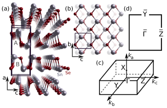
The crystal of SnSe consists of loosely bound layers that are, in the low temperature phase (T<800 K), built as an intricate knitting of tin and selenium atoms, in which each atom is linked to three of the other species by covalent bonds in trigonal pyramid geometry, forming distinct ridges along one of the crystal directions; see Figs. 1(a) and 1(b). The structure is such that a single layer, stretched into a flat sheet, would form a honeycomb lattice of alternating Sn and Se atoms. Neighboring layers are related by a center of inversion, but are lacking one themselves (DFT_Shi, ).
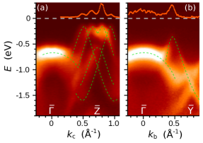
We start by describing the electronic band structure along two high-symmetry directions of the in-plane momentum space. The photoemission spectra recorded using =34 eV photons, displayed in Fig. 2, exhibit a multitude of downward dispersing bands at , from which several start rising in the direction of , and one in the direction of , reaching, however, somewhat lower final energy before turning down again. The overlaid curves explicate the full band configuration. This has been deduced from a set of photon energy-dependent measurements, having the third component of the crystal momentum span approximately one and a half bulk Brillouin zones (see Supplemental Material (Suppl, )).
When it comes to thermal and electronic transport properties of a material, they are in the valence band defined by the bands highest in energy, thus closest to the chemical potential. These will be discussed in more detail in what follows.
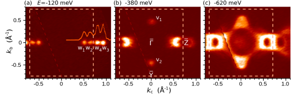
Figure 3 shows the momentum space configuration of the highest lying bands in the occupied band structure. At -120 meV four tiny collinear pockets, labeled start showing along – in the in-plane cut of the bulk Brillouin zone (Fig 3a). The map was acquired using 38 eV photons, representing the perpendicular momentum () shift of about 0.15 Å-1 with respect to the spectra in Fig. 2. No shift of the band maxima can be resolved either in momentum (they are found on either side, 0.08 and 0.22 Å-1 away from ) or energy (ARPES intensity starts appearing at -120 meV). Only a change in relative intensities is observed when the intensity profile in Fig. 3(a) is compared to the profile on top of Fig. 2(a), and is most likely due to a variation in optical transition probabilities. Were the maximum energies that the neighboring bands , reach different, their intensity profiles at constant energy would inevitably differ as well; that is not the case here. As the energy is lowered, the circular sections of these bands grow in size and soon merge. A gap of 250 meV opens up at marking the avoided crossing of the bands and . Interestingly, no such gaps are observed at the crossings of the other two pairs—, and , in Figs. 2(a), 3(b) or any of the figures in (Suppl, ).
Two other hole pockets, labeled , in Fig. 3(b), emerge in the perpendicular direction, centered at =±0.45 Å-1 with apices below some -380 meV. Lastly, the first photoemission signatures of the circular bands around become visible just below the energy of -600 meV.
Together with almost negligible dispersion of the bands across the material’s layers, that we observe in several other cuts using a range of photon energies and show in (Suppl, ), Fig. 3 adds to the notion of the unusual anisotropy of the band structure in all three crystal directions that can have significant consequences in many transport properties.
The effective mass and band velocity are the factors that decide the charge carrier mobility. In Fig. 4 we reexamine the two highest lying hole pockets and determine the effective mass by fitting the band dispersion to parabolas locally centered at pocket maxima.
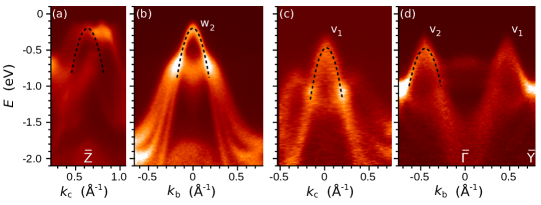
Four hole pockets in the vicinity of appear to have very similar initial dispersion along – direction, Fig. 4(a). Fitting to a parabola for any of the apices gives for the ’effective mass’ . The parabolic dispersion in the perpendicular direction (Fig. 4(b) is a cut for the second of the four) is slightly steeper, giving for the mass parameter of these pockets in the direction of the value of . The fitting curves place the top of the valence band at 200 meV below the chemical potential. The pockets along the – direction are best visible in ARPES when the excitation energy of 50 eV is used (this represents a shift of 0.57±0.03 Å-1 in , to be compared to of 0.54 Å-1). Their cuts in two perpendicular in-plane direction are shown in Figs. 4(c) and 4(d). Parabolic fitting places the centroid of the intensity at 480 meV below the chemical potential. The pockets have the effective mass of in the direction, and perpendicular to it. We show these summits and the fitting curves in greater detail in Fig. S3 of (Suppl, ).
The key to the efficient generation of the electric power and the record-high of 2.6 in high temperature phase of SnSe (T>800 K) is believed to be the unusually strong lattice anharmonicity and, consequently, a very low lattice thermal conductivity (ZhaoNAT, ; Carrete, ; Li, ). A similarly high of 2.0 was reported for p-doped single crystals in the low-temperature phase at 770 K. We will demonstrate here that the band structure of low-temperature SnSe has enough ingredients for a high thermopower, , and together with inherently low thermal conductivity of the crystal should support the efficient power generation or cooling, as assessed by maximizing the figure of merit . Unfortunately, the parameters in this equation available for such optimization—the electronic conductivity , the Seebeck coefficient , and the electronic thermal conductivity , are interdependent and mutually opposing.
In order to achieve a high Seebeck voltage, the band structure around the chemical potential needs to act as a filter that favors the heat diffusion by either cold carriers below the chemical potential or hot carriers above, and not both equally at the same time (Datta, ). That means having the chemical potential in the region of rapidly changing density of states, or better yet, in a semiconductor’s gap closer to one and farther from the other extremum of the conduction and valence bands. With the predicted band gap of around 800 meV, and the valence band maximum at 200 meV below the chemical potential, our SnSe samples appear naturally p-doped, and thus well suited for voltage generation. We note, however, that part of the asymmetry at low temperatures is likely coming from unequal onsets of density of states at two ends of the gap and may change as the chemical potential shifts at higher (DFT_Hong, ). The higher voltage, in general, will be generated by a temperature gradient the farther in (at 600K, =50 meV) the chemical potential is from the extremum of the conducting band (that is the valence band in p-doped, or the conduction band in n-doped crystals). This unfortunately leads to a small carrier density , reduced conductivity , and severely lowers the available thermopower.
Tin selenide, as we have seen above, has in the low-energy occupied band structure a few fast-dispersing bands capable of hosting highly mobile carriers. Coupled with structural faultlessness, their high mobility () can potentially balance out this reduced carrier density, providing enough conductivity for sizable thermopower.
Yet another feature works in favor of a high Seebeck coefficient in SnSe: the total band dispersion across the layers is extremely small. This implies a high effective mass . Assuming a tight-binding form of dispersion along , , where is below our detection limit of some 30-50 meV, we estimate to be or higher. When a thermal gradient is established along the layers, the uttermost value that the figure of merit can attain is expressed by the formula which summarizes the desired properties of an ideal thermoelectric material (Ref. (Sootsman, )):
The value is, fortuitously, proportional to . When conduction along either or high-symmetry directions is assumed (the above stands for or), the effective masses , we determined to be of comparable size for a number of valence bands, will in the above formula nearly cancel. Given the high anisotropy of the band structure, it should not be excluded that the ratio of the masses will increase when the two perpendicular in-plane directions are allowed to stray. The extreme in-plane band anisotropy of Fig. 3, not found in most but a few two-dimensional materials (Pletikosic, ), may be detrimental to the electronic heat transport as it limits the number of configurations available for the electrons to hop between in their random thermal motion. The anisotropy is also likely to affect the value of the scattering time of the carriers moving along the transport direction, and should be considered when optimizing the figure of merit as well. Interestingly enough, a recent angle-dependent conductivity study of SnSe finds the hole conductivity along almost four times higher than along (Xu, ). The quasiparticle effective masses on top of the valence band, which we find almost equal in both in-plane directions, cannot account for the observed anisotropy. Our toy-model calculation, by the recipe of Ref. (DFT_Gonzalez, ), for a single hole band having the dispersion of SnSe bands, indicates that the scattering times along the two directions should differ by an order of magnitude in order to reproduce the conductivity angular dependence (Suppl, ). This, curiously, does not lead to a notable Seebeck coefficient anisotropy and the power factor is only affected in the first order, through . Our model also nicely shows the benefits of having little out-of-plane dispersion: power factor maxima are achieved for completely filled bands in the direction, and increase as the bands narrow.
Finally, the ingredient in the band structure of SnSe that can easily lead to doubling the figure of merit is the band degeneracy factor , which reflects the number of available modes in thermoelectric transport. We have found four hole pockets along – that appear at exactly same energy in our constant energy maps, Fig. 3(a), and have the same initial parabolic dispersion. This is an important finding that ab initio thermoelectric transport simulations should rely on.
Density functional studies of bulk SnSe (DFT_Ding, ; DFT_Gomes, ; DFT_Gonzalez, ; DFT_Hong, ; DFT_Kutorasinski, ; DFT_Mori, ; DFT_Shafique, ; DFT_Shi, ; DFT_Sirikumara, ; DFT_Suzuki, ; DFT_Yu, ; DFT_Yang, ; DFT_RGuo, ) generally agree on the indirect nature of the band gap that forms between the valence band pockets along – and several electron pockets in the conduction band showing along –. The electron pocket minima themselves, however, happen to be only a few tens of meV apart. Most studies underestimate by some 200–300 meV the size of the gap that was experimentally determined to be 860 meV (ZhaoNAT, ). They also underestimate the difference in energy of the valence band pockets and , that we establish at 280 meV, the difference ranging from 0 meV in (DFT_Hong, ; DFT_Sirikumara, ) to 100–180 meV in (ZhaoSCI, ; DFT_Suzuki, ; DFT_Mori, ; DFT_Kutorasinski, ; DFT_Shi, ; DFT_Gomes, ; DFT_Gonzalez, ; DFT_Yang, ; DFT_RGuo, ). The discrepancy is likely to affect the existing predictions of transport properties at any higher temperatures. There is also a disagreement in the number and nature of the pockets along –: while majority of studies show four, the bands not always reach the same energy, and the 250 meV gap at due to the avoided crossing of the bands and never exists; most studies have it, however, between the pairs , and ,, where we, interestingly, observe none. Similar discrepancies exist for the effective masses, where calculations generally show much higher variability than we have observed. Ab initio simulations tend to ascribe the anisotropy of the transport properties to the difference in the effective masses, mostly disregarding the anisotropy of the scattering time (Xu, ). This all emphasizes the complexity of the band structure near band extrema and sensitivity of band structure calculations that we are hoping to steer in the right direction. Our results will also help modeling and exploration of ultrathin layers of SnSe in search for advantageous properties already found in black phosphorus—the band gap variable in size and (in)directionality (DFT_Guo, ; DFT_Kamal, ; DFT_Wang, ; DFT_Zhang, ), or enhancements of thermoelectric properties by band engineering and doping (Pei, ; DFT_Wang, ; ZhaoSCI, ; Duong, ; DFT_Shafique, ; Gharsallah, ; DFT_Zhu, ), spin dependent transport in a single layer (DFT_Shi, ), or valleytronics by selective optical pumping from the valence to the conduction band valleys using linearly polarized light (Rodin, ).
Acknowledgements.
This work was supported by the US Department of Energy, Contract No. DE-SC0012704, the ARO MURI program, Grant No. W911NF-12-1-0461, and was partly performed at the Nanoscience Foundry and Fine Analysis (NFFA-MIUR Italy, Progetti Internazionali) facility. The crystal growth at Princeton University was supported by the Gordon and Betty Moore Foundation, EPiQS initiative, grant GBMF-4412.References
- (1) L.-D. Zhao, S.-H. Lo, Y. Zhang, H. Sun, G. Tan, C. Uher, C. Wolverton, V. P. Dravid, M. G. Kanatzidis, Nature, 508, 373 (2014)
- (2) L.-D. Zhao, G. Tan, S. Hao, J. He, Y. Pei, H. Chi, H. Wang, S. Gong, H. Xu, V. P. Dravid, C. Uher, G. J. Snyder, C. Wolverton, M. G. Kanatzidis, Science, 351, 141 (2016)
- (3) M. A. Franzman, C. W. Schlenker, M. E. Thompson, R. L. Brutchey, J. Am. Chem. Soc., 132, 4060 (2010)
- (4) D.-H. Lee, C.-M. Park, ACS Appl. Mater. Interfaces, 9, 15439 (2017)
- (5) S. P. Koenig, R. A. Doganov, H. Schmidt, A. H. Castro Neto, B. Özyilmaz, Appl. Phys. Lett. 104, 103106 (2014)
- (6) F. Xia, H. Wang, Y. Jia, Nat. Commun., 5, 4458 (2014)
- (7) L. Li, Y. Yu, G. J. Ye, Q. Ge, X. Ou, H. Wu, D. Feng, X. H. Chen, Y. Zhang, Nat. Nanotechnol., 9, 372 (2014)
- (8) H. Liu, A. T. Neal, Z. Zhu, Z. Luo, X. Xu, D. Tománek, P. D. Ye, ACS Nano, 8, 4033 (2014)
- (9) M. Buscema, D. J. Groenendijk, S. I. Blanter, G. A. Steele, H. S. J. van der Zant, A. Castellanos-Gomez, Nano Lett., 14, 3347 (2014)
- (10) A. Carvalho, M. Wang, Xi Zhu, A. S. Rodin, H. Su, A. H. Castro Neto, Nat. Rev. Mater., 1, 16061 (2016)
- (11) J. Qiao, X. Kong, Z-X. Hu, F. Yang, W. Ji, Nat. Commun., 5, 4475 (2014)
- (12) G. Long, D. Maryenko, J. Shen, S. Xu, J. Hou, Z. Wu, W. K. Wong, T. Han, J. Lin, Y. Cai, R. Lortz, N. Wang, Nano Lett., 16, 7768 (2016)
- (13) Y. Huang, J. Qiao, K. He, S. Bliznakov, E. Sutter, X. Chen, D. Luo, F. Meng, D. Su, J. Decker, W. Ji, R. S. Ruoff, P. Sutter, Chem. Mater., 28, 8330 (2016)
- (14) M. M. Nassary, Turk. J. Phys. 33, 201–208 (2009)
- (15) H. Maier, D. R. Daniel, J. Electron. Mater., 6, 693 (1977)
- (16) L-C. Zhang, G. Qin, W-Z. Fang, H-J. Cui, Q-R. Zheng, Q-B. Yan, G. Su, Sci. Rep., 6, 19830 (2016)
- (17) L. Li, Z. Chen, Y. Hu, X. Wang, T. Zhang, W. Chen, Q. Wang, J. Am. Chem. Soc., 135, 1213 (2013)
- (18) H. Ju, J. Kim, ACS Nano, 10, 5730 (2016)
- (19) C. Zhang, H. Zin, M. Han, Z. Dai, H. Pang, Y. Zheng, Y-Q. Lan, J. Bao, J. Zhu, ACS Nano, 8, 3761 (2014)
- (20) X. Li, M.W. Lin, A. A. Puretzky, J. C. Idrobo, C. Ma, M. Chi, M. Yoon, C. M. Rouleau, I. Kravchenko, D. B. Geohegan, K. Xiao, Sci. Rep., 4, 5497 (2014)
- (21) A. J. Hong, L. Li, H. X. Zhu, Z. B. Yan, J. M. Liu, Z. F. Ren, J. Mater. Chem. A, 3, 13365 (2015)
- (22) H. I. Sirikumara, T. Jayasekera, arXiv:1703.05017v1
- (23) L. C. Gomes, A. Carvalho, Phys. Rev. B, 92, 085406 (2015)
- (24) R. L. González-Romero, A. Antonelli, J. J. Meléndez, arXiv:1612.05967v1
- (25) K. Kutorasinski, B. Wiendlocha, S. Kaprzyk, J. Tobola, Phys. Rev. B, 91, 205201 (2015)
- (26) H. Mori, H. Usui, M. Ochi, K. Kuroki, Phys. Rev. B 96, 085113 (2017)
- (27) G. Shi, E. Kioupakis, Nano Lett., 15, 6926 (2015); G. Shi, E. Kioupakis, J. Appl. Phys., 117, 065103 (2015)
- (28) Y. Suzuki, H. Nakamura, Phys. Chem. Chem. Phys., 17, 29647 (2015)
- (29) J. Yang, G. Zhang, G. Yang, C. Wang, Y. X. Wang, J. Alloys Compd.,644, 615 (2015)
- (30) R. Guo, X. Wang, Y. Kuang, B. Huang, Phys. Rev. B 92, 115202 (2015)
- (31) H. Yu, S. Dai, Y. Chen, Sci. Rep., 6, 26193 (2016)
- (32) G. Ding, G. Gao, K. Yao, Sci. Rep., 5, 9567 (2015)
- (33) A. Shafique, Y.-H. Shin, Sci. Rep., 7, 506 (2017)
- (34) See Supplemental Material at
- (35) J. Carrete, N. Mingo, S. Curtarolo, Appl. Phys. Lett., 105, 101907 (2014)
- (36) C. W. Li, J. Hong, A. F. May, D. Bansal, S. Chi, T. Hong, G. Ehlers,O. Delaire, Nature Phys, 11, 1063 (2015)
- (37) S. Datta, M. Lundstrom, A. Shakouri, nanoHUB.org, Thermoelectricity: From Atoms to Systems
- (38) J. R. Sootsman, D. Y. Chung, M. G. Kanatzidis, Angew. Chem. Int. Ed, 48, 8616 (2009)
- (39) I. Pletikosić, M. N. Ali, A. V. Fedorov, R. J. Cava, T. Valla, Phys. Rev. Lett. 113, 216601 (2014)
- (40) X. Xu, Q. Song, H. Wang, P. Li, K. Zhang, Y. Wang, K. Yuan, Z. Zang, Y. Ye, L. Dai, ACS Appl. Mater. Interfaces, 9, 12601 (2017)
- (41) S.-D. Guo, Y.-H. Wang, J. Appl. Phys., 121, 034302 (2017)
- (42) C. Kamal, A. Chakrabarti, M. Ezawa, Phys. Rev. B, 93, 125428 (2016)
- (43) F. Q. Wang, S. Zhang, J. Yu, Q. Wang, Nanoscale, 7, 15962 (2015)
- (44) H. Zhu, W. Sun, R. Armiento, P. Lazic, G. Ceder, Appl. Phys. Lett. 104, 082107 (2014)
- (45) A. T. Duong, V. Q. Nguyen, G. Duvjir, V. T. Duong, S. Kwon, J. Y. Song, J. K. Lee, J. E. Lee, S. Park, T. Min, J. Lee, J. Kim, S. Cho, Nat. Commun. 7, 13713 (2016)
- (46) M. Gharsallah, F. Serrano-Sánchez, N. M. Nemes, F. J. Mompeán, J. L. Martínez, M. T. Fernández-Díaz, F. Elhalouani, J. A. Alonso, Sci Rep. 6, 26774 (2016)
- (47) Y. Pei, H. Wang, G. J. Snyder, Adv. Mater. 24, 6125 (2012)
- (48) A. S. Rodin, Lidia C. Gomes, A. Carvalho, and A. H. Castro Neto, Phys. Rev. B, 93, 045431 (2016)
Band structure of a IV-VI black phosphorus analogue, the thermoelectric SnSe
I. Pletikosić
F. von Rohr
P. Pervan
P. K. Das
I. Vobornik
R. J. Cava
T. Valla
supplemental material
Figures S1 and S2 show the photon energy dependence of the ARPES maps of the band structure of SnSe. Due to the loss of information about the electron’s perpendicular momentum () upon leaving the surface, its value is estimated using the formula ( is the electron emission angle, 0 for with only one free parameter—the inner potential . The parameter measures the position of the bottom of the free-electron final band with respect to the vacuum level, and is usually found to be in the range from -10 to -20 eV. Both values for the inner potential that we used in Figures S1 and S2 confirm that the scans at six photon energies (30-50 eV) sampled along three half-widths () of the bulk Brillouin zone. The dispersion along of the highest-lying band has shown to be below our detection limit of 30–50 meV.
Figure S3 shows in a different aspect ratio and color scale band dispersion cuts of the pockets to along and cuts of pockets and in the perpendicular direction to justify the parabolic fitting of the bands on top of the valence band. In addition to the fits of the maxima of photoemission intensity, the latter two have been fitted by following half-width-at-half-maximum points from above as well.
The last section is describing our toy-model calculation of several transport properties for a single band resembling the bands forming the top of the valence band of SnSe. We argue that the slight mass anisotropy cannot be accounted for the factor of 4 difference in conductivities that has been observed along the and axes in SnSe.
![[Uncaptioned image]](/html/1707.04289/assets/x5.png)
Figure S1. Photon energy dependence of the ARPES maps of the band structure of SnSe. Perpendicular momentum and its relative change have been estimated using the inner potential of -12 eV. Dashed horizontal lines are shown at several characteristic energies as a guide to the eye.
![[Uncaptioned image]](/html/1707.04289/assets/x6.png)
Figure S2. Photon energy dependence of the ARPES maps of the band structure of SnSe. Perpendicular momentum and its relative change have been estimated using the inner potential of -16 eV. Dashed horizontal lines are shown at a few characteristic energies as a guide to the eye.
![[Uncaptioned image]](/html/1707.04289/assets/x7.png)
Figure S3. Several band dispersion cuts of the pockets and shown in a different aspect ratio exemplifying the parabolic shape of the bands. In addition to maximum-intensity parabolae (dashed lines) overlaid to the cuts BB of the pocket and CC of the pocket are parabolae following half-width-at-half-maximum points from above. These are free from any intensity coming from neighboring bands. Photons of 34, 30, and 50 eV were used, respectively.
A toy-model calculation of conductivity and Seebeck coefficient tensors , for a single band with the in-plane parabolic dispersion and a tight-binding-like dispersion across the layers, mimicking the valence band of SnSe:
in the Boltzmann transport equation formalism (González-Romero, arXiv:1612.05967)
and denote the Cartesian axes
![[Uncaptioned image]](/html/1707.04289/assets/x8.png)
assuming an elliptical angular dependence of the in-plane scattering time
Here, , , . Scattering time is usually taken to be of the order of several femtoseconds. The effective masses are nearly isotropic, , . meV.
Setting the ratio to 15, this simple model gives . The anisotropy found in angle-resolved transport measurements is as high as 4 (Xu et al, DOI:10.1021/acsami.7b00782).
Three values of , the total band dispersion across the layers, were used: meV, meV (lighter curves), and meV (darker curves).
Interestingly, the in-plane Seebeck coefficient tensor components are insensitive to the scattering time anisotropy, and the power factor is only affected in the first order, through .
Smaller band width in the perpendicular direction, i.e. weak bonding between the layers, leads to higher conductivities and power factors for a given chemical potential, but has negligible influence on the Seebeck coefficient.